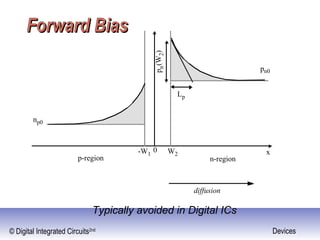
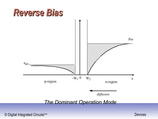
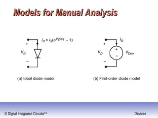
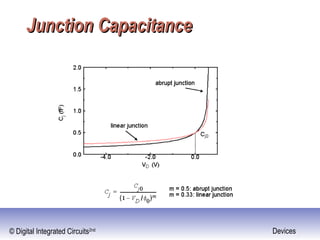
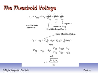
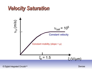
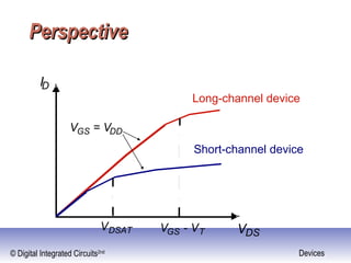
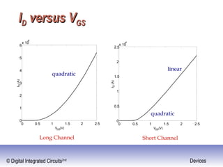
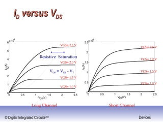
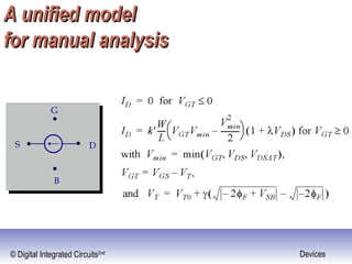
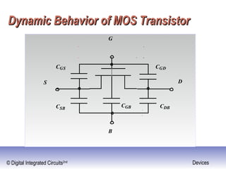
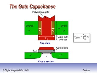
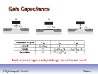
© Digital Integrated Circuits2nd Devices
Digital IntegratedDigital Integrated
CircuitsCircuits
A Design PerspectiveA Design Perspective
The DevicesThe Devices
Jan M. Rabaey
Anantha Chandrakasan
Borivoje Nikolic
July 30, 2002
© Digital Integrated Circuits2nd Devices
Goal of this chapterGoal of this chapter
 Present intuitive understanding of device
operation
 Introduction of basic device equations
 Introduction of models for manual
analysis
 Introduction of models for SPICE
simulation
 Analysis of secondary and deep-sub-
micron effects
 Future trends
© Digital Integrated Circuits2nd Devices
The DiodeThe Diode
n
p
p
n
B A
SiO2
Al
A
B
Al
A
B
Cross-section of pn-junction in an IC process
One-dimensional
representation diode symbol
Mostly occurring as parasitic element in Digital ICs
© Digital Integrated Circuits2nd Devices
Depletion RegionDepletion Region
hole diffusion
electron diffusion
p n
hole drift
electron drift
Charge
Density
Distance
x+
-
Electrical
xField
x
Potential
V
ξ
ρ
W2-W1
ψ0
(a) Current flow.
(b) Charge density.
(c) Electric field.
(d) Electrostatic
potential.
© Digital Integrated Circuits2nd Devices
Diode CurrentDiode Current
© Digital Integrated Circuits2nd Devices
Forward BiasForward Bias
x
pn0
np0
-W1 W2
0
pn(W2) n-regionp-region
Lp
diffusion
Typically avoided in Digital ICs
© Digital Integrated Circuits2nd Devices
Reverse BiasReverse Bias
x
pn0
np0
-W1 W20
n-regionp-region
diffusion
The Dominant Operation Mode
© Digital Integrated Circuits2nd Devices
Models for Manual AnalysisModels for Manual Analysis
VD
ID = IS(eVD/φT – 1)
+
–
VD
+
–
+
–
VDon
ID
(a) Ideal diode model (b) First-order diode model
© Digital Integrated Circuits2nd Devices
Junction CapacitanceJunction Capacitance
© Digital Integrated Circuits2nd Devices
Diffusion CapacitanceDiffusion Capacitance
© Digital Integrated Circuits2nd Devices
Secondary EffectsSecondary Effects
–25.0 –15.0 –5.0 5.0
VD (V)
–0.1
ID(A)
0.1
0
0
Avalanche Breakdown
© Digital Integrated Circuits2nd Devices
Diode ModelDiode Model
ID
RS
CD
+
-
VD
© Digital Integrated Circuits2nd Devices
SPICE ParametersSPICE Parameters
© Digital Integrated Circuits2nd Devices
What is a Transistor?What is a Transistor?
VGS ≥ VT
R o n
S D
A Switch!
|VGS|
An MOS Transistor
© Digital Integrated Circuits2nd Devices
The MOS TransistorThe MOS Transistor
Polysilicon Aluminum
© Digital Integrated Circuits2nd Devices
MOS Transistors -MOS Transistors -
Types and SymbolsTypes and Symbols
D
S
G
D
S
G
G
S
D D
S
G
NMOS Enhancement NMOS
PMOS
Depletion
Enhancement
B
NMOS with
Bulk Contact
© Digital Integrated Circuits2nd Devices
Threshold Voltage: ConceptThreshold Voltage: Concept
n+n+
p-substrate
DS
G
B
VGS
+
-
Depletion
Region
n-channel
© Digital Integrated Circuits2nd Devices
The Threshold VoltageThe Threshold Voltage
© Digital Integrated Circuits2nd Devices
The Body EffectThe Body Effect
-2.5 -2 -1.5 -1 -0.5 0
0.4
0.45
0.5
0.55
0.6
0.65
0.7
0.75
0.8
0.85
0.9
V
BS
(V)
V
T
(V)
© Digital Integrated Circuits2nd Devices
Current-Voltage RelationsCurrent-Voltage Relations
A good ol’ transistorA good ol’ transistor
Quadratic
Relationship
0 0.5 1 1.5 2 2.5
0
1
2
3
4
5
6
x 10
-4
VDS
(V)
ID
(A)
VGS= 2.5 V
VGS= 2.0 V
VGS= 1.5 V
VGS= 1.0 V
Resistive Saturation
VDS = VGS - VT
© Digital Integrated Circuits2nd Devices
Transistor in LinearTransistor in Linear
n+n+
p-substrate
D
S
G
B
VGS
xL
V(x)
+–
VDS
ID
MOS transistor and its bias conditions
© Digital Integrated Circuits2nd Devices
Transistor in SaturationTransistor in Saturation
n+n+
S
G
VGS
D
VDS > VGS - VT
VGS - VT
+-
Pinch-off
© Digital Integrated Circuits2nd Devices
Current-Voltage RelationsCurrent-Voltage Relations
Long-Channel DeviceLong-Channel Device
© Digital Integrated Circuits2nd Devices
A model for manual analysisA model for manual analysis
© Digital Integrated Circuits2nd Devices
Current-Voltage RelationsCurrent-Voltage Relations
The Deep-Submicron EraThe Deep-Submicron Era
Linear
Relationship
-4
VDS (V)
0 0.5 1 1.5 2 2.5
0
0.5
1
1.5
2
2.5
x 10
ID
(A)
VGS= 2.5 V
VGS= 2.0 V
VGS= 1.5 V
VGS= 1.0 V
Early Saturation
© Digital Integrated Circuits2nd Devices
Velocity SaturationVelocity Saturation
ξ (V/µm)ξc = 1.5
υn(m/s)
υsat = 105
Constant mobility (slope = µ)
Constant velocity
© Digital Integrated Circuits2nd Devices
PerspectivePerspective
ID
Long-channel device
Short-channel device
VDS
VDSAT VGS - VT
VGS = VDD
© Digital Integrated Circuits2nd Devices
IIDD versus Vversus VGSGS
0 0.5 1 1.5 2 2.5
0
1
2
3
4
5
6
x 10
-4
VGS(V)
ID(A)
0 0.5 1 1.5 2 2.5
0
0.5
1
1.5
2
2.5
x 10
-4
VGS(V)
ID(A)
quadratic
quadratic
linear
Long Channel Short Channel
© Digital Integrated Circuits2nd Devices
IIDD versus Vversus VDSDS
-4
VDS(V)
0 0.5 1 1.5 2 2.5
0
0.5
1
1.5
2
2.5
x 10
ID(A)
VGS= 2.5 V
VGS= 2.0 V
VGS= 1.5 V
VGS= 1.0 V
0 0.5 1 1.5 2 2.5
0
1
2
3
4
5
6
x 10
-4
VDS(V)
ID(A)
VGS= 2.5 V
VGS= 2.0 V
VGS= 1.5 V
VGS= 1.0 V
Resistive Saturation
VDS = VGS - VT
Long Channel Short Channel
© Digital Integrated Circuits2nd Devices
A unified modelA unified model
for manual analysisfor manual analysis
S D
G
B
© Digital Integrated Circuits2nd Devices
Simple Model versus SPICESimple Model versus SPICE
0 0.5 1 1.5 2 2.5
0
0.5
1
1.5
2
2.5
x 10
-4
VDS
(V)
ID
(A)
Velocity
Saturated
Linear
Saturated
VDSAT=VGT
VDS=VDSAT
VDS=VGT
© Digital Integrated Circuits2nd Devices
A PMOS TransistorA PMOS Transistor
-2.5 -2 -1.5 -1 -0.5 0
-1
-0.8
-0.6
-0.4
-0.2
0
x 10
-4
VDS (V)
ID(A)
Assume all variables
negative!
VGS = -1.0V
VGS = -1.5V
VGS = -2.0V
VGS = -2.5V
© Digital Integrated Circuits2nd Devices
Transistor ModelTransistor Model
for Manual Analysisfor Manual Analysis
© Digital Integrated Circuits2nd Devices
The Transistor as a SwitchThe Transistor as a Switch
VGS ≥ VT
R o n
S D
ID
VDS
VGS = VDD
VDD/2 VDD
R0
Rmid
ID
VDS
VGS = VDD
VDD/2 VDD
R0
Rmid
© Digital Integrated Circuits2nd Devices
The Transistor as a SwitchThe Transistor as a Switch
0.5 1 1.5 2 2.5
0
1
2
3
4
5
6
7
x 10
5
V
DD
(V)
R
eq
(Ohm)
© Digital Integrated Circuits2nd Devices
The Transistor as a SwitchThe Transistor as a Switch
© Digital Integrated Circuits2nd Devices
MOS CapacitancesMOS Capacitances
Dynamic BehaviorDynamic Behavior
© Digital Integrated Circuits2nd Devices
Dynamic Behavior of MOS TransistorDynamic Behavior of MOS Transistor
DS
G
B
CGDCGS
CSB CDBCGB
© Digital Integrated Circuits2nd Devices
The Gate CapacitanceThe Gate Capacitance
tox
n+ n+
Cross section
L
Gate oxide
xd xd
L d
Polysilicon gate
Top view
Gate-bulk
overlap
Source
n+
Drain
n+
W
© Digital Integrated Circuits2nd Devices
Gate CapacitanceGate Capacitance
S D
G
CGC
S D
G
CGC
S D
G
CGC
Cut-off Resistive Saturation
Most important regions in digital design: saturation and cut-off
© Digital Integrated Circuits2nd Devices
Gate CapacitanceGate Capacitance
WLCox
WLCox
2
2WLCox
3
CGC
CGCS
VDS /(VGS-VT
)
CGCD
0 1
CGC
CGCS = CGCD
CGC B
WLCox
WLCox
2
VGS
Capacitance as a function of VGS
(with VDS = 0)
Capacitance as a function of the
degree of saturation
© Digital Integrated Circuits2nd Devices
Measuring the Gate CapMeasuring the Gate Cap
2 1.52 1 2 0.5 0
3
4
5
6
7
8
9
10
3 102 16
2
VGS (V)
VGS
GateCapacitance(F)
0.5 1 1.5 22 2
I
© Digital Integrated Circuits2nd Devices
Diffusion CapacitanceDiffusion Capacitance
Bottom
Sidewall
Sidewall
Channel
Source
ND
Channel-stop implant
NA1
Substrate NA
W
xj
LS
© Digital Integrated Circuits2nd Devices
Junction CapacitanceJunction Capacitance
© Digital Integrated Circuits2nd Devices
Linearizing the Junction CapacitanceLinearizing the Junction Capacitance
Replace non-linear capacitance by
large-signal equivalent linear capacitance
which displaces equal charge
over voltage swing of interest
© Digital Integrated Circuits2nd Devices
Capacitances in 0.25Capacitances in 0.25 µµm CMOSm CMOS
processprocess
© Digital Integrated Circuits2nd Devices
The Sub-Micron MOS TransistorThe Sub-Micron MOS Transistor
 Threshold Variations
 Subthreshold Conduction
 Parasitic Resistances
© Digital Integrated Circuits2nd Devices
Threshold VariationsThreshold Variations
VT
L
Long-channel threshold Low VDS threshold
Threshold as a function of
the length (for low VDS)
Drain-induced barrier lowering
(for low L)
VDS
VT
© Digital Integrated Circuits2nd Devices
Sub-Threshold ConductionSub-Threshold Conduction
0 0.5 1 1.5 2 2.5
10
-12
10
-10
10
-8
10
-6
10
-4
10
-2
VGS
(V)
ID(A)
VT
Linear
Exponential
Quadratic
Typical values for S:
60 .. 100 mV/decade
The Slope Factor
ox
DnkT
qV
D
C
C
neII
GS
+=1,~ 0
S is ∆VGS for ID2/ID1 =10
© Digital Integrated Circuits2nd Devices
Sub-ThresholdSub-Threshold IIDD vsvs VVGSGS
VDS from 0 to 0.5V








−=
−
kT
qV
nkT
qV
D
DSGS
eeII 10
© Digital Integrated Circuits2nd Devices
Sub-ThresholdSub-Threshold IIDD vsvs VVDSDS
( )DS
kT
qV
nkT
qV
D VeeII
DSGS
⋅+







−=
−
λ110
VGS from 0 to 0.3V
© Digital Integrated Circuits2nd Devices
Summary of MOSFET OperatingSummary of MOSFET Operating
RegionsRegions
 Strong Inversion VGS >VT
 Linear (Resistive) VDS <VDSAT
 Saturated (Constant Current) VDS ≥VDSAT
 Weak Inversion (Sub-Threshold) VGS ≤VT
 Exponential in VGS with linear VDS dependence
© Digital Integrated Circuits2nd Devices
Parasitic ResistancesParasitic Resistances
W
LD
Drain
Drain
contact
Polysilicon gate
DS
G
RS RD
VGS,eff
© Digital Integrated Circuits2nd Devices
Latch-upLatch-up
© Digital Integrated Circuits2nd Devices
Future PerspectivesFuture Perspectives
25 nm FINFET MOS transistor

Chapter3

  • 1.
    © Digital IntegratedCircuits2nd Devices Digital IntegratedDigital Integrated CircuitsCircuits A Design PerspectiveA Design Perspective The DevicesThe Devices Jan M. Rabaey Anantha Chandrakasan Borivoje Nikolic July 30, 2002
  • 2.
    © Digital IntegratedCircuits2nd Devices Goal of this chapterGoal of this chapter  Present intuitive understanding of device operation  Introduction of basic device equations  Introduction of models for manual analysis  Introduction of models for SPICE simulation  Analysis of secondary and deep-sub- micron effects  Future trends
  • 3.
    © Digital IntegratedCircuits2nd Devices The DiodeThe Diode n p p n B A SiO2 Al A B Al A B Cross-section of pn-junction in an IC process One-dimensional representation diode symbol Mostly occurring as parasitic element in Digital ICs
  • 4.
    © Digital IntegratedCircuits2nd Devices Depletion RegionDepletion Region hole diffusion electron diffusion p n hole drift electron drift Charge Density Distance x+ - Electrical xField x Potential V ξ ρ W2-W1 ψ0 (a) Current flow. (b) Charge density. (c) Electric field. (d) Electrostatic potential.
  • 5.
    © Digital IntegratedCircuits2nd Devices Diode CurrentDiode Current
  • 6.
    © Digital IntegratedCircuits2nd Devices Forward BiasForward Bias x pn0 np0 -W1 W2 0 pn(W2) n-regionp-region Lp diffusion Typically avoided in Digital ICs
  • 7.
    © Digital IntegratedCircuits2nd Devices Reverse BiasReverse Bias x pn0 np0 -W1 W20 n-regionp-region diffusion The Dominant Operation Mode
  • 8.
    © Digital IntegratedCircuits2nd Devices Models for Manual AnalysisModels for Manual Analysis VD ID = IS(eVD/φT – 1) + – VD + – + – VDon ID (a) Ideal diode model (b) First-order diode model
  • 9.
    © Digital IntegratedCircuits2nd Devices Junction CapacitanceJunction Capacitance
  • 10.
    © Digital IntegratedCircuits2nd Devices Diffusion CapacitanceDiffusion Capacitance
  • 11.
    © Digital IntegratedCircuits2nd Devices Secondary EffectsSecondary Effects –25.0 –15.0 –5.0 5.0 VD (V) –0.1 ID(A) 0.1 0 0 Avalanche Breakdown
  • 12.
    © Digital IntegratedCircuits2nd Devices Diode ModelDiode Model ID RS CD + - VD
  • 13.
    © Digital IntegratedCircuits2nd Devices SPICE ParametersSPICE Parameters
  • 14.
    © Digital IntegratedCircuits2nd Devices What is a Transistor?What is a Transistor? VGS ≥ VT R o n S D A Switch! |VGS| An MOS Transistor
  • 15.
    © Digital IntegratedCircuits2nd Devices The MOS TransistorThe MOS Transistor Polysilicon Aluminum
  • 16.
    © Digital IntegratedCircuits2nd Devices MOS Transistors -MOS Transistors - Types and SymbolsTypes and Symbols D S G D S G G S D D S G NMOS Enhancement NMOS PMOS Depletion Enhancement B NMOS with Bulk Contact
  • 17.
    © Digital IntegratedCircuits2nd Devices Threshold Voltage: ConceptThreshold Voltage: Concept n+n+ p-substrate DS G B VGS + - Depletion Region n-channel
  • 18.
    © Digital IntegratedCircuits2nd Devices The Threshold VoltageThe Threshold Voltage
  • 19.
    © Digital IntegratedCircuits2nd Devices The Body EffectThe Body Effect -2.5 -2 -1.5 -1 -0.5 0 0.4 0.45 0.5 0.55 0.6 0.65 0.7 0.75 0.8 0.85 0.9 V BS (V) V T (V)
  • 20.
    © Digital IntegratedCircuits2nd Devices Current-Voltage RelationsCurrent-Voltage Relations A good ol’ transistorA good ol’ transistor Quadratic Relationship 0 0.5 1 1.5 2 2.5 0 1 2 3 4 5 6 x 10 -4 VDS (V) ID (A) VGS= 2.5 V VGS= 2.0 V VGS= 1.5 V VGS= 1.0 V Resistive Saturation VDS = VGS - VT
  • 21.
    © Digital IntegratedCircuits2nd Devices Transistor in LinearTransistor in Linear n+n+ p-substrate D S G B VGS xL V(x) +– VDS ID MOS transistor and its bias conditions
  • 22.
    © Digital IntegratedCircuits2nd Devices Transistor in SaturationTransistor in Saturation n+n+ S G VGS D VDS > VGS - VT VGS - VT +- Pinch-off
  • 23.
    © Digital IntegratedCircuits2nd Devices Current-Voltage RelationsCurrent-Voltage Relations Long-Channel DeviceLong-Channel Device
  • 24.
    © Digital IntegratedCircuits2nd Devices A model for manual analysisA model for manual analysis
  • 25.
    © Digital IntegratedCircuits2nd Devices Current-Voltage RelationsCurrent-Voltage Relations The Deep-Submicron EraThe Deep-Submicron Era Linear Relationship -4 VDS (V) 0 0.5 1 1.5 2 2.5 0 0.5 1 1.5 2 2.5 x 10 ID (A) VGS= 2.5 V VGS= 2.0 V VGS= 1.5 V VGS= 1.0 V Early Saturation
  • 26.
    © Digital IntegratedCircuits2nd Devices Velocity SaturationVelocity Saturation ξ (V/µm)ξc = 1.5 υn(m/s) υsat = 105 Constant mobility (slope = µ) Constant velocity
  • 27.
    © Digital IntegratedCircuits2nd Devices PerspectivePerspective ID Long-channel device Short-channel device VDS VDSAT VGS - VT VGS = VDD
  • 28.
    © Digital IntegratedCircuits2nd Devices IIDD versus Vversus VGSGS 0 0.5 1 1.5 2 2.5 0 1 2 3 4 5 6 x 10 -4 VGS(V) ID(A) 0 0.5 1 1.5 2 2.5 0 0.5 1 1.5 2 2.5 x 10 -4 VGS(V) ID(A) quadratic quadratic linear Long Channel Short Channel
  • 29.
    © Digital IntegratedCircuits2nd Devices IIDD versus Vversus VDSDS -4 VDS(V) 0 0.5 1 1.5 2 2.5 0 0.5 1 1.5 2 2.5 x 10 ID(A) VGS= 2.5 V VGS= 2.0 V VGS= 1.5 V VGS= 1.0 V 0 0.5 1 1.5 2 2.5 0 1 2 3 4 5 6 x 10 -4 VDS(V) ID(A) VGS= 2.5 V VGS= 2.0 V VGS= 1.5 V VGS= 1.0 V Resistive Saturation VDS = VGS - VT Long Channel Short Channel
  • 30.
    © Digital IntegratedCircuits2nd Devices A unified modelA unified model for manual analysisfor manual analysis S D G B
  • 31.
    © Digital IntegratedCircuits2nd Devices Simple Model versus SPICESimple Model versus SPICE 0 0.5 1 1.5 2 2.5 0 0.5 1 1.5 2 2.5 x 10 -4 VDS (V) ID (A) Velocity Saturated Linear Saturated VDSAT=VGT VDS=VDSAT VDS=VGT
  • 32.
    © Digital IntegratedCircuits2nd Devices A PMOS TransistorA PMOS Transistor -2.5 -2 -1.5 -1 -0.5 0 -1 -0.8 -0.6 -0.4 -0.2 0 x 10 -4 VDS (V) ID(A) Assume all variables negative! VGS = -1.0V VGS = -1.5V VGS = -2.0V VGS = -2.5V
  • 33.
    © Digital IntegratedCircuits2nd Devices Transistor ModelTransistor Model for Manual Analysisfor Manual Analysis
  • 34.
    © Digital IntegratedCircuits2nd Devices The Transistor as a SwitchThe Transistor as a Switch VGS ≥ VT R o n S D ID VDS VGS = VDD VDD/2 VDD R0 Rmid ID VDS VGS = VDD VDD/2 VDD R0 Rmid
  • 35.
    © Digital IntegratedCircuits2nd Devices The Transistor as a SwitchThe Transistor as a Switch 0.5 1 1.5 2 2.5 0 1 2 3 4 5 6 7 x 10 5 V DD (V) R eq (Ohm)
  • 36.
    © Digital IntegratedCircuits2nd Devices The Transistor as a SwitchThe Transistor as a Switch
  • 37.
    © Digital IntegratedCircuits2nd Devices MOS CapacitancesMOS Capacitances Dynamic BehaviorDynamic Behavior
  • 38.
    © Digital IntegratedCircuits2nd Devices Dynamic Behavior of MOS TransistorDynamic Behavior of MOS Transistor DS G B CGDCGS CSB CDBCGB
  • 39.
    © Digital IntegratedCircuits2nd Devices The Gate CapacitanceThe Gate Capacitance tox n+ n+ Cross section L Gate oxide xd xd L d Polysilicon gate Top view Gate-bulk overlap Source n+ Drain n+ W
  • 40.
    © Digital IntegratedCircuits2nd Devices Gate CapacitanceGate Capacitance S D G CGC S D G CGC S D G CGC Cut-off Resistive Saturation Most important regions in digital design: saturation and cut-off
  • 41.
    © Digital IntegratedCircuits2nd Devices Gate CapacitanceGate Capacitance WLCox WLCox 2 2WLCox 3 CGC CGCS VDS /(VGS-VT ) CGCD 0 1 CGC CGCS = CGCD CGC B WLCox WLCox 2 VGS Capacitance as a function of VGS (with VDS = 0) Capacitance as a function of the degree of saturation
  • 42.
    © Digital IntegratedCircuits2nd Devices Measuring the Gate CapMeasuring the Gate Cap 2 1.52 1 2 0.5 0 3 4 5 6 7 8 9 10 3 102 16 2 VGS (V) VGS GateCapacitance(F) 0.5 1 1.5 22 2 I
  • 43.
    © Digital IntegratedCircuits2nd Devices Diffusion CapacitanceDiffusion Capacitance Bottom Sidewall Sidewall Channel Source ND Channel-stop implant NA1 Substrate NA W xj LS
  • 44.
    © Digital IntegratedCircuits2nd Devices Junction CapacitanceJunction Capacitance
  • 45.
    © Digital IntegratedCircuits2nd Devices Linearizing the Junction CapacitanceLinearizing the Junction Capacitance Replace non-linear capacitance by large-signal equivalent linear capacitance which displaces equal charge over voltage swing of interest
  • 46.
    © Digital IntegratedCircuits2nd Devices Capacitances in 0.25Capacitances in 0.25 µµm CMOSm CMOS processprocess
  • 47.
    © Digital IntegratedCircuits2nd Devices The Sub-Micron MOS TransistorThe Sub-Micron MOS Transistor  Threshold Variations  Subthreshold Conduction  Parasitic Resistances
  • 48.
    © Digital IntegratedCircuits2nd Devices Threshold VariationsThreshold Variations VT L Long-channel threshold Low VDS threshold Threshold as a function of the length (for low VDS) Drain-induced barrier lowering (for low L) VDS VT
  • 49.
    © Digital IntegratedCircuits2nd Devices Sub-Threshold ConductionSub-Threshold Conduction 0 0.5 1 1.5 2 2.5 10 -12 10 -10 10 -8 10 -6 10 -4 10 -2 VGS (V) ID(A) VT Linear Exponential Quadratic Typical values for S: 60 .. 100 mV/decade The Slope Factor ox DnkT qV D C C neII GS +=1,~ 0 S is ∆VGS for ID2/ID1 =10
  • 50.
    © Digital IntegratedCircuits2nd Devices Sub-ThresholdSub-Threshold IIDD vsvs VVGSGS VDS from 0 to 0.5V         −= − kT qV nkT qV D DSGS eeII 10
  • 51.
    © Digital IntegratedCircuits2nd Devices Sub-ThresholdSub-Threshold IIDD vsvs VVDSDS ( )DS kT qV nkT qV D VeeII DSGS ⋅+        −= − λ110 VGS from 0 to 0.3V
  • 52.
    © Digital IntegratedCircuits2nd Devices Summary of MOSFET OperatingSummary of MOSFET Operating RegionsRegions  Strong Inversion VGS >VT  Linear (Resistive) VDS <VDSAT  Saturated (Constant Current) VDS ≥VDSAT  Weak Inversion (Sub-Threshold) VGS ≤VT  Exponential in VGS with linear VDS dependence
  • 53.
    © Digital IntegratedCircuits2nd Devices Parasitic ResistancesParasitic Resistances W LD Drain Drain contact Polysilicon gate DS G RS RD VGS,eff
  • 54.
    © Digital IntegratedCircuits2nd Devices Latch-upLatch-up
  • 55.
    © Digital IntegratedCircuits2nd Devices Future PerspectivesFuture Perspectives 25 nm FINFET MOS transistor