Downloaded 39 times


![Rohit Mongre Int. Journal of Engineering Research and Applications www.ijera.com
ISSN : 2248-9622, Vol. 4, Issue 8( Version 1), August 2014, pp. 146-153
www.ijera.com 153 | P a g e
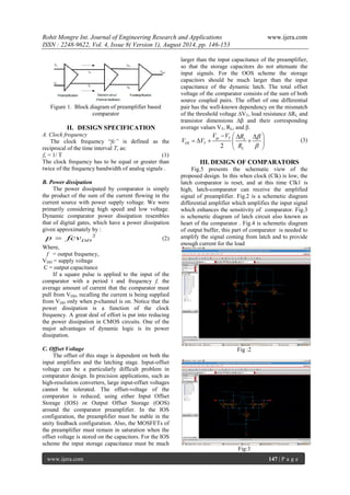
TABLE 2: SIMULATED RESULTS OF COMPARATOR.
TYPE OF COMPARATOR
Vir ps/ns
Vif Ps/ns
Vor Ps/ns
Vof Ps/ns
DELAY
SPEED= 1/DELAY Ghz
DESIGN I
2.7777ns
27.222ns
3.6864ns
28.7801ns
1.2333 ns
0.8108
DESIGN II
2.7777ns
27.222 ns
4.0752 ns
29.8079 ns
1.9416 ns
0.515
DESIGN III
55.5555 ps
20.1444 ns
164.496 ps
22.0799 ns
1.0222 ns
0.9782
DESIGN IV
55.5555 ps
20.1444 ns
156.277 ps
22.2280 ns
1.1171 ns
0.8951
V. CONCLUSION
In this paper simulation have been done in cadence virtuoso with 0.18μm UMC Technology. Finally simulation results of the comparators are shown in Table1 and Table2. As per the requirement of high speed and low power dissipation, DesignI i.e preamplifier based comparator having power dissipation of 108.0318μW , speed 0.8108 Ghz and delay of 1.2333ns confirms the expected circuit performance.
VI. ACKNOLEGEMENT
This work has been carried out in SMDP VLSI laboratory of the Electronics and Instrumentation Engineering Department of Shri G S Institute of Technology and Science, Indore, India. This SMDP VLSI project is funded by Ministry of Information and Communication Technology, Government of India. Authors are thankful to the Ministry for facilities provided under this project. REFERENCE [1] Wan Rosmaria Wan Ahmad, *Siti Lailatul Mohd Hassan, *Ili Shairah Abdul Halim, *Noor Ezan Abdullah *Ifzuan Mazlan “High Speed with Low Power Folding andInterpolating ADC Using Two Types of Comparator in CMOS 0.18um Technology” 2012 IEEE Symposium on Humanities, Science and Engineering Research [2] P. E. Allen, Douglas R. Holberg, “CMOS Analog Circuit Design”, Second Edition, Oxford University. [3] B. Razavi and B. A. Wooly, “Design Techniques for High-Speed, High Resolution Comparators”, IEEE Journal of Solid-State Circuit”, Vol. 27, No. 12, pp. 1916-1926, 1992 [4] Raja Mohd. Noor Hafizi Raja Daud, Mamun Bin Ibne Reaz, and Labonnah Farzana Rahman“Design and Analysis of Low Power and High Speed Dynamic Latch Comparator in 0.18 μm CMOS Process” International Journal of Information and Electronics Engineering, Vol. 2, No. 6, November 2012 [5] Eri Prasetyo*, Dominique Ginhac** , Michel Paindavoine*” Design and Implementation a 8 bits Pipeline Analog to Digital Converter in the Technology 0.6 m CMOS Process.” Makalah ada di prosiding ISSM05 , Paris, 30th September – 1st October 2005 [6] Christian Jesus B. FA YOMI I, Gordon W. ROBERTS ' and Molianiad SA WAN “ A 1- V, 1 0-bit Rail-to-Rail Successive Approximation Analog-to-Digital Converter in Standard 0.18pm CMOS Technology” 0- 7803-6685-9/01/$10.0002001 EEE [7] Jorge R. Fernandes, Manuel M. Silva “ A VERY LOW-POWER CMOS PARALLEL A/D CONVERTERFOR EMBEDDED APPLICATIONS”0780-8251- X/04/$17.002004 IEEE [8] Paul M. Furth, Member, IEEE, Yen-Chun Tsen, Vishnu B. Kulkarni and Thilak K. Poriyani House Raju Klipsch School of Electrical and Computer Engineering New Mexico State University “On the Design of Low-Power CMOS Comparators with Programmable Hysteresis” 978-1-4244- 7773-9/10/$26.00 ©2010 IEEE [9] HeungJun Jeon, Yong-Bin Kim “A CMOS LOW-POWER LOW-OFFSET AND HIGH- SPEED FULLY DYNAMIC LATCHED COMPARATOR” 978-1-4244-6683- 2/10/$26.00 ©2010 IEEE [10] Deepak Parashar1and Dr.R. S. Gamad2 Design of a CMOS Comparator with 0.18μm Technology For ADC Application [11] Shubhara Yewale, Radheshyam Gamad “Design of Low Power and High Speed CMOS Comparator for A/D Converter Application “Wireless Engineering and Technology, 2012, 3, 90-95 http://dx.doi.org/10.4236/wet.2012.32015 Published Online April 2012 (http://www.SciRP.org/journal/wet)](https://image.slidesharecdn.com/v04801146153-140910231822-phpapp01/85/Design-of-Low-Power-High-Speed-Comparator-with-0-18-m-Technology-for-ADC-Application-8-320.jpg)

This paper discusses the design of a high-speed, low-power CMOS comparator for analog to digital converter (ADC) applications, fabricated in a 0.18μm technology with a power supply of 1.8V. The proposed comparator exhibits a speed of 0.8108 GHz and a low power dissipation of 108.0318μW, achieving enhanced performance over earlier designs. Simulation results, comparisons of various comparator designs, and the implications for future ADC technologies are presented, confirming the effectiveness of the proposed preamplifier-based comparator.


![Analysis and design_of_a_low-voltage_low-power[1]](https://cdn.slidesharecdn.com/ss_thumbnails/analysisanddesignofalow-voltagelow-power1-140802050345-phpapp02-thumbnail.jpg?width=640&height=640&fit=bounds)


