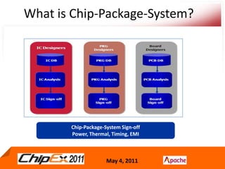
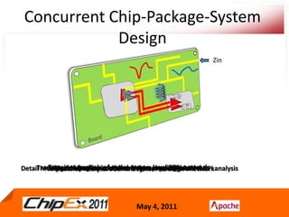
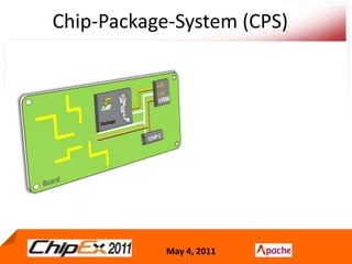
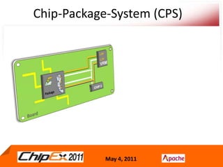
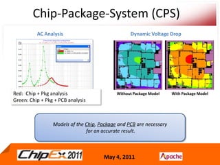
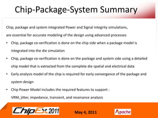
- Chip-Package-System (CPS) modeling involves integrated simulations of the chip, package and system to accurately model designs using advanced processes.
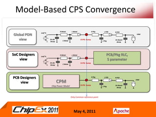
- CPS co-design verification requires chip and package co-verification from both the chip side using a package model and the package/system side using a detailed extracted chip model.
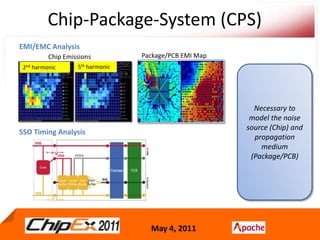
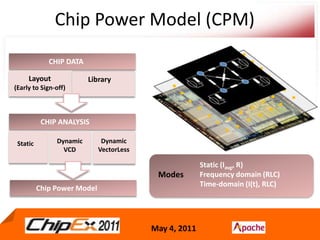
- Early analysis models of the chip are needed for early convergence of the package and system design.
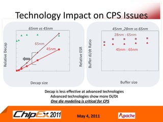
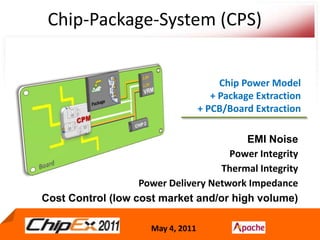
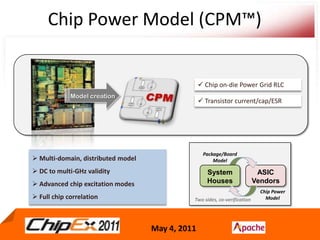
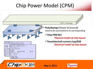
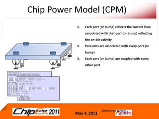
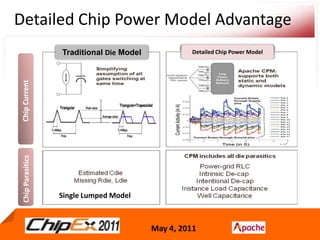
- A Chip Power Model extracted from the chip layout and data can be used to support simulations for issues like voltage regulation, jitter, impedance analysis, transients, and resonance effects across the CPS.