Download as PDF, PPTX


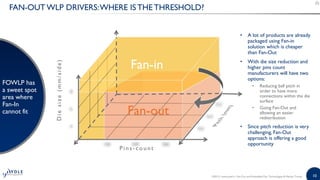


The document provides a comprehensive report on fan-out and embedded die technologies, detailing market trends, drivers, and forecasts for embedded wafer level packaging (WLP). It outlines the technological advancements, challenges, and supply chain dynamics within the semiconductor packaging industry. The analysis emphasizes the potential growth of fan-out WLP solutions in various applications, alongside the evolving role of embedded die packaging in the market.


