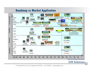
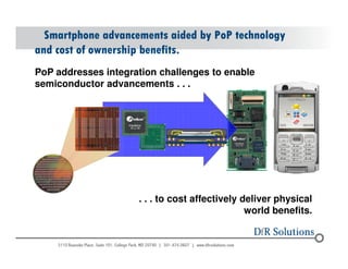
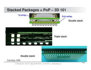
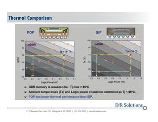
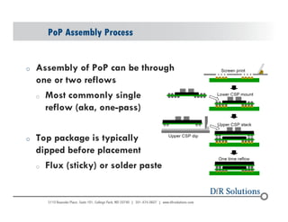
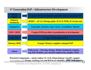
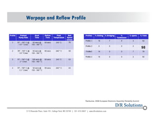
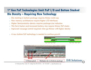
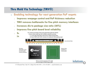
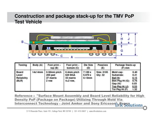
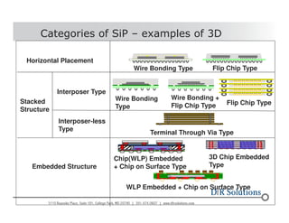
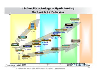
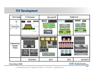
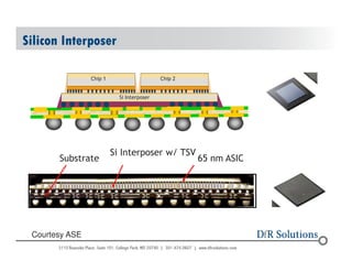
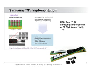
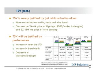
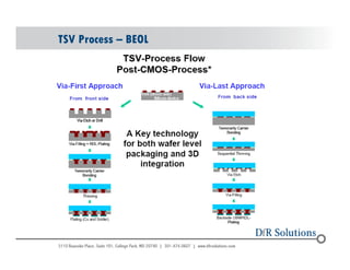
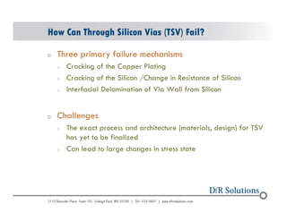
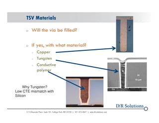
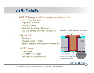
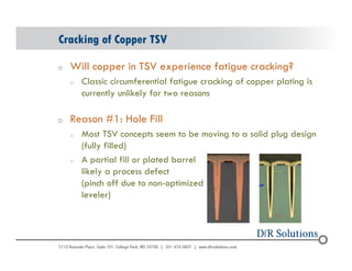
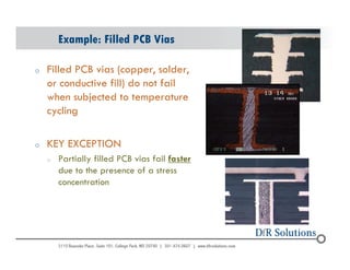
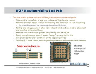
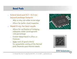
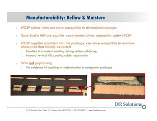
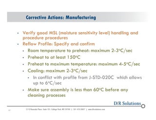
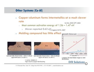
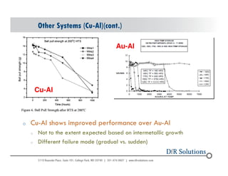
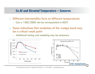
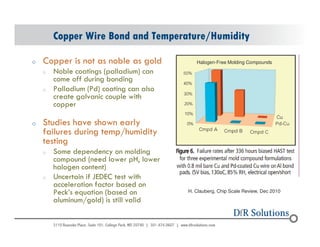
The Effect of Coating and Potting on the Reliability of QFN DevicesCheryl Tulkoff
The lack of a compliant lead structure makes QFN devices more susceptible to PCB warpage related failures:
oMechanical properties of the potting material
oGlass transition temperature (Tg)
oModulus should be specified above and below the Tg
oCTE should be specified above and below the Tg
The design of the housing:
oMay provide a surface to which the potting material can pull against when shrinking causing PCB warpage
oShould be designed to provide as close to a hydrostatic pressure as possible (equal pressure on all sides)
Package on-package interconnect for fan-out wafer level packagesInvensas
BVA® is a fine pitch vertical interconnect technology that forms package level 3D interconnects between active IC’s or passive devices, utilizing the existing wire bond infrastructure.
Intel Foveros and TSMC 3D SoIC are competing head-to-head for high-end packaging – How will Samsung react ?More information here : https://www.i-micronews.com/products/high-end-performance-packaging-3d-2-5d-integration-2020/
2.5D heterogeneous and 3D wafer-level stacking are reshaping the packaging landscape.
More information on that report at https://www.i-micronews.com/advanced-packaging-report/product/p2-5d-3d-tsv-wafer-level-stacking-technology-market-updates-2019.html
Qorvo QPF4006 39GHz GaN MMIC Front End Modulesystem_plus
The first MMIC FEM targeting 5G base stations and terminals using a 0.15µm GaN-on-SiC process.
More information on that report at: https://www.systemplus.fr/reverse-costing-reports/qorvo-qpf4006-39ghz-gan-mmic-front-end-module/
3DIC and 2.5D TSV Interconnect for Advanced Packaging: 2016 Business Update -...Yole Developpement
3D TSV technology is becoming a key solution platform for heterogeneous interconnection, high end memory and performance applications.
TSVs have been adopted for MEMS, Sensors, and Memory devices. What will the next technology driver be?
Through-silicon vias (TSVs) have now become the preferred interconnect choice for high-end memory. They are also an enabling technology for heterogeneous integration of logic circuits with CMOS image sensors (CIS), MEMS, sensors, and radio frequency (RF) filters. In the near future they will also enable photonics and LED function integration. The market for 3D TSV and 2.5D interconnect is expected to reach around two million wafers in 2020, expanding at a 22% compound annual growth rate (CAGR). The growth is driven by increased adoption of 3D memory devices in high-end graphics, high-performance computing, networking and data centers, and penetration into new areas, including fingerprint and ambient light sensors, RF filters and LEDs.
CIS still commanded more than 70% % share of TSV market wafer volume in 2015, although this will decrease to around 60% by 2020. This is primarily due to the growth of the other TSV applications, led by 3D memories, RF filters and fingerprint sensors (FPS). However, hybrid stacked technology, which uses direct copper-copper bonding, not TSVs, will penetrate around 30% of CIS production by 2020. The TSV markets for RF filters and FPS are expected to reach around $1.6B and $0.5B by 2020 respectively. The report will explain the market’s dynamics and give an overview of all segments and key markets. It will also provide market data in terms of revenues, units and wafer starts for all the different segments, including market share.
Temperature Cycling and Fatigue in ElectronicsCheryl Tulkoff
The majority of electronic failures occur due to thermally induced stresses and strains caused by excessive differences in coefficients of thermal expansion (CTE) across materials.
CTE mismatches occur in both 1st and 2nd level interconnects in electronics assemblies.
-1st level interconnects connect the die to a substrate.
-This substrate can be underfilled so there are both global and local CTE mismatches to consider.
-2nd level interconnects connect the substrate, or package, to the printed circuit board (PCB). This would be considered a “board level” CTE mismatch.
-Several stress and strain mitigation techniques exist including the use of conformal coating.
The purpose of this presentation is to show that accelerated testing can be successfully used to predict solder joint and plated through hole (PTH) fatigue behavior.
Hybrid bonding methods for lower temperature 3 d integration 1SUSS MicroTec
* Overview of primary 3D bonding processes
* Mechanics of metal bonding options
* Mechanics for hybrid bond materials
* Process requirement comparisons
* Equipment requirements for hybrid bond processes
Advanced Substrates Overview: From IC Package to Board - 2017 Report by Yole ...Yole Developpement
How can advanced substrates and boards bridge the gap created by front-end scaling?
Advanced substrates as a key enabler of future products and markets
In an uncertain, transformative semiconductor market, advanced packaging is one of the key technologies offering stability and a long-term solution. On one hand it can adapt to product diversification, offering more functionality, system integration, and performance, as well as potentially lower manufacturing cost; and on the other hand it can adhere to future scaling requirements. Advanced substrates are the key interconnect component of advanced packaging architectures and are critical in enabling future products and markets. For this reason, Yole has established this stand-alone dedicated advanced substrate activity, focused on exploring the market and technologies of PCBs, package substrates and RDLs. This first report will serve as an overview of advanced substrate technologies, markets, and supply chain, to be supported by subsequent in-depth reports.
Today’s advanced substrates in volume are Flip Chip (FC) substrates, 2.5D/3D TSV assemblies, and thin-film RDLs (Fan-Out WLP, or “FOWLP”) below an L/S resolution of 15/15 um and with transition below L/S < 10/10 um. These advanced substrates are traditionally linked to higher-end logic (CPUs/GPUs, DSPs, etc.) driven by ICs in the latest technology nodes in the computing, networking, mobile, and high-end consumer market segments (gaming, HD/Smart TV). However, due to additional form factor and low power demands, WLP and advanced FC substrates are also widespread in majority of smartphone functions: application processors, baseband, transceivers, filters, amplifiers, WiFi modules, drivers, codecs, power management, etc.
For more information, please visit our website: http://www.i-micronews.com/reports.html
Conformal Coating is applied to circuit cards to provide a dielectric layer on an electronic board. This layer functions as a membrane between the board and the environment. With this coating in place, the circuit card can withstand more moisture by increasing the surface resistance or surface insulation resistance (SIR). With a higher SIR board, the risk of problems such as cross talk, electrical leakage, intermittent signal losses, and shorting is reduced.
This reduction in moisture will also help to reduce metallic growth called dendrites and corrosion or oxidation. Conformal coating will also serve to shield a circuit card from dust, dirt and pollutants that can carry moisture and may be acidic or alkaline.
There are several types of conformal coating materials and the selection of one for your application must consider several variables. Silicones, polyurethanes, acrylics, epoxies and some of the newer hydrophilic materials offer many options to the user. However, the incorrect selection can result in huge problems with your CCA. For example, if you use silicone as your conformal coating material in a high sulfur environment, the silicone absorbs the sulfur and enhances the probability of silver migration on chip resistors and other forms of corrosion.
Thermo-Mechanical Simulation of Through Silicon Stack AssemblyKamal Karimanal
The electronics industry has been using Finite Element Analysis (FEA) to model IC package assembly process for understanding the effects of process conditions, material choice as well as design parameters. What was already practiced as an engineering-art within packaging organizations for monolithic IC packages has now become more complex due to the need for collaboration across organizational walls in the case of 3D stacking. The holistic solution needed for collaborative engineering of 3D stacking process calls for streamlined methodologies and information exchange protocols.
This presentation will introduce the idea of automated chip stacking process modeling approach with detailed discussions on inputs needed, gaps in existing modeling methodologies and output metrics of engineering relevance. The presentation will discuss wafer level warpage due to thinning and RDL films, their control, assembly implications of different under filling and encapsulation processes and pre attach warpage at reflow temperature
Today, plastic packaged integrated circuits are ubiquitous even for high-reliability applications. Reliability testing and standards play a key role in reliability engineering to achieve the necessary reliability performance. Traditional stress-based standards are easy to use but often over- or under-stress units and don’t focus on key vulnerabilities, particularly moisture-related ones. Knowledge-based standards have evolved to fix this, but rely on knowledge of mechanisms, control of board manufacturing conditions, and understanding and specifying end use conditions. This motivates a survey of plastic package mechanisms and testing with particular focus on moisture-related mechanisms and testing. The moisture-related examples will cover HAST testing, and the “popcorn” mechanism.
Learning Objectives
1.Understand the philosophy and methods behind reliability testing of ICs as applied to plastic-packaged ICs.
2.Learn the historical development of the JEDEC temperature-humidity-bias (HAST) moisture reliability testing standard.
3.Get a practical overview of key thermal, thermo-mechanical, moisture (chemical), and moisture (“popcorn”) mechanisms.
4.Appreciate how transformation of environmental conditions to conditions at the site of failure in the package is used to “scale” reliability models.
FR-4 PCBs for LED Applications: Testing Performance of PTH and Copper Pour In...Domestic PCB Fabrication
FR-4 Circuit Boards: Testing the performance of PTH and Copper Pour instead of Metal Core PCBs in LED Applications. From the June issue of SMT Magazine.
TSV Mining: Critical density in mining and changes to sustainable low cost pr...Totius Mining
TSV Mining's presentation on Critical Density in opencut mining operations and its impact on sustainable low cost production. From the mining boom, the increase in production for some operations may have crossed a point where sustainable low cost production may no longer be possible without redesign of how the operation functions.
This presentation talks about Breadth vs. Depth in the creative industry. It was a speaker aid for Tim McKenna of Azrael Group for Harrisburg BarCamp 6.
ANSYS RedHawk-CPA: New Paradigm for Faster Chip-Package ConvergenceAnsys
Due to the increasing size of SoCs and the variation in the switching current and parasitic profile across the chip, the individual connections between the SoC and the package at the C4 bump level need to be as granular as possible to provide resolution to the power analysis. To see the benefit from changes made to the chip and/or package in a timely manner requires that both layouts can be modified and modeled in an integrated manner. This presentation introduces RedHawk-CPA, a new feature which allows the inclusion of both chip and package layouts for a unified DC, transient and AC power integrity analysis. It will demonstrate how RedHawk-CPA can improve the level of accuracy as well as reduce the time to power closure. Learn more on our website: https://bit.ly/1ssSGM0
The quad flat pack no lead or quad flat non-leaded (QFN) is one of the fastest growing package types in the electronics industry today. While the advantages of QFNs are well documented, concerns arise with its reliability and manufacturability. Acceptance of this package, especially in long-life, severe-environment, high-reliability applications, is currently limited. One of the most common drivers for reliability failures is inappropriate adoption of new technologies, such as the case with QFN. In this presentation, we will review and discuss QFN related reliability concerns and challenges, and propose Physics-of-Failure (PoF) based approaches to allow the confident introduction of QFN components into electronics products.
A memory stack on logic 3D IC stack was considered for comparative study of warpage response to two different process choices, namely, Die to Die (D2D) and Package to Die (P2D) assembly. Process and reliability modeling software CielMech, and Commercial Finite Element Analysis (FEA) software ANSYS Mechanical were utilized to simulate thermo-mechanical effects of sequential chip attach, underfilling and encapsulation process steps for the chosen flows. Warpage at room temperature as well as attach temperature after each attach step were compared. Results indicated that underfill, substrate, and mold compound thermal strains play important roles in warpage evolution. Significant differences in the final assembled state warpage was predicted and is attributable to path dependence of warpage evolution.
First, the PCB board concept
PCB board is also known as the printed circuit board, is an important electronic component, is the support body of electronic components, is the provider of electrical connection of electronic components. As it is made using electronic printing, it is called a "printed" circuit board.
A printed circuit board(PCB) is a laminated sandwich structure of conductive and insulating layers.
There is a strong interest in understanding the surface mount
assembly requirements of QFN (Quad Flat No-Lead) type
packages due to their rapid industry acceptance.
For more details visit us at Solder.net
This paper provides guidelines in board design and surface mount of this package based on extensive surface mount experiments.
For more details at Solder.net
High Capacity Planar Supercapacitors and Lithium-Ion Batteries byModular Man...Bing Hsieh
High Capacity Planar Supercapacitors and Lithium Ion Batteries by Modular Manufacturing
Novel planar supercapacitors (SC) and lithium ion batteries (LIB) having interdigitated electrodes for large format applications will be presented. We will discuss the design principles of the new planar structures, their potential to give > 5X improvement in capacity over current supercapacitors, their pack designs, as well as low cost fabrication by modular manufacturing. The drawings given in the following link depict the plan view (top) and the cross-sectional view (bottom) of a planar LIB, wherein the dotted and the hatched areas are the positive and the negative electrodes respectively; the gray areas are the current collectors and the gray lines are the grid lines. Unlike the known interdigitated thin film microsupercapacitor design where the current collectors are situated on the top or bottom surfaces of the electrodes and paralleled to the plane of the substrate and can only exert limited weak fringe fields, the current collectors in our new design are running along the sidewalls of the electrodes and are perpendicular to the substrate and can thus provide strong direct fields, as indicated by the purple arrow, to promote facile ion movement across the entire thickness of the electrodes (20-100 µm). In addition, the relatively narrow inter-spaces between two opposite electrodes (20-100 µm) may allow much higher power densities than ever. Due to their scalability and low cost modular manufacturing processes by printing, the new planar SC/LIB may be designed for a wide range of applications such as mobile devices, transportation, and grid and distributed energy storage.
https://drive.google.com/file/d/0B7fDeNQTYRc9VDdOTTVYRmh2QWc/view?usp=sharing
Patented way to create Silicon Controlled Rectifiers in SOI technology Sofics
This paper introduces an SCR based ESD protection design for SOI technologies. It is explained how efficient SCR devices can be constructed in SOI. These devices outperform MOS devices by about 4 times.
Experimental data from 65nm and 130nm SOI is presented to support this.
What is CAF?
A growth consisting of a conductive copper-containing salt. It is created electrochemically and grows from the anode toward the cathode subsurface along the epoxy/glass interface.
Conductive Anodic Filament (CAF) formation does happen
o When it happens, it can cause a lot of pain
CAF behavior is relatively stable
o Limited change in key PCB technology (pitch, materials,
assembly)
CAF mitigation is well known (execute it!)
o Evaluate your designs
o Qualify your suppliers
Introducing higher dielectric constant (k > 10) insulators [mainly transition metal (TM) oxides] is therefore indispensable for the 70 nm technology node and beyond
TM silicates such as HfSiOx have been preferred because they have better thermal stability compared to their oxides. The dielectric constant of TM silicates is less than TM oxides but higher than silicon oxide.
COLLEGE BUS MANAGEMENT SYSTEM PROJECT REPORT.pdfKamal Acharya
The College Bus Management system is completely developed by Visual Basic .NET Version. The application is connect with most secured database language MS SQL Server. The application is develop by using best combination of front-end and back-end languages. The application is totally design like flat user interface. This flat user interface is more attractive user interface in 2017. The application is gives more important to the system functionality. The application is to manage the student’s details, driver’s details, bus details, bus route details, bus fees details and more. The application has only one unit for admin. The admin can manage the entire application. The admin can login into the application by using username and password of the admin. The application is develop for big and small colleges. It is more user friendly for non-computer person. Even they can easily learn how to manage the application within hours. The application is more secure by the admin. The system will give an effective output for the VB.Net and SQL Server given as input to the system. The compiled java program given as input to the system, after scanning the program will generate different reports. The application generates the report for users. The admin can view and download the report of the data. The application deliver the excel format reports. Because, excel formatted reports is very easy to understand the income and expense of the college bus. This application is mainly develop for windows operating system users. In 2017, 73% of people enterprises are using windows operating system. So the application will easily install for all the windows operating system users. The application-developed size is very low. The application consumes very low space in disk. Therefore, the user can allocate very minimum local disk space for this application.
Democratizing Fuzzing at Scale by Abhishek Aryaabh.arya
Presented at NUS: Fuzzing and Software Security Summer School 2024
This keynote talks about the democratization of fuzzing at scale, highlighting the collaboration between open source communities, academia, and industry to advance the field of fuzzing. It delves into the history of fuzzing, the development of scalable fuzzing platforms, and the empowerment of community-driven research. The talk will further discuss recent advancements leveraging AI/ML and offer insights into the future evolution of the fuzzing landscape.
Student information management system project report ii.pdfKamal Acharya
Our project explains about the student management. This project mainly explains the various actions related to student details. This project shows some ease in adding, editing and deleting the student details. It also provides a less time consuming process for viewing, adding, editing and deleting the marks of the students.
Cosmetic shop management system project report.pdfKamal Acharya
Buying new cosmetic products is difficult. It can even be scary for those who have sensitive skin and are prone to skin trouble. The information needed to alleviate this problem is on the back of each product, but it's thought to interpret those ingredient lists unless you have a background in chemistry.
Instead of buying and hoping for the best, we can use data science to help us predict which products may be good fits for us. It includes various function programs to do the above mentioned tasks.
Data file handling has been effectively used in the program.
The automated cosmetic shop management system should deal with the automation of general workflow and administration process of the shop. The main processes of the system focus on customer's request where the system is able to search the most appropriate products and deliver it to the customers. It should help the employees to quickly identify the list of cosmetic product that have reached the minimum quantity and also keep a track of expired date for each cosmetic product. It should help the employees to find the rack number in which the product is placed.It is also Faster and more efficient way.
Overview of the fundamental roles in Hydropower generation and the components involved in wider Electrical Engineering.
This paper presents the design and construction of hydroelectric dams from the hydrologist’s survey of the valley before construction, all aspects and involved disciplines, fluid dynamics, structural engineering, generation and mains frequency regulation to the very transmission of power through the network in the United Kingdom.
Author: Robbie Edward Sayers
Collaborators and co editors: Charlie Sims and Connor Healey.
(C) 2024 Robbie E. Sayers
Hybrid optimization of pumped hydro system and solar- Engr. Abdul-Azeez.pdffxintegritypublishin
Advancements in technology unveil a myriad of electrical and electronic breakthroughs geared towards efficiently harnessing limited resources to meet human energy demands. The optimization of hybrid solar PV panels and pumped hydro energy supply systems plays a pivotal role in utilizing natural resources effectively. This initiative not only benefits humanity but also fosters environmental sustainability. The study investigated the design optimization of these hybrid systems, focusing on understanding solar radiation patterns, identifying geographical influences on solar radiation, formulating a mathematical model for system optimization, and determining the optimal configuration of PV panels and pumped hydro storage. Through a comparative analysis approach and eight weeks of data collection, the study addressed key research questions related to solar radiation patterns and optimal system design. The findings highlighted regions with heightened solar radiation levels, showcasing substantial potential for power generation and emphasizing the system's efficiency. Optimizing system design significantly boosted power generation, promoted renewable energy utilization, and enhanced energy storage capacity. The study underscored the benefits of optimizing hybrid solar PV panels and pumped hydro energy supply systems for sustainable energy usage. Optimizing the design of solar PV panels and pumped hydro energy supply systems as examined across diverse climatic conditions in a developing country, not only enhances power generation but also improves the integration of renewable energy sources and boosts energy storage capacities, particularly beneficial for less economically prosperous regions. Additionally, the study provides valuable insights for advancing energy research in economically viable areas. Recommendations included conducting site-specific assessments, utilizing advanced modeling tools, implementing regular maintenance protocols, and enhancing communication among system components.
Industrial Training at Shahjalal Fertilizer Company Limited (SFCL)MdTanvirMahtab2
This presentation is about the working procedure of Shahjalal Fertilizer Company Limited (SFCL). A Govt. owned Company of Bangladesh Chemical Industries Corporation under Ministry of Industries.