www.altium.com
POWER DISTRIBUTION NETWORK IS NOT SO COMPLICATED
INTRODUCTION
When PCB designers hear the term “PDN”, or “Power Distribution Network”, it might conjure upnotions of bode plots, black
magic, and other mysterious, scary things. In reality, the goal of the PDN is as straightforward as are most of the PCB design
aspects that affect PDN performance. In this paper we’ll explain the various aspects of most PDN designs and how the PCB
designer can influence them.
OVERALL GOAL: SUFFICIENT CURRENT AND VOLTAGE TO ALL THE LOADS
The fundamental goal of a Power Distribution Network is very straightforward - provide enough current and voltage to every
load in order to meet their operation requirements. While the overall design of a PDN, including voltage regulators, on-
die decoupling, packaging, mounting of components, etc., is a very challenging science that requires specialized training and
experience, optimizing a PCB for PDN performance is less complicated since a PCB designer is limited in what they can do. In
this paper, we’ll focus on what to consider within the PCB layout to ensure that your PCB design will provide sufficient current
and voltage to all of your loads.
REQUIREMENT 1: SUFFICIENT METAL BETWEEN SOURCES AND LOADS
Ensuring there’s enough metal (usually copper) between each of the sources and their corresponding loads is the most critical
aspect of PDN design. On the bright side, for a nominal cost, IPC-2152 provides fairly straightforward guidelines on how to do
this. Given the maximum expected current and allowed temperature rise, the specification tells you what the minimum width
should be for your power shape. Unfortunately, a designer only using IPC-2152 will be over-designing their PCB while being
unaware of problems in their design, which comes with several limitations including:
Conservative Copper Pour
1. IPC-2152 width recommendations are very conservative.
They represent calculations using data from a thermal worst-case
scenario (2-layer board with no adjacent copper) and users typically
make the most conservative assumptions (e.g., minimum allowed
temperature rise). Designs made using only IPC-2152 may have
much larger power shapes than necessary.
2. IPC-2152 via recommendations are conservative.
This is especially problematic since vias for one power rail might
perforate the power shapes above and below, therefore via numbers
and sizes should be optimized. Designs made using only IPC-2152
may have larger or more power vias than necessary.
3. IPC-2152 only applies to the most straightforward design. A consistent width from source to load without any
perforations from vias or constrictions from components and other shapes. IPC-2152 doesn’t give guidance on how to
address imperfections in a design’s power shapes.
4. IPC-2152 gives no insight into placement of associated power rails. Voltage regulators often have specific require-
ments for the various power shapes associated with them, from input to output, possibly including feedback.
www.altium.com
POWER DISTRIBUTION NETWORK IS NOT SO COMPLICATED
Designers need better tools for optimizing the size and shape of their power (and ground) rails, commonly referred to as
“PI-DC” or “IR Drop”. Altium has integrated this capability into their design environment with PDN Analyzer to make it as easy
as possible to meet PDN requirements. Rather than relying on IPC-2152, a designer can analyze each power rail to see how
much metal is appropriate, including aspects that IPC-2152 doesn’t address such as:
— Distance between the source and loads
— Allowed voltage drop between the source and loads
— Allowed current through connector pins
— Compensating for perforations or constrictions in the ground plane from vias, connectors, etc.
— Parts of the power or ground shapes that carry no current, making them candidates for potential
issues such as EMI failures and excessive crosstalk
— Efficiency of power and ground shapes
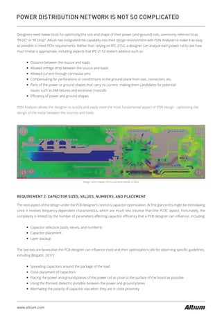
PDN Analyzer allows the designer to quickly and easily meet the most fundamental aspect of PDN design - optimizing the
design of the metal between the sources and loads.
Design with Copper Peninsula and Islands in Blue
REQUIREMENT 2: CAPACITOR SIZES, VALUES, NUMBERS, AND PLACEMENT
The next aspect of the design under the PCB designer’s control is capacitor optimization. At first glance this might be intimidating
since it involves frequency-dependent characteristics, which are much less intuitive than the PI-DC aspect. Fortunately, the
complexity is limited by the number of parameters affecting capacitor efficiency that a PCB designer can influence, including:
— Capacitor selection (sizes, values, and numbers)
— Capacitor placement
— Layer stackup
The last two are facets that the PCB designer can influence most and their optimization calls for observing specific guidelines,
including (Bogatin, 2011):
— Spreading capacitors around the package of the load
— Close placement of capacitors
— Placing the power and ground planes of the power rail as close to the surface of the board as possible
— Using the thinnest dielectric possible between the power and ground planes
— Alternating the polarity of capacitor vias when they are in close proximity
www.altium.com
POWER DISTRIBUTION NETWORK IS NOT SO COMPLICATED
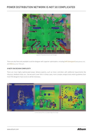
There are also free tools available to aid the designer with capacitor optimization, including Rolf Ostergaard (www.pdntool.com)
and Altera (as their “PDN tool”).
A NOTE ON DESIGN COMPLEXITY
There are more highly sophisticated power delivery systems, such as motor controllers with additional requirements like
inductors, feedback loops, etc., that we won’t cover here. In these cases, more complex analysis tools and/or guidelines than
most PCB designers have access to will be necessary.
Capacitor Placement Around Load Package
Current Density Plot on Complex Rigid-Flex Design
www.altium.com
POWER DISTRIBUTION NETWORK IS NOT SO COMPLICATED
THAT’S IT?
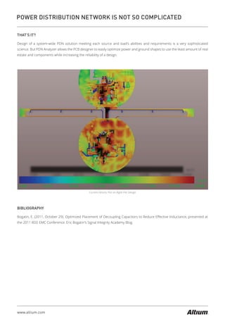
Design of a system-wide PDN solution meeting each source and load’s abilities and requirements is a very sophisticated
science. But PDN Analyzer allows the PCB designer to easily optimize power and ground shapes to use the least amount of real
estate and components while increasing the reliability of a design.
Current Density Plot on Rigid-Flex Design
BIBLIOGRAPHY
Bogatin, E. (2011, October 29). Optimized Placement of Decoupling Capacitors to Reduce Effective Inductance, presented at
the 2011 IEEE EMC Conference. Eric Bogatin's Signal Integrity Academy Blog.

Basics for pdn pcb designers

  • 2.
    www.altium.com POWER DISTRIBUTION NETWORKIS NOT SO COMPLICATED INTRODUCTION When PCB designers hear the term “PDN”, or “Power Distribution Network”, it might conjure upnotions of bode plots, black magic, and other mysterious, scary things. In reality, the goal of the PDN is as straightforward as are most of the PCB design aspects that affect PDN performance. In this paper we’ll explain the various aspects of most PDN designs and how the PCB designer can influence them. OVERALL GOAL: SUFFICIENT CURRENT AND VOLTAGE TO ALL THE LOADS The fundamental goal of a Power Distribution Network is very straightforward - provide enough current and voltage to every load in order to meet their operation requirements. While the overall design of a PDN, including voltage regulators, on- die decoupling, packaging, mounting of components, etc., is a very challenging science that requires specialized training and experience, optimizing a PCB for PDN performance is less complicated since a PCB designer is limited in what they can do. In this paper, we’ll focus on what to consider within the PCB layout to ensure that your PCB design will provide sufficient current and voltage to all of your loads. REQUIREMENT 1: SUFFICIENT METAL BETWEEN SOURCES AND LOADS Ensuring there’s enough metal (usually copper) between each of the sources and their corresponding loads is the most critical aspect of PDN design. On the bright side, for a nominal cost, IPC-2152 provides fairly straightforward guidelines on how to do this. Given the maximum expected current and allowed temperature rise, the specification tells you what the minimum width should be for your power shape. Unfortunately, a designer only using IPC-2152 will be over-designing their PCB while being unaware of problems in their design, which comes with several limitations including: Conservative Copper Pour 1. IPC-2152 width recommendations are very conservative. They represent calculations using data from a thermal worst-case scenario (2-layer board with no adjacent copper) and users typically make the most conservative assumptions (e.g., minimum allowed temperature rise). Designs made using only IPC-2152 may have much larger power shapes than necessary. 2. IPC-2152 via recommendations are conservative. This is especially problematic since vias for one power rail might perforate the power shapes above and below, therefore via numbers and sizes should be optimized. Designs made using only IPC-2152 may have larger or more power vias than necessary. 3. IPC-2152 only applies to the most straightforward design. A consistent width from source to load without any perforations from vias or constrictions from components and other shapes. IPC-2152 doesn’t give guidance on how to address imperfections in a design’s power shapes. 4. IPC-2152 gives no insight into placement of associated power rails. Voltage regulators often have specific require- ments for the various power shapes associated with them, from input to output, possibly including feedback.
  • 3.
    www.altium.com POWER DISTRIBUTION NETWORKIS NOT SO COMPLICATED Designers need better tools for optimizing the size and shape of their power (and ground) rails, commonly referred to as “PI-DC” or “IR Drop”. Altium has integrated this capability into their design environment with PDN Analyzer to make it as easy as possible to meet PDN requirements. Rather than relying on IPC-2152, a designer can analyze each power rail to see how much metal is appropriate, including aspects that IPC-2152 doesn’t address such as: — Distance between the source and loads — Allowed voltage drop between the source and loads — Allowed current through connector pins — Compensating for perforations or constrictions in the ground plane from vias, connectors, etc. — Parts of the power or ground shapes that carry no current, making them candidates for potential issues such as EMI failures and excessive crosstalk — Efficiency of power and ground shapes PDN Analyzer allows the designer to quickly and easily meet the most fundamental aspect of PDN design - optimizing the design of the metal between the sources and loads. Design with Copper Peninsula and Islands in Blue REQUIREMENT 2: CAPACITOR SIZES, VALUES, NUMBERS, AND PLACEMENT The next aspect of the design under the PCB designer’s control is capacitor optimization. At first glance this might be intimidating since it involves frequency-dependent characteristics, which are much less intuitive than the PI-DC aspect. Fortunately, the complexity is limited by the number of parameters affecting capacitor efficiency that a PCB designer can influence, including: — Capacitor selection (sizes, values, and numbers) — Capacitor placement — Layer stackup The last two are facets that the PCB designer can influence most and their optimization calls for observing specific guidelines, including (Bogatin, 2011): — Spreading capacitors around the package of the load — Close placement of capacitors — Placing the power and ground planes of the power rail as close to the surface of the board as possible — Using the thinnest dielectric possible between the power and ground planes — Alternating the polarity of capacitor vias when they are in close proximity
  • 4.
    www.altium.com POWER DISTRIBUTION NETWORKIS NOT SO COMPLICATED There are also free tools available to aid the designer with capacitor optimization, including Rolf Ostergaard (www.pdntool.com) and Altera (as their “PDN tool”). A NOTE ON DESIGN COMPLEXITY There are more highly sophisticated power delivery systems, such as motor controllers with additional requirements like inductors, feedback loops, etc., that we won’t cover here. In these cases, more complex analysis tools and/or guidelines than most PCB designers have access to will be necessary. Capacitor Placement Around Load Package Current Density Plot on Complex Rigid-Flex Design
  • 5.
    www.altium.com POWER DISTRIBUTION NETWORKIS NOT SO COMPLICATED THAT’S IT? Design of a system-wide PDN solution meeting each source and load’s abilities and requirements is a very sophisticated science. But PDN Analyzer allows the PCB designer to easily optimize power and ground shapes to use the least amount of real estate and components while increasing the reliability of a design. Current Density Plot on Rigid-Flex Design BIBLIOGRAPHY Bogatin, E. (2011, October 29). Optimized Placement of Decoupling Capacitors to Reduce Effective Inductance, presented at the 2011 IEEE EMC Conference. Eric Bogatin's Signal Integrity Academy Blog.