Download as PDF, PPTX


![Real Data on Single Crystals
0.00 5.00 10.00 15.00 20.00 25.00
Strain 2 ε (%)
0.00
5.00
10.00
15.00
20.00
Stressσ/2(N/mm2)
[100]
m=0.5
Polycrystal
[111]
33
15/9/11](https://image.slidesharecdn.com/wgc1manufacturingseptember2011-130809213311-phpapp01/85/Basics-of-Bonding-Wire-Manufacturing-33-320.jpg)


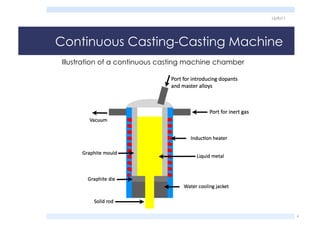
The document discusses the processing and material properties of gold and copper wire, detailing the manufacturing processes, chemical analysis, microstructure, and mechanical properties. It highlights the effect of dopants on the wire properties, the principles of continuous casting, and various analytical techniques for assessing metal purity. Additionally, it covers the plastic deformation during wire drawing, the influence of grain structure on mechanical behavior, and the final wire properties obtained through annealing.


