Download as PDF, PPTX


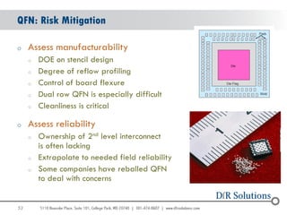


The document discusses the manufacturability and reliability challenges associated with Quad Flat No Leads (QFN) technology, highlighting issues related to solder wearout and testing parameters. It emphasizes the importance of understanding packaging processes and the influence of design on reliability, particularly in high-reliability applications. Additionally, the document outlines best practices for handling, inspection, and design considerations that can impact QFN manufacturing outcomes.


![Welcome To Smith 2011 English[1]](https://cdn.slidesharecdn.com/ss_thumbnails/welcometosmith2011english1-13080188251663-phpapp01-110613215148-phpapp01-thumbnail.jpg?width=640&height=640&fit=bounds)


![5G Explained! A High Level Overview [Introduction]](https://cdn.slidesharecdn.com/ss_thumbnails/5gexplainedahighleveloverview-260119165306-cc137a3e-thumbnail.jpg?width=640&height=640&fit=bounds)


