6/23/2014 © 2014 ANSYS, Inc. 1 
Sentinel-SSO: Full DDR-Bank 
Power and Signal Integrity 
Design Automation Conference 2014
6/23/2014 © 2014 ANSYS, Inc. 2 
Requirements for I/O DDR SSO Analysis 
Modeling 
– Package and board 
– I/O circuit and layout 
– PI + SI feedback 
Tool 
– Full bank capacity 
– Integrated modeling and 
simulation environment 
– Prototyping and what-if
6/23/2014 © 2014 ANSYS, Inc. 3 
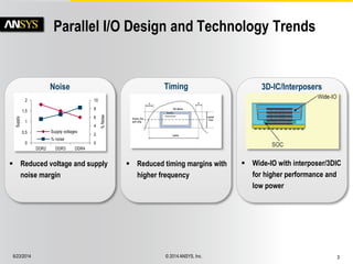
Parallel I/O Design and Technology Trends 
Noise 
 Reduced voltage and supply 
noise margin 
0 
2 
4 
6 
8 
10 
0 
0.5 
1 
1.5 
2 
DDR2 DDR3 DDR4 
% Noise 
Supply 
Supply voltages 
% noise 
Timing 
 Reduced timing margins with 
higher frequency 
3D-IC/Interposers 
 Wide-IO with interposer/3DIC 
for higher performance and 
low power
6/23/2014 © 2014 ANSYS, Inc. 4 
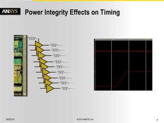
Power Integrity Effects on Timing
6/23/2014 © 2014 ANSYS, Inc. 5 
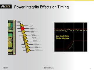
Power Integrity Effects on Timing 
Low Supply Noise 
Similar delay/slew
6/23/2014 © 2014 ANSYS, Inc. 6 
Power Integrity Effects on Timing 
Moderate Supply Noise 
Varying delay/slew
6/23/2014 © 2014 ANSYS, Inc. 7 
Power Integrity Effects on Timing 
High Supply Noise 
Increased Jitter Impact
6/23/2014 © 2014 ANSYS, Inc. 8 
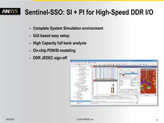
Sentinel-SSO: SI + PI for High-Speed DDR I/O 
– Complete System Simulation environment 
– GUI based easy setup 
– High Capacity full bank analysis 
– On-chip PDN/SI modeling 
– DDR JEDEC sign-off
6/23/2014 © 2014 ANSYS, Inc. 9 
Grid Weakness Reports 
Chip-Package-System 
SSO Analysis 
SSO Noise on 
Sensitive IP 
Chip-Signal-Model 
CSM 
JEDEC Signoff Reports 
Sentinel-SSO 
IC Data Channel Database 
3D PKG 
Extraction 
Multi-Simulator 
Support 
Chip IO 
Modeling 
Memory IO Model 
Chip Grid 
Modeling 
PI/SI Co-analysis Using Sentinel-SSO
6/23/2014 © 2014 ANSYS, Inc. 10 
Modeling Requirements for SSO Analysis 
– Accurate on-chip grid model 
– I/O models capturing impact of PDN noise 
– Accurate Power and Signal channel model 
– Accurate receiver models 
VRM Terminations 
I/O 
On-chip 
Grid 
Power 
Channel 
Signal 
Channel 
Chip Channel Receiver
6/23/2014 © 2014 ANSYS, Inc. 11 
Power Noise Impact on Signal Integrity 
Coupling in PKG/PCB reduced 
Modeling of Power Noise 
– On-chip PDN 
– Package Impedance 
– Accurate IO modeling 
Eye: with and without Power Noise 
With Power Noise 
Without Power Noise 
Source PG Bump 
Veff noise 
Strobe jitter DQ Jitter 
SNSSO 71mv 43.2ps 99.1ps 
Measured 73mv 42.0ps 92ps 
Accurate Measurement Correlation
6/23/2014 © 2014 ANSYS, Inc. 12 
Sentinel-SSO: I/O Buffer Modeling 
– CIOM: Non-linear device I/O buffer macro-model 
– Spice-level accuracy with full I/O bank capacity 
– Captures impact of P/G noise on signal 
– Load independent 
– Layout and circuit IP encryption
6/23/2014 © 2014 ANSYS, Inc. 13 
Full I/O Bank Capacity 
– 32bit and 64bit simulations common 
– Possible to simulate over 250 instances 
Size Run Time Simulation Time 
1 byte (all ciom) 25min 60ns 
1 byte (all xtor) 34hrs 39min 60ns 
4 bytes (all ciom) 2hrs 60ns 
IO Bank
6/23/2014 © 2014 ANSYS, Inc. 14 
Accurate On-die Modeling 
– Lumped models miss impedance and voltage variation across bank 
– Lumped models have less bandwidth 
– Reduced grid can model thousands of nodes 
Measurement correlated 
Cdie comparison 
Blue – CSM 
Green – meas. biased 
Red – meas. unbiased 
Lumped impedance 
(bottom yellow) 
Distributed impedance 
per instance 
Frequency 
Impedance
6/23/2014 © 2014 ANSYS, Inc. 15 
Signal/PG Coupling in Channel 
– DDR signal routing coupled to custom 
PG routing of PLL in package and board 
– PLL supply noise at metal1 level on chip 
determines circuit behavior 
DDR Bank 
I/O PG Supply PLL 
PLL PG Supply 
Coupling in PKG/PCB reduced 
Runtime reduced from 64hrs to 24min with CIOM 
“System Level PDN Analysis Enhancement Including 
I/O Subsystem Noise Modeling” DAC 2013
6/23/2014 © 2014 ANSYS, Inc. 16 
Accurately Capture Quiet Line Noise 
Noisy 
Quiet 
VSS has noise at chip 
Similar to VDD noise 
Signal supplied by 
PG voltage of driver 
2x Noise 
Asymmetric 
S-parameter pkg models 
cannot model reference-to-reference 
voltage differences! 
Symmetric 
RLCK package models allow for physical 
meaning to be assigned for voltage 
differences between all terminals
6/23/2014 © 2014 ANSYS, Inc. 17 
Sentinel-SSO Modeling Technologies 
Technology Impact Benefits 
Grid Modeling Accuracy 
 Captures on-die PDN noise 
 High bump resolution 
Chip IO Modeling Capacity 
 Efficient behavioral model 
 Captures power noise impact 
 High capacity simulation 
Channel Modeling Accuracy  True signal propagation 
DIE 
I/Os 
Package/Brd
6/23/2014 © 2014 ANSYS, Inc. 18 
Simulation & Reporting 
– Delay, Slew, Eye automatic measurements 
– JEDEC standard reporting 
– User configurable reports
6/23/2014 © 2014 ANSYS, Inc. 19 
Chip Aware System SI Using CSM 
• IP protected model of PHY 
• Model captures on-die PI/SI 
• Light weight behavioral model 
• Enables system level SI analysis 
v 
time 
Ω 
freq 
v 
time 
Power Nets 
Ground Nets 
Signal Nets
6/23/2014 © 2014 ANSYS, Inc. 20 
Summary 
• GUI based setup and simulation 
– Graphical connections and early analysis 
– Tcl commands to support batch mode operation 
• Accurate and efficient modeling 
– CSM, efficient IP neutral model of chip I/O bank 
– S-param conversion and SCB optimization 
• Reporting 
– Find and root cause die grid weaknesses 
– Waveforms, eye-diagrams, JEDEC 
Sentinel 
SSO 
JEDEC 
Reporting 
Prototyping 
Channel 
Optimization 
Model 
Generation

Full DDR Bank Power and Signal Integrity Analysis with Chip-Package-System Coupling

  • 1.
    6/23/2014 © 2014ANSYS, Inc. 1 Sentinel-SSO: Full DDR-Bank Power and Signal Integrity Design Automation Conference 2014
  • 2.
    6/23/2014 © 2014ANSYS, Inc. 2 Requirements for I/O DDR SSO Analysis Modeling – Package and board – I/O circuit and layout – PI + SI feedback Tool – Full bank capacity – Integrated modeling and simulation environment – Prototyping and what-if
  • 3.
    6/23/2014 © 2014ANSYS, Inc. 3 Parallel I/O Design and Technology Trends Noise  Reduced voltage and supply noise margin 0 2 4 6 8 10 0 0.5 1 1.5 2 DDR2 DDR3 DDR4 % Noise Supply Supply voltages % noise Timing  Reduced timing margins with higher frequency 3D-IC/Interposers  Wide-IO with interposer/3DIC for higher performance and low power
  • 4.
    6/23/2014 © 2014ANSYS, Inc. 4 Power Integrity Effects on Timing
  • 5.
    6/23/2014 © 2014ANSYS, Inc. 5 Power Integrity Effects on Timing Low Supply Noise Similar delay/slew
  • 6.
    6/23/2014 © 2014ANSYS, Inc. 6 Power Integrity Effects on Timing Moderate Supply Noise Varying delay/slew
  • 7.
    6/23/2014 © 2014ANSYS, Inc. 7 Power Integrity Effects on Timing High Supply Noise Increased Jitter Impact
  • 8.
    6/23/2014 © 2014ANSYS, Inc. 8 Sentinel-SSO: SI + PI for High-Speed DDR I/O – Complete System Simulation environment – GUI based easy setup – High Capacity full bank analysis – On-chip PDN/SI modeling – DDR JEDEC sign-off
  • 9.
    6/23/2014 © 2014ANSYS, Inc. 9 Grid Weakness Reports Chip-Package-System SSO Analysis SSO Noise on Sensitive IP Chip-Signal-Model CSM JEDEC Signoff Reports Sentinel-SSO IC Data Channel Database 3D PKG Extraction Multi-Simulator Support Chip IO Modeling Memory IO Model Chip Grid Modeling PI/SI Co-analysis Using Sentinel-SSO
  • 10.
    6/23/2014 © 2014ANSYS, Inc. 10 Modeling Requirements for SSO Analysis – Accurate on-chip grid model – I/O models capturing impact of PDN noise – Accurate Power and Signal channel model – Accurate receiver models VRM Terminations I/O On-chip Grid Power Channel Signal Channel Chip Channel Receiver
  • 11.
    6/23/2014 © 2014ANSYS, Inc. 11 Power Noise Impact on Signal Integrity Coupling in PKG/PCB reduced Modeling of Power Noise – On-chip PDN – Package Impedance – Accurate IO modeling Eye: with and without Power Noise With Power Noise Without Power Noise Source PG Bump Veff noise Strobe jitter DQ Jitter SNSSO 71mv 43.2ps 99.1ps Measured 73mv 42.0ps 92ps Accurate Measurement Correlation
  • 12.
    6/23/2014 © 2014ANSYS, Inc. 12 Sentinel-SSO: I/O Buffer Modeling – CIOM: Non-linear device I/O buffer macro-model – Spice-level accuracy with full I/O bank capacity – Captures impact of P/G noise on signal – Load independent – Layout and circuit IP encryption
  • 13.
    6/23/2014 © 2014ANSYS, Inc. 13 Full I/O Bank Capacity – 32bit and 64bit simulations common – Possible to simulate over 250 instances Size Run Time Simulation Time 1 byte (all ciom) 25min 60ns 1 byte (all xtor) 34hrs 39min 60ns 4 bytes (all ciom) 2hrs 60ns IO Bank
  • 14.
    6/23/2014 © 2014ANSYS, Inc. 14 Accurate On-die Modeling – Lumped models miss impedance and voltage variation across bank – Lumped models have less bandwidth – Reduced grid can model thousands of nodes Measurement correlated Cdie comparison Blue – CSM Green – meas. biased Red – meas. unbiased Lumped impedance (bottom yellow) Distributed impedance per instance Frequency Impedance
  • 15.
    6/23/2014 © 2014ANSYS, Inc. 15 Signal/PG Coupling in Channel – DDR signal routing coupled to custom PG routing of PLL in package and board – PLL supply noise at metal1 level on chip determines circuit behavior DDR Bank I/O PG Supply PLL PLL PG Supply Coupling in PKG/PCB reduced Runtime reduced from 64hrs to 24min with CIOM “System Level PDN Analysis Enhancement Including I/O Subsystem Noise Modeling” DAC 2013
  • 16.
    6/23/2014 © 2014ANSYS, Inc. 16 Accurately Capture Quiet Line Noise Noisy Quiet VSS has noise at chip Similar to VDD noise Signal supplied by PG voltage of driver 2x Noise Asymmetric S-parameter pkg models cannot model reference-to-reference voltage differences! Symmetric RLCK package models allow for physical meaning to be assigned for voltage differences between all terminals
  • 17.
    6/23/2014 © 2014ANSYS, Inc. 17 Sentinel-SSO Modeling Technologies Technology Impact Benefits Grid Modeling Accuracy  Captures on-die PDN noise  High bump resolution Chip IO Modeling Capacity  Efficient behavioral model  Captures power noise impact  High capacity simulation Channel Modeling Accuracy  True signal propagation DIE I/Os Package/Brd
  • 18.
    6/23/2014 © 2014ANSYS, Inc. 18 Simulation & Reporting – Delay, Slew, Eye automatic measurements – JEDEC standard reporting – User configurable reports
  • 19.
    6/23/2014 © 2014ANSYS, Inc. 19 Chip Aware System SI Using CSM • IP protected model of PHY • Model captures on-die PI/SI • Light weight behavioral model • Enables system level SI analysis v time Ω freq v time Power Nets Ground Nets Signal Nets
  • 20.
    6/23/2014 © 2014ANSYS, Inc. 20 Summary • GUI based setup and simulation – Graphical connections and early analysis – Tcl commands to support batch mode operation • Accurate and efficient modeling – CSM, efficient IP neutral model of chip I/O bank – S-param conversion and SCB optimization • Reporting – Find and root cause die grid weaknesses – Waveforms, eye-diagrams, JEDEC Sentinel SSO JEDEC Reporting Prototyping Channel Optimization Model Generation