Downloaded 373 times


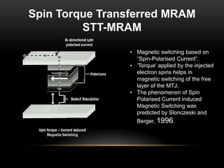
![• Resistance of the memory bit either low or high
depending on the relative magnetization,
[parallel or antiparallel] of the free layer with
respect to the fixed layer.
• Information storage a function of the magnetic
orientation of the ferromagnetic layers in the
MTJ.
• Therefore, external agent to switch the magnetic
orientation.
• Multiple ways in which the magnetic switching
can be done.](https://image.slidesharecdn.com/41me-131122143301-phpapp01/85/MRAM-Its-Applications-10-320.jpg)


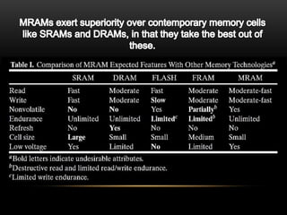
The document discusses the challenges posed by Moore's Law to integrated circuits, particularly concerning power dissipation and thermal noise, leading to a potential shift towards magneto-resistive RAM (MRAM) as a solution. MRAM offers advantages such as non-volatility and high-speed performance, with various types like STT-MRAM and FW-MRAM presented for mobile applications and logic computing. Additionally, it highlights recent research developments and potential industry applications of MRAM technology.


