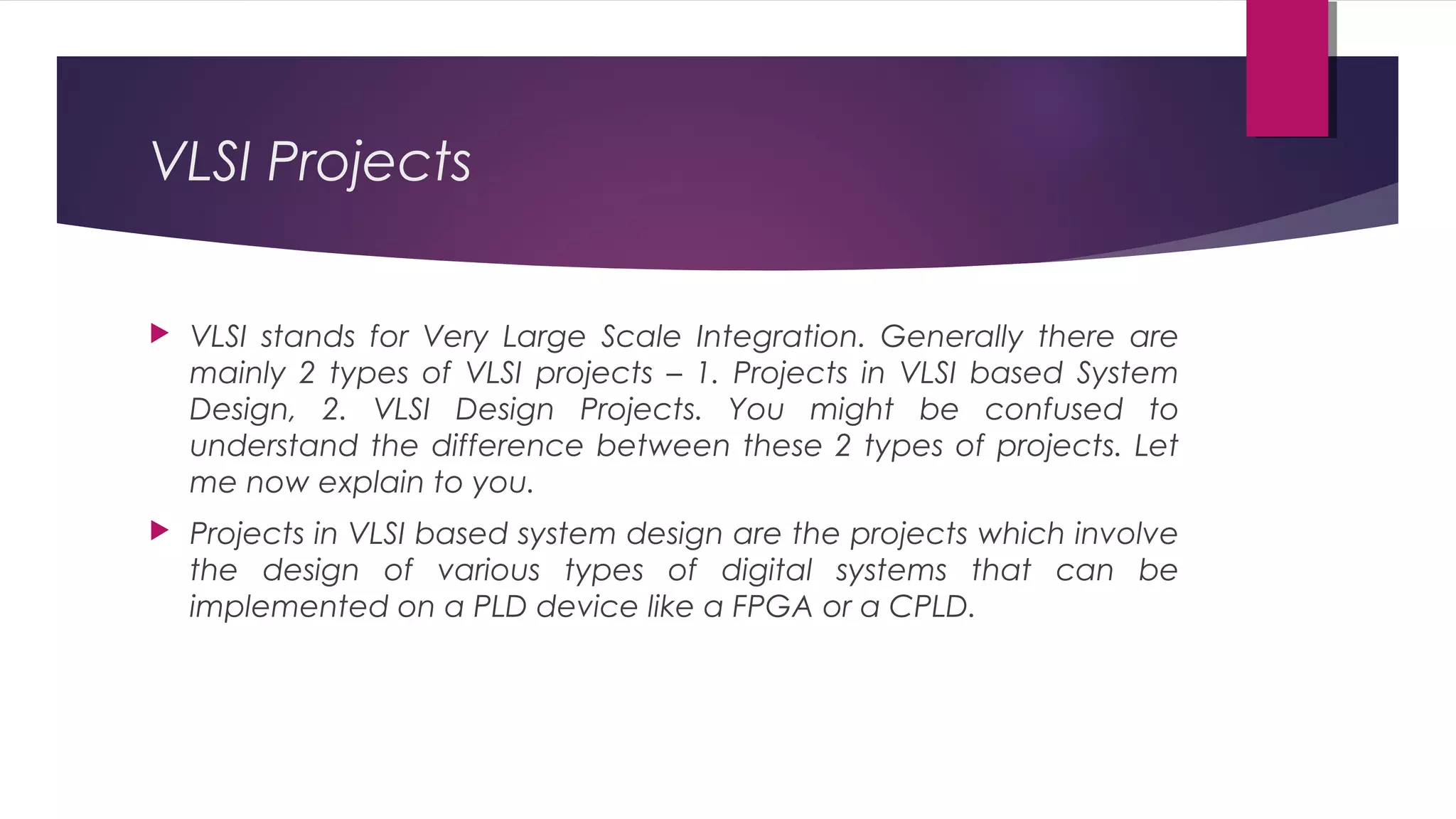
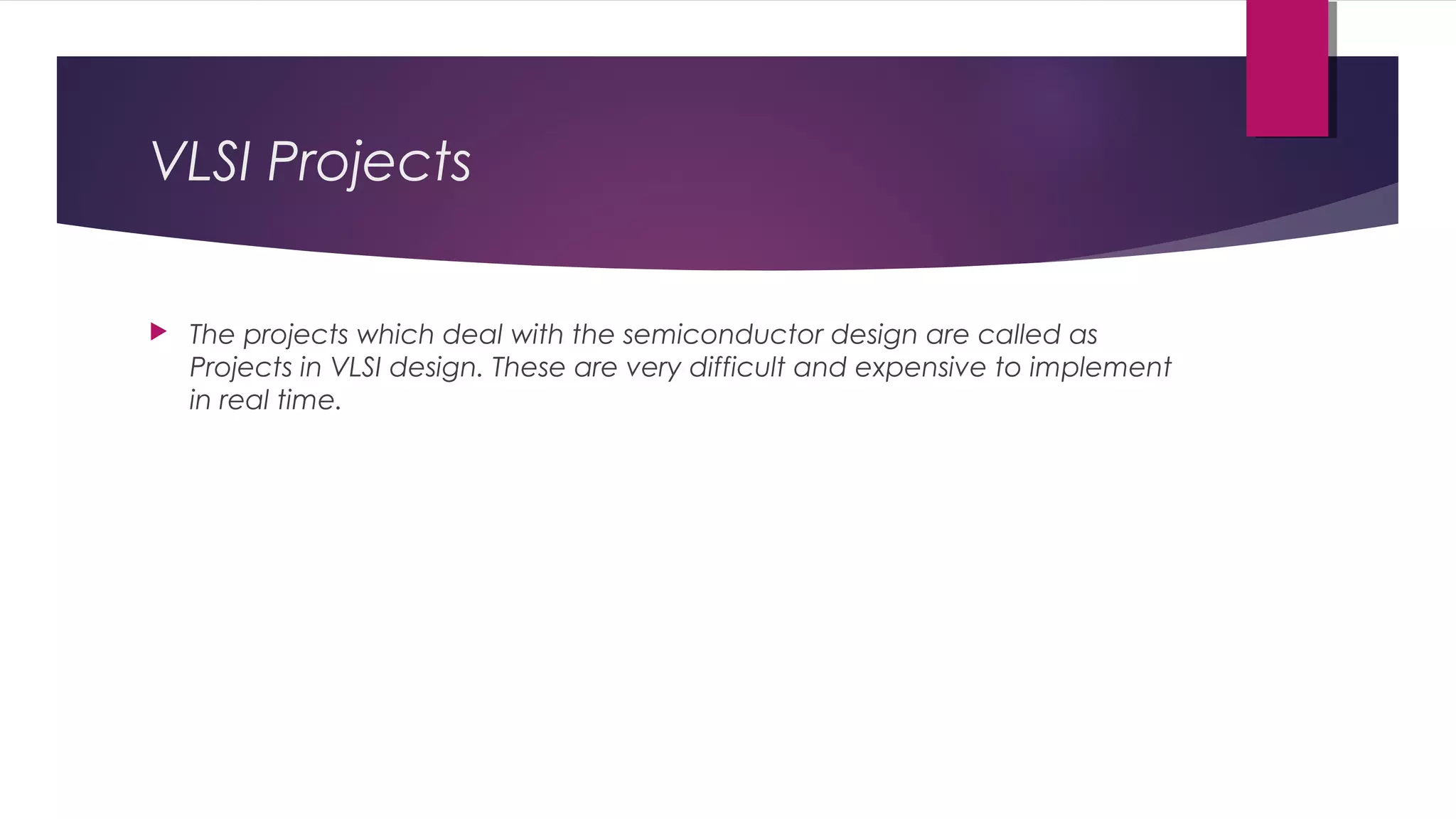
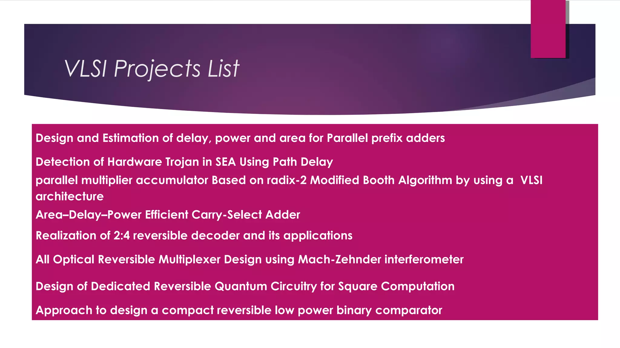
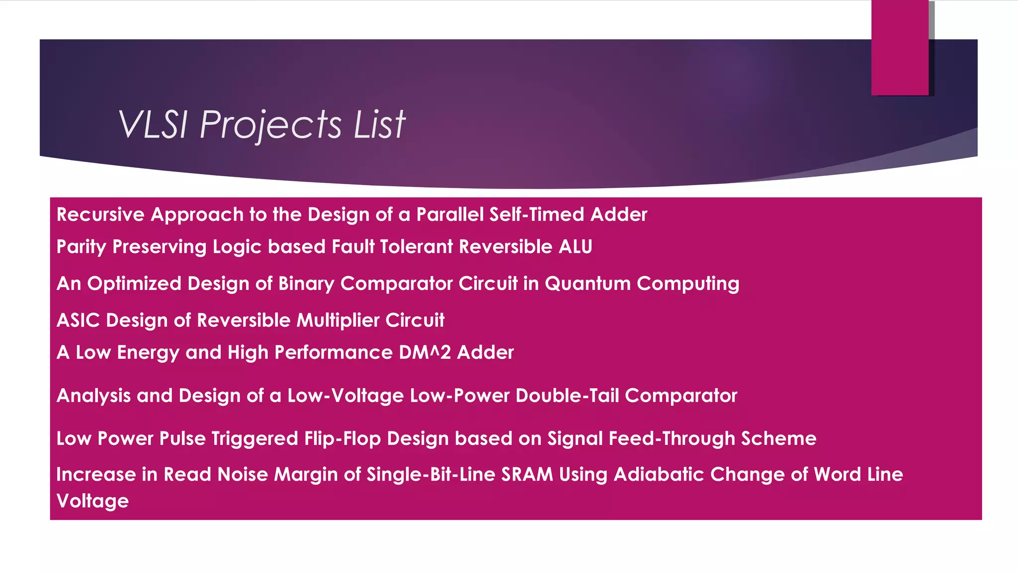
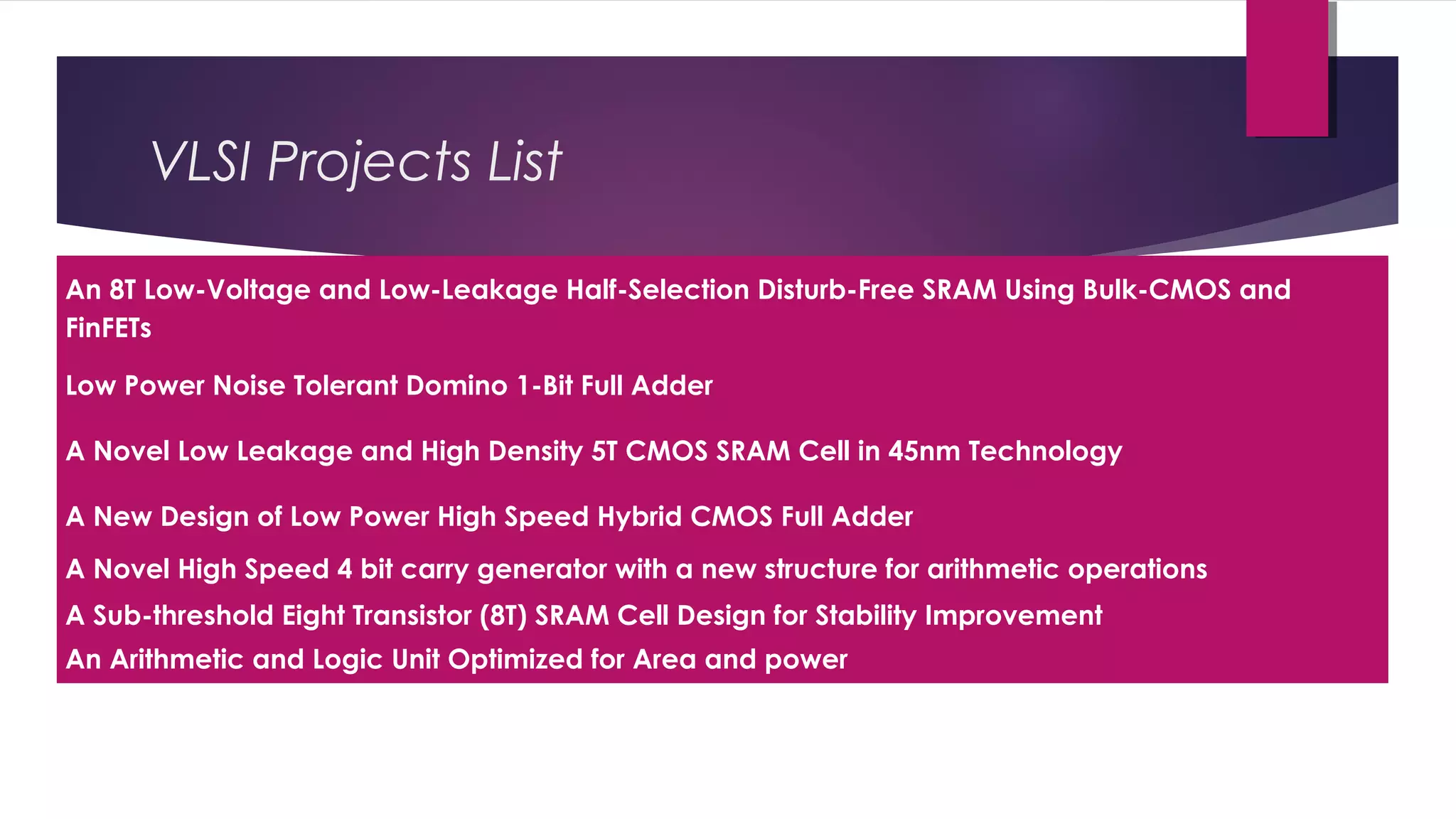
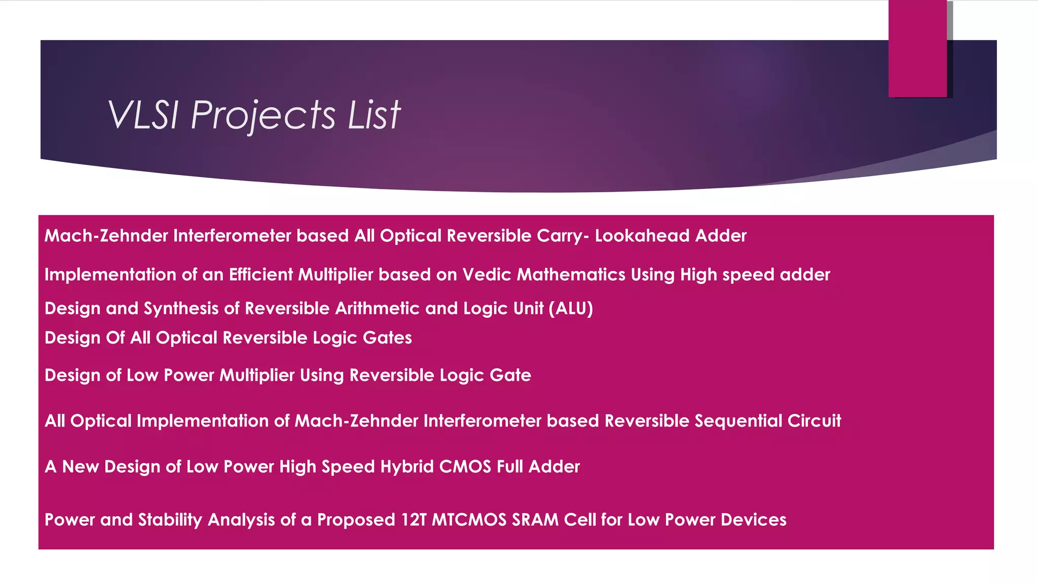
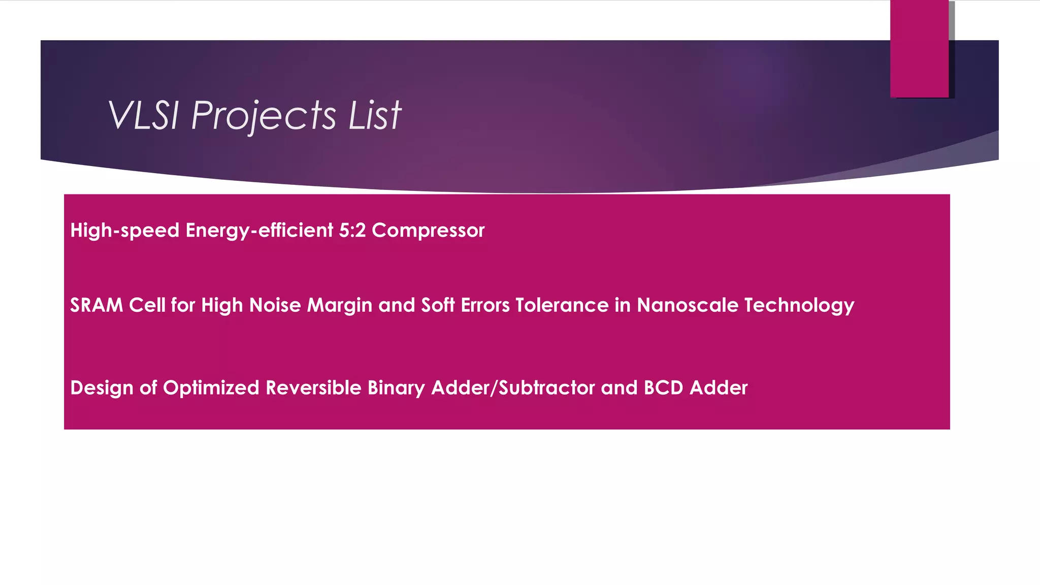
VLSI Projects List
E2MATRIX RESEARCH LAB
OPP PHAGWARA BUS STAND, PARMAR COMPLEX, BACKSIDE AXIS BANK.
PHAGWARA, PUNJAB ( INDIA )
VLSI Projects
 VLSI stands for Very Large Scale Integration. Generally there are
mainly 2 types of VLSI projects – 1. Projects in VLSI based System
Design, 2. VLSI Design Projects. You might be confused to
understand the difference between these 2 types of projects. Let
me now explain to you.
 Projects in VLSI based system design are the projects which involve
the design of various types of digital systems that can be
implemented on a PLD device like a FPGA or a CPLD.
 The projects which deal with the semiconductor design are called as
Projects in VLSI design. These are very difficult and expensive to implement
in real time.
VLSI Projects
 We have already seen the following engineering project ideas:
 Embedded Systems Projects
 Electronics Projects
 Robotics Projects
VLSI Projects
 So, here we are publishing a list of various VLSI projects which are
very useful for final year engineering students. These VLSI projects
are interesting and helpful in our real life also. You may just go
through this list of projects and get good knowledge on VLSI
projects.
VLSI Projects
Design and Estimation of delay, power and area for Parallel prefix adders
Detection of Hardware Trojan in SEA Using Path Delay
parallel multiplier accumulator Based on radix-2 Modified Booth Algorithm by using a VLSI
architecture
Area–Delay–Power Efficient Carry-Select Adder
Realization of 2:4 reversible decoder and its applications
All Optical Reversible Multiplexer Design using Mach-Zehnder interferometer
Design of Dedicated Reversible Quantum Circuitry for Square Computation
Approach to design a compact reversible low power binary comparator
VLSI Projects List
Recursive Approach to the Design of a Parallel Self-Timed Adder
Parity Preserving Logic based Fault Tolerant Reversible ALU
An Optimized Design of Binary Comparator Circuit in Quantum Computing
ASIC Design of Reversible Multiplier Circuit
A Low Energy and High Performance DM^2 Adder
Analysis and Design of a Low-Voltage Low-Power Double-Tail Comparator
Low Power Pulse Triggered Flip-Flop Design based on Signal Feed-Through Scheme
Increase in Read Noise Margin of Single-Bit-Line SRAM Using Adiabatic Change of Word Line
Voltage
VLSI Projects List
An 8T Low-Voltage and Low-Leakage Half-Selection Disturb-Free SRAM Using Bulk-CMOS and
FinFETs
Low Power Noise Tolerant Domino 1-Bit Full Adder
A Novel Low Leakage and High Density 5T CMOS SRAM Cell in 45nm Technology
A New Design of Low Power High Speed Hybrid CMOS Full Adder
A Novel High Speed 4 bit carry generator with a new structure for arithmetic operations
A Sub-threshold Eight Transistor (8T) SRAM Cell Design for Stability Improvement
An Arithmetic and Logic Unit Optimized for Area and power
VLSI Projects List
Mach-Zehnder Interferometer based All Optical Reversible Carry- Lookahead Adder
Implementation of an Efficient Multiplier based on Vedic Mathematics Using High speed adder
Design and Synthesis of Reversible Arithmetic and Logic Unit (ALU)
Design Of All Optical Reversible Logic Gates
Design of Low Power Multiplier Using Reversible Logic Gate
All Optical Implementation of Mach-Zehnder Interferometer based Reversible Sequential Circuit
A New Design of Low Power High Speed Hybrid CMOS Full Adder
Power and Stability Analysis of a Proposed 12T MTCMOS SRAM Cell for Low Power Devices
VLSI Projects List
High-speed Energy-efficient 5:2 Compressor
SRAM Cell for High Noise Margin and Soft Errors Tolerance in Nanoscale Technology
Design of Optimized Reversible Binary Adder/Subtractor and BCD Adder
VLSI Projects List
E2MATRIX Research Lab
Opp Phagwara Bus Stand, Parmar Complex
Backside Axis Bank, Phagwara
Punjab ( INDIA ).
Website : www.e2matrix.com
Email ID : support@e2matrix.com

VLSI Projects Titles

  • 1.
    VLSI Projects List E2MATRIXRESEARCH LAB OPP PHAGWARA BUS STAND, PARMAR COMPLEX, BACKSIDE AXIS BANK. PHAGWARA, PUNJAB ( INDIA )
  • 2.
    VLSI Projects  VLSIstands for Very Large Scale Integration. Generally there are mainly 2 types of VLSI projects – 1. Projects in VLSI based System Design, 2. VLSI Design Projects. You might be confused to understand the difference between these 2 types of projects. Let me now explain to you.  Projects in VLSI based system design are the projects which involve the design of various types of digital systems that can be implemented on a PLD device like a FPGA or a CPLD.
  • 3.
     The projectswhich deal with the semiconductor design are called as Projects in VLSI design. These are very difficult and expensive to implement in real time. VLSI Projects
  • 4.
     We havealready seen the following engineering project ideas:  Embedded Systems Projects  Electronics Projects  Robotics Projects VLSI Projects
  • 5.
     So, herewe are publishing a list of various VLSI projects which are very useful for final year engineering students. These VLSI projects are interesting and helpful in our real life also. You may just go through this list of projects and get good knowledge on VLSI projects. VLSI Projects
  • 6.
    Design and Estimationof delay, power and area for Parallel prefix adders Detection of Hardware Trojan in SEA Using Path Delay parallel multiplier accumulator Based on radix-2 Modified Booth Algorithm by using a VLSI architecture Area–Delay–Power Efficient Carry-Select Adder Realization of 2:4 reversible decoder and its applications All Optical Reversible Multiplexer Design using Mach-Zehnder interferometer Design of Dedicated Reversible Quantum Circuitry for Square Computation Approach to design a compact reversible low power binary comparator VLSI Projects List
  • 7.
    Recursive Approach tothe Design of a Parallel Self-Timed Adder Parity Preserving Logic based Fault Tolerant Reversible ALU An Optimized Design of Binary Comparator Circuit in Quantum Computing ASIC Design of Reversible Multiplier Circuit A Low Energy and High Performance DM^2 Adder Analysis and Design of a Low-Voltage Low-Power Double-Tail Comparator Low Power Pulse Triggered Flip-Flop Design based on Signal Feed-Through Scheme Increase in Read Noise Margin of Single-Bit-Line SRAM Using Adiabatic Change of Word Line Voltage VLSI Projects List
  • 8.
    An 8T Low-Voltageand Low-Leakage Half-Selection Disturb-Free SRAM Using Bulk-CMOS and FinFETs Low Power Noise Tolerant Domino 1-Bit Full Adder A Novel Low Leakage and High Density 5T CMOS SRAM Cell in 45nm Technology A New Design of Low Power High Speed Hybrid CMOS Full Adder A Novel High Speed 4 bit carry generator with a new structure for arithmetic operations A Sub-threshold Eight Transistor (8T) SRAM Cell Design for Stability Improvement An Arithmetic and Logic Unit Optimized for Area and power VLSI Projects List
  • 9.
    Mach-Zehnder Interferometer basedAll Optical Reversible Carry- Lookahead Adder Implementation of an Efficient Multiplier based on Vedic Mathematics Using High speed adder Design and Synthesis of Reversible Arithmetic and Logic Unit (ALU) Design Of All Optical Reversible Logic Gates Design of Low Power Multiplier Using Reversible Logic Gate All Optical Implementation of Mach-Zehnder Interferometer based Reversible Sequential Circuit A New Design of Low Power High Speed Hybrid CMOS Full Adder Power and Stability Analysis of a Proposed 12T MTCMOS SRAM Cell for Low Power Devices VLSI Projects List
  • 10.
    High-speed Energy-efficient 5:2Compressor SRAM Cell for High Noise Margin and Soft Errors Tolerance in Nanoscale Technology Design of Optimized Reversible Binary Adder/Subtractor and BCD Adder VLSI Projects List
  • 11.
    E2MATRIX Research Lab OppPhagwara Bus Stand, Parmar Complex Backside Axis Bank, Phagwara Punjab ( INDIA ). Website : www.e2matrix.com Email ID : support@e2matrix.com