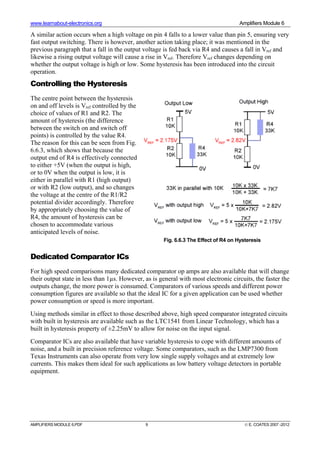
Downloaded 117 times

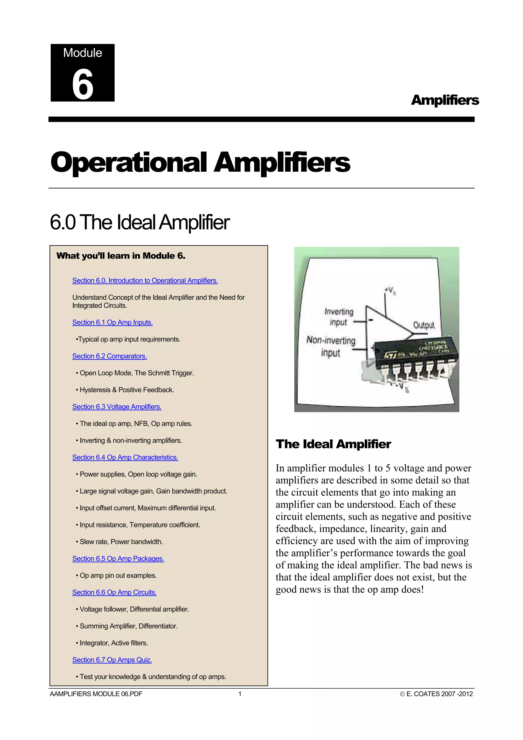
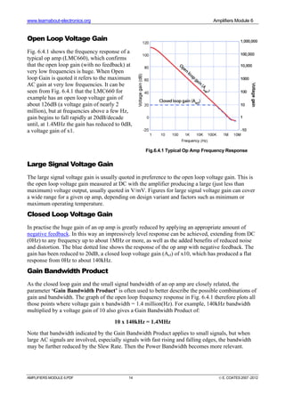

The document discusses the ideal operational amplifier (op amp) and its key properties. It describes how early op amps were developed to provide controllable gain but it was not until integrated circuits that they achieved high performance, small size, and low cost. The ideal op amp would have infinite bandwidth, gain, linearity, and signal-to-noise ratio while being easily configurable and inexpensive. Real op amps approach these ideals using high gain negative feedback configurations. Op amps operate as difference amplifiers, amplifying voltage differences between their inputs while rejecting common mode signals on both inputs.


![Circuit Network Analysis - [Chapter5] Transfer function, frequency response, ...](https://cdn.slidesharecdn.com/ss_thumbnails/ch5-150613063859-lva1-app6891-thumbnail.jpg?width=640&height=640&fit=bounds)
![Circuit Network Analysis - [Chapter4] Laplace Transform](https://cdn.slidesharecdn.com/ss_thumbnails/ch4-150613063858-lva1-app6891-thumbnail.jpg?width=640&height=640&fit=bounds)


