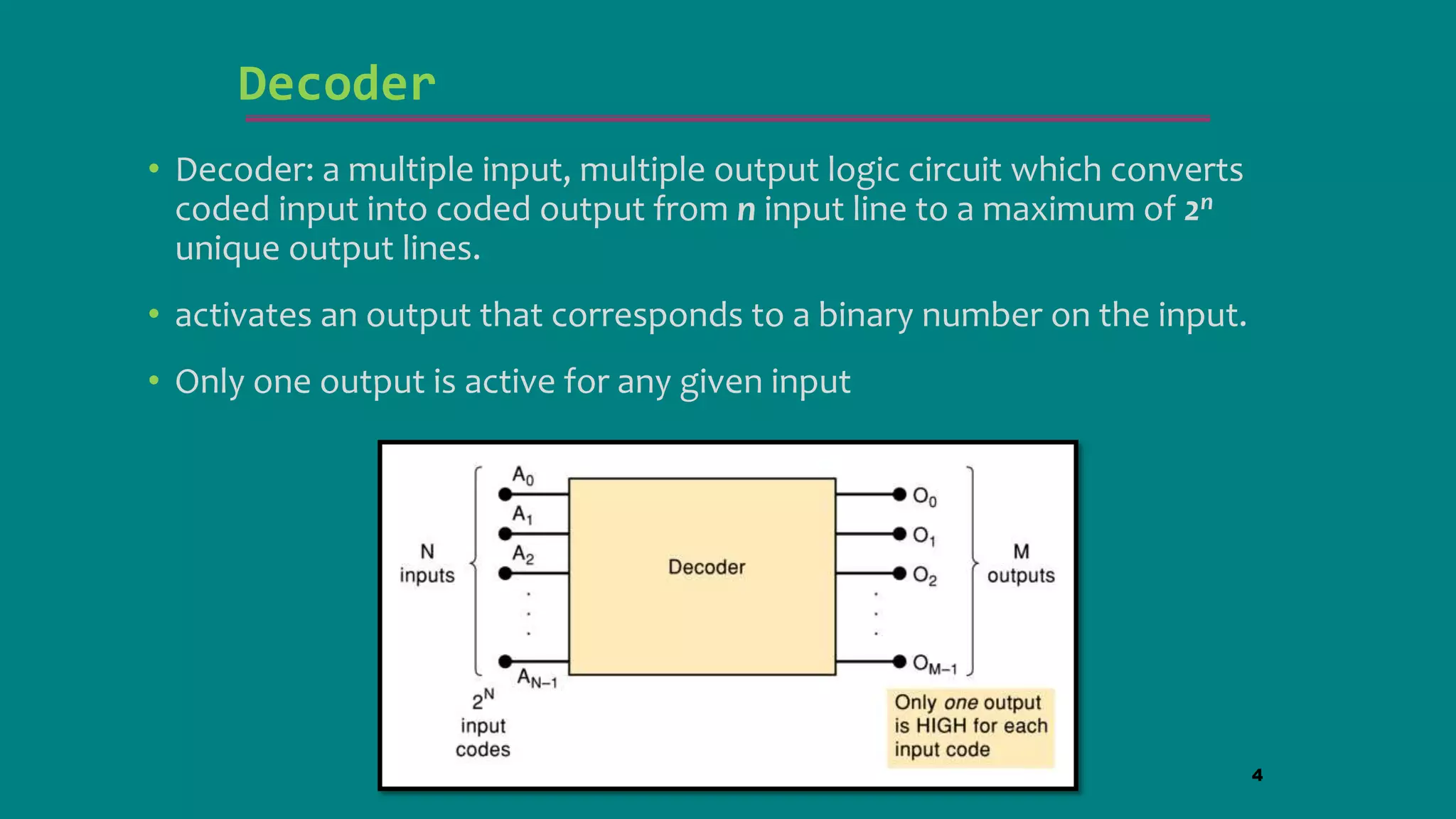
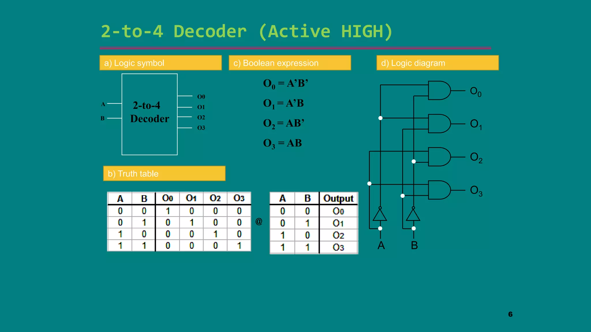
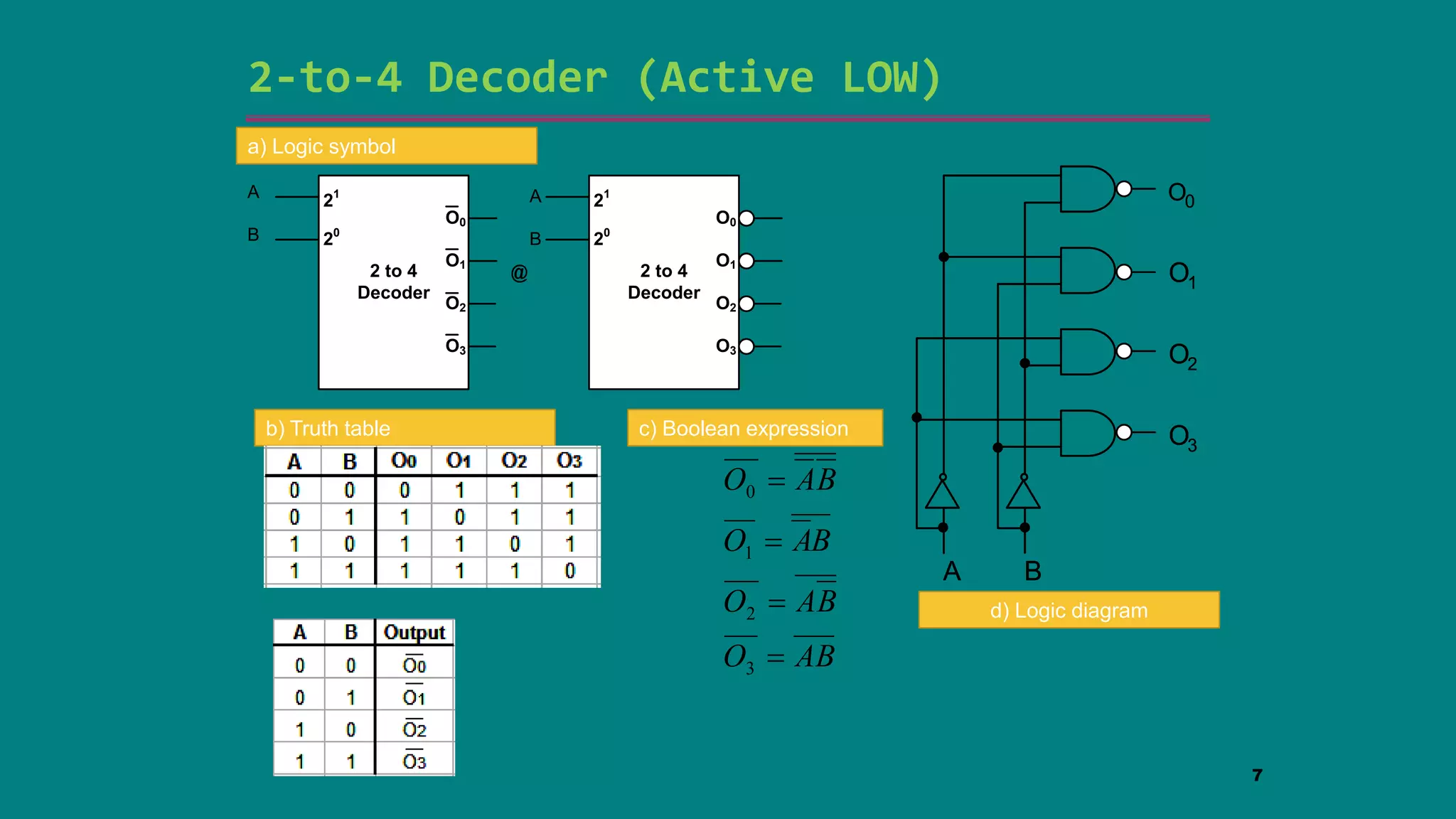
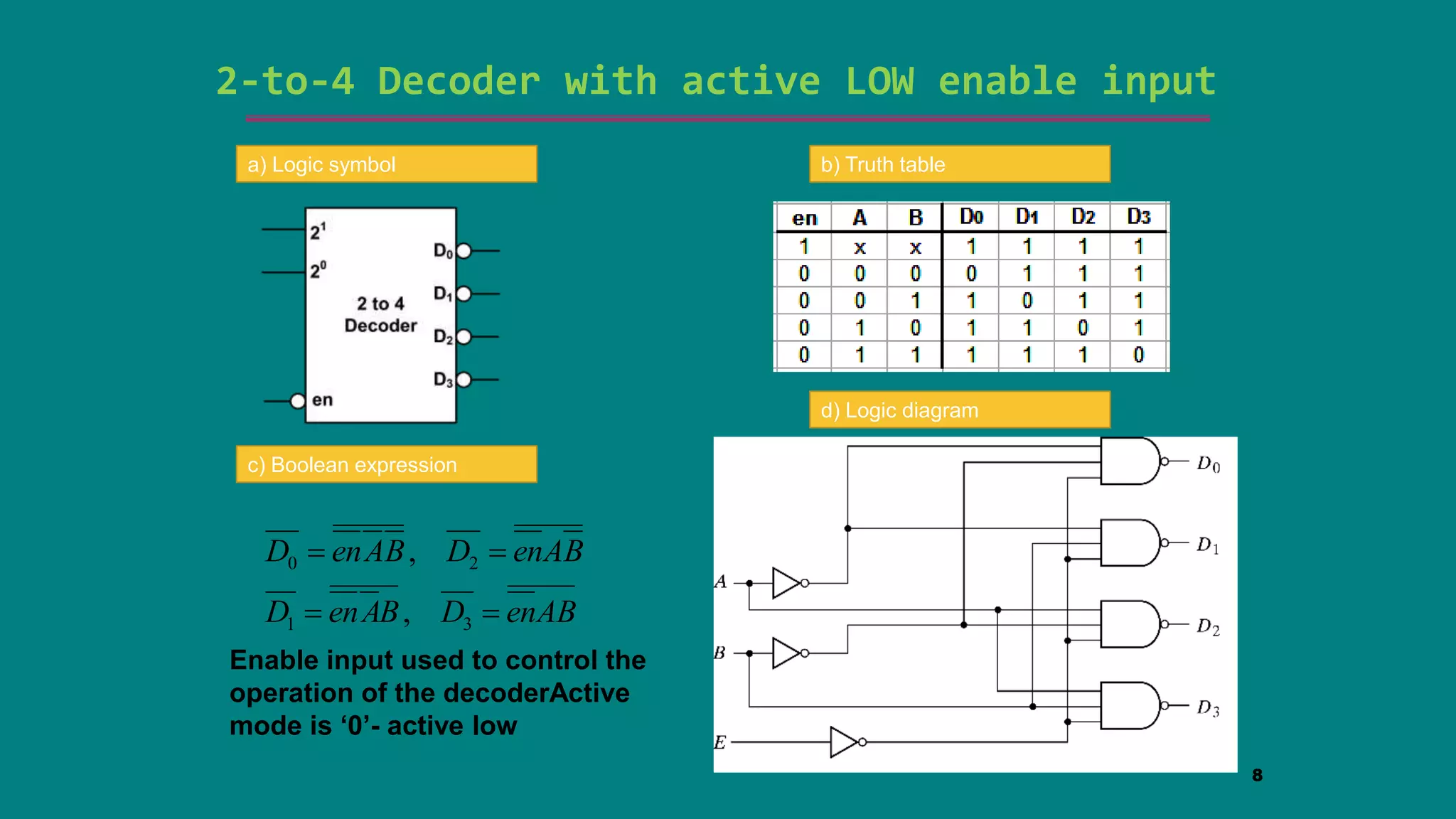
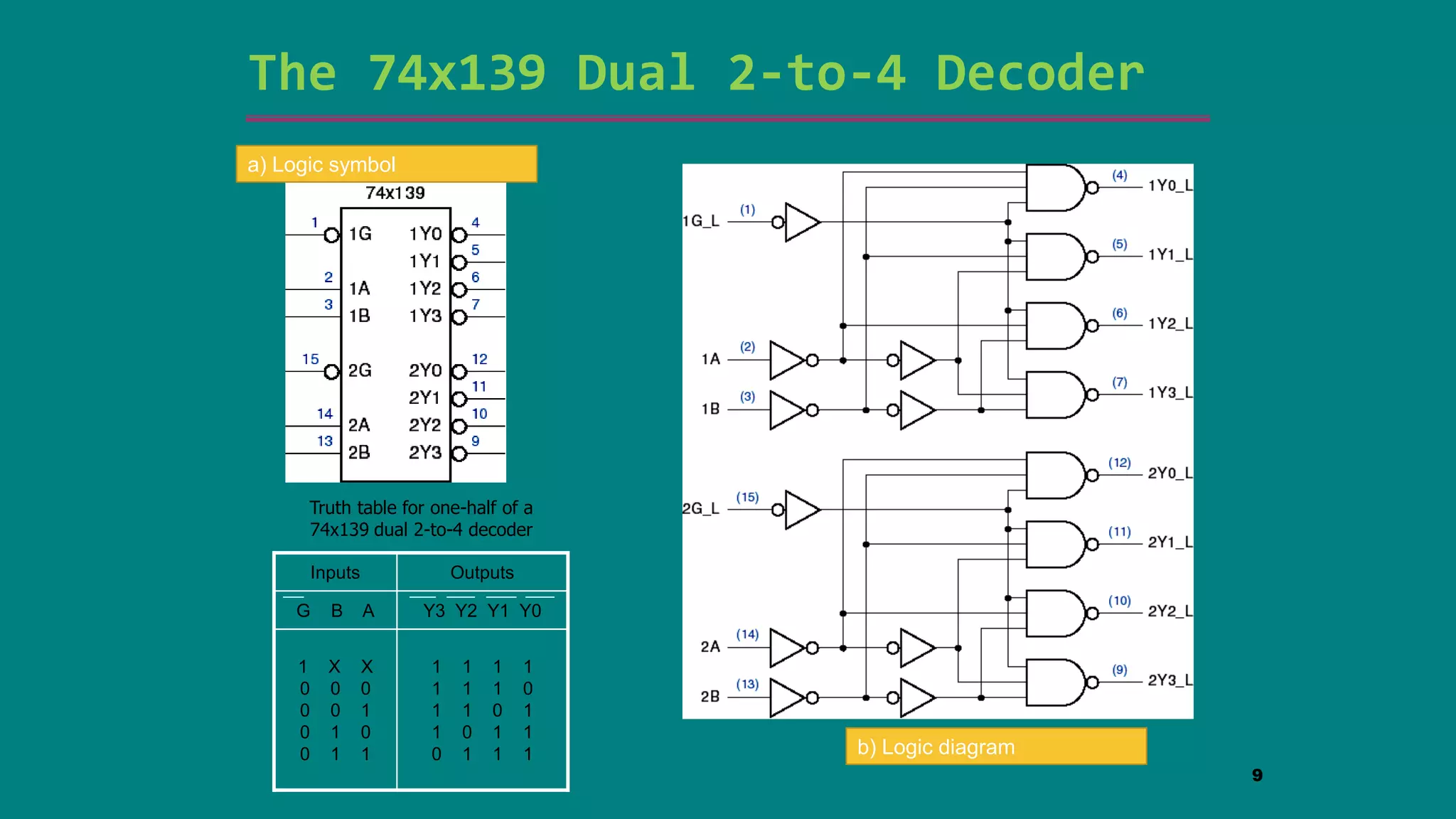
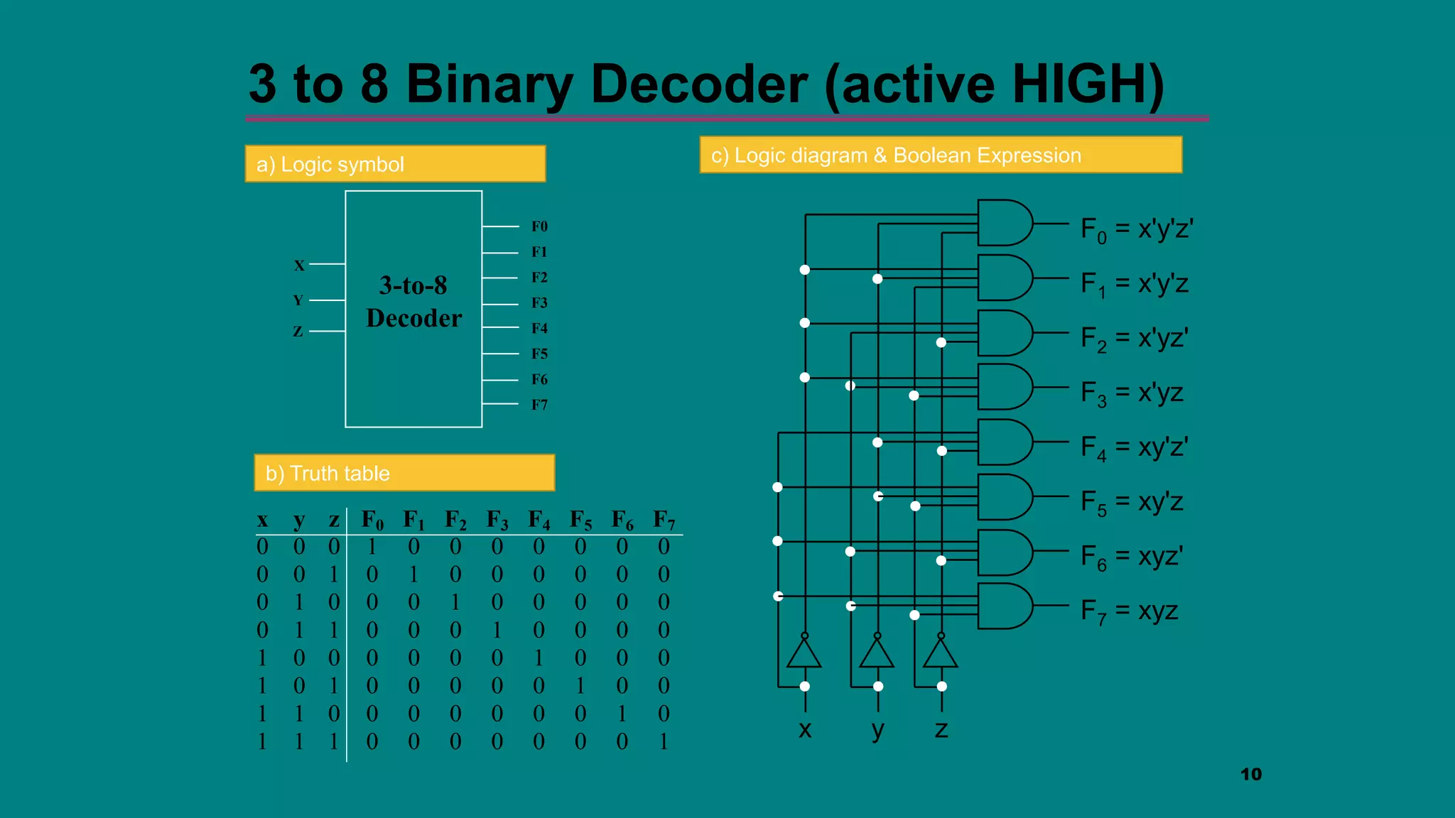
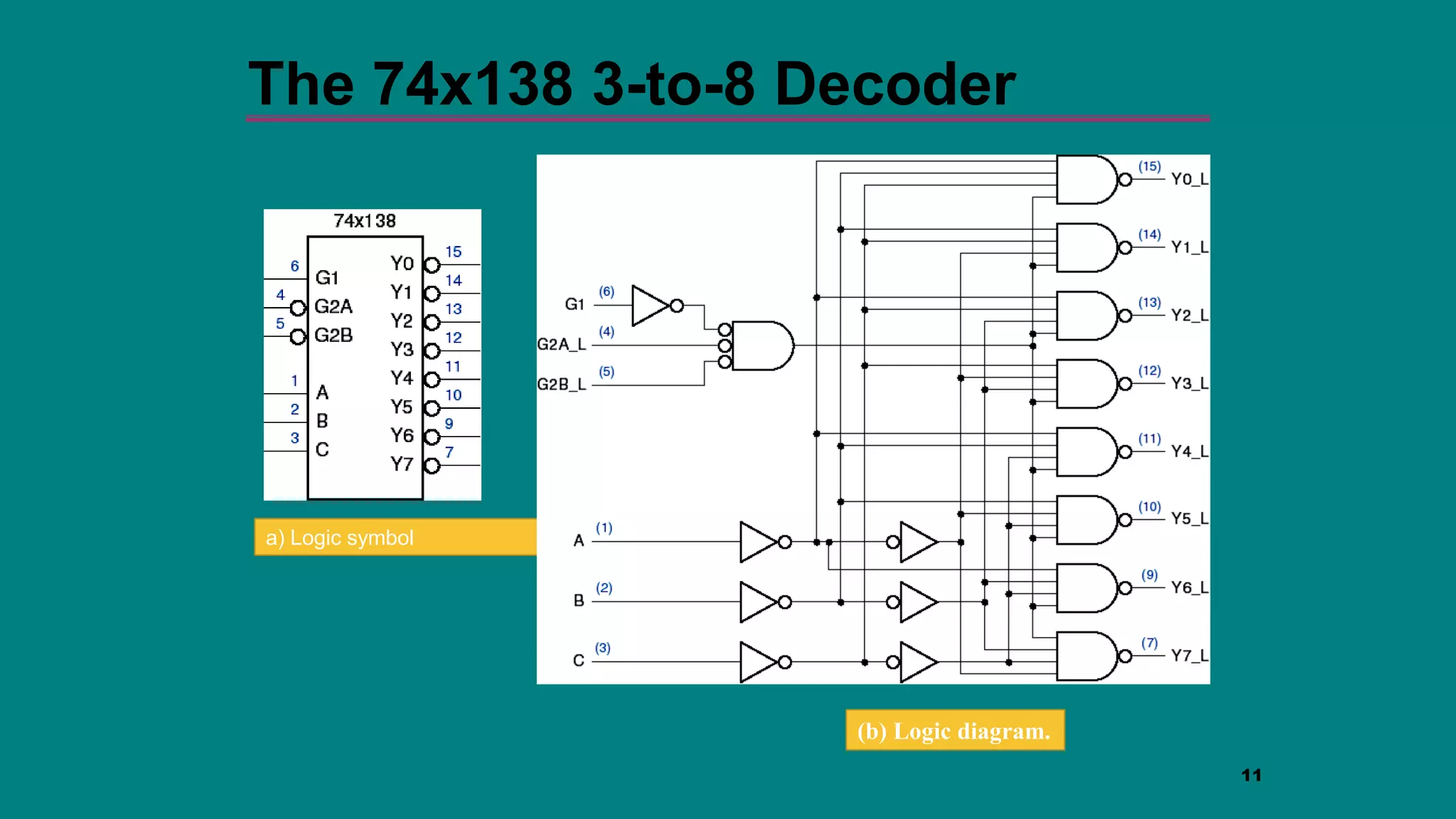
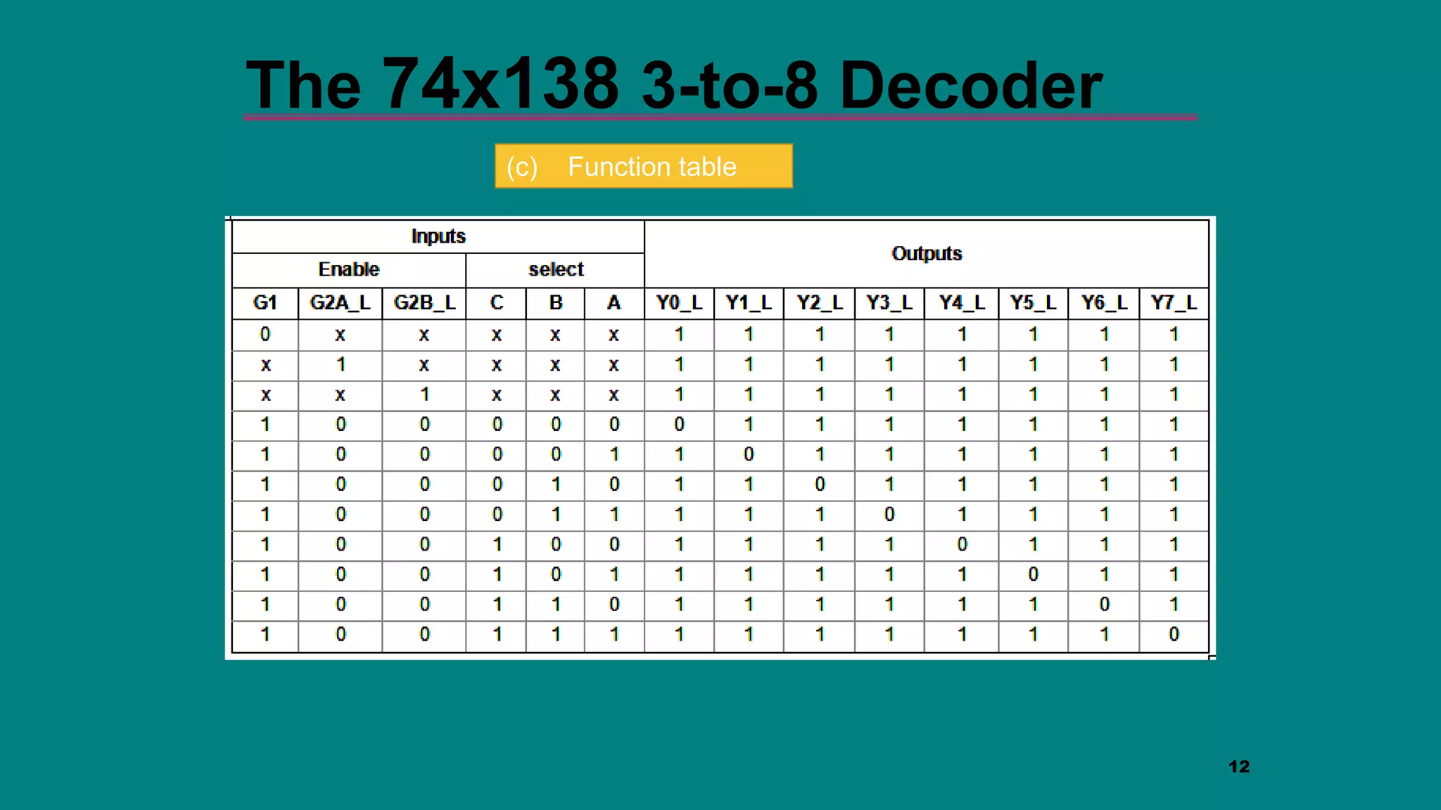
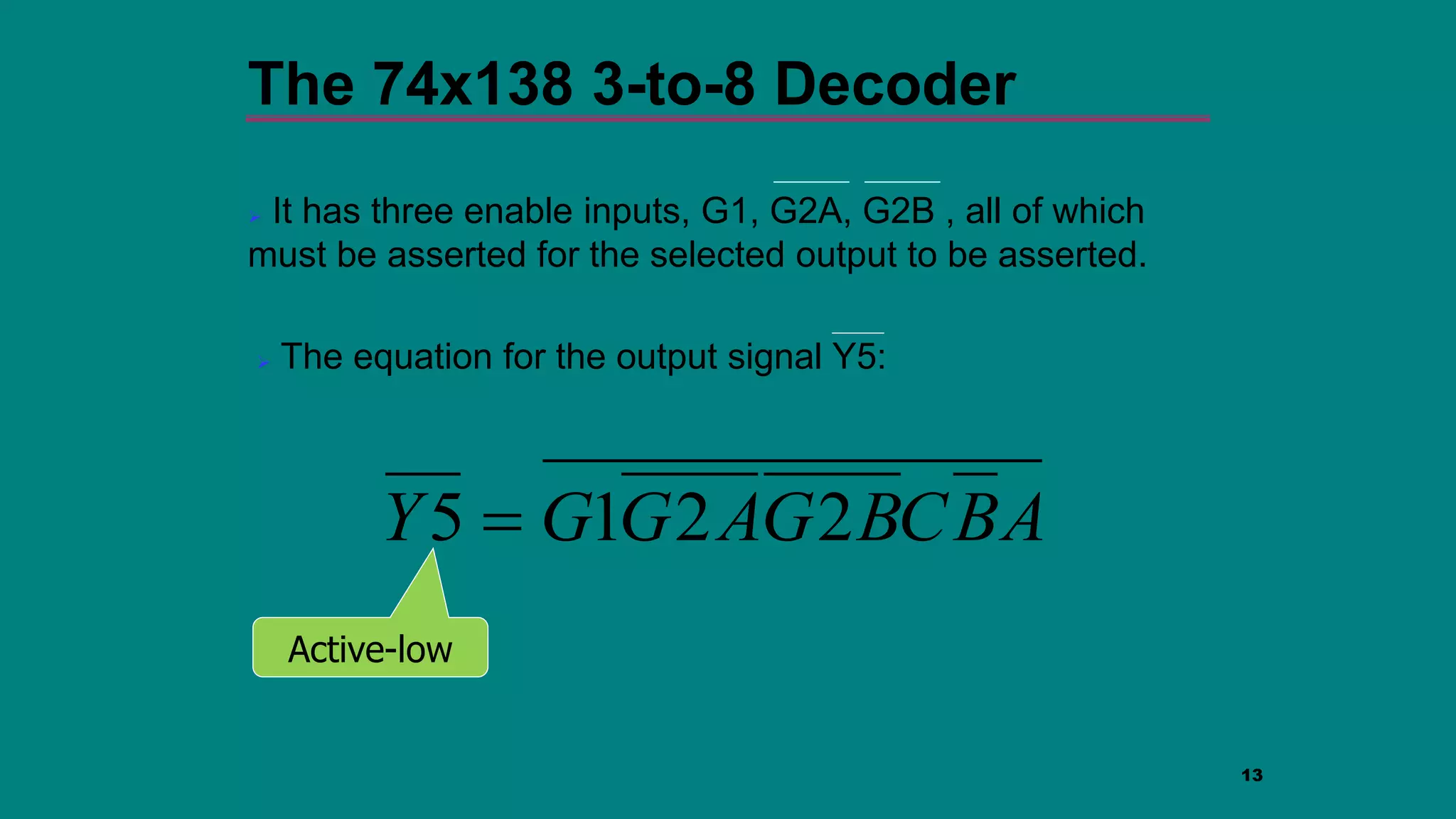
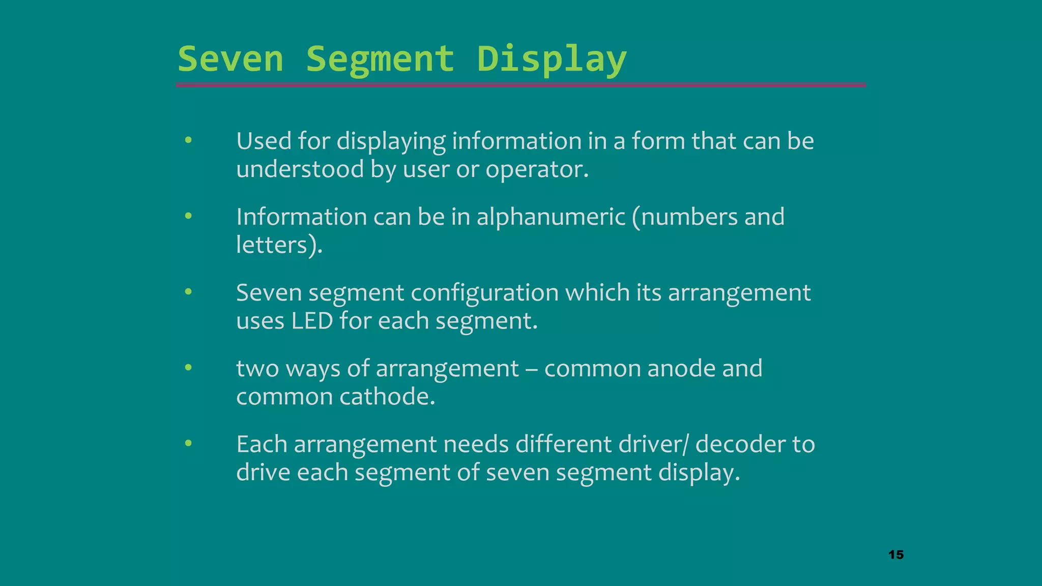
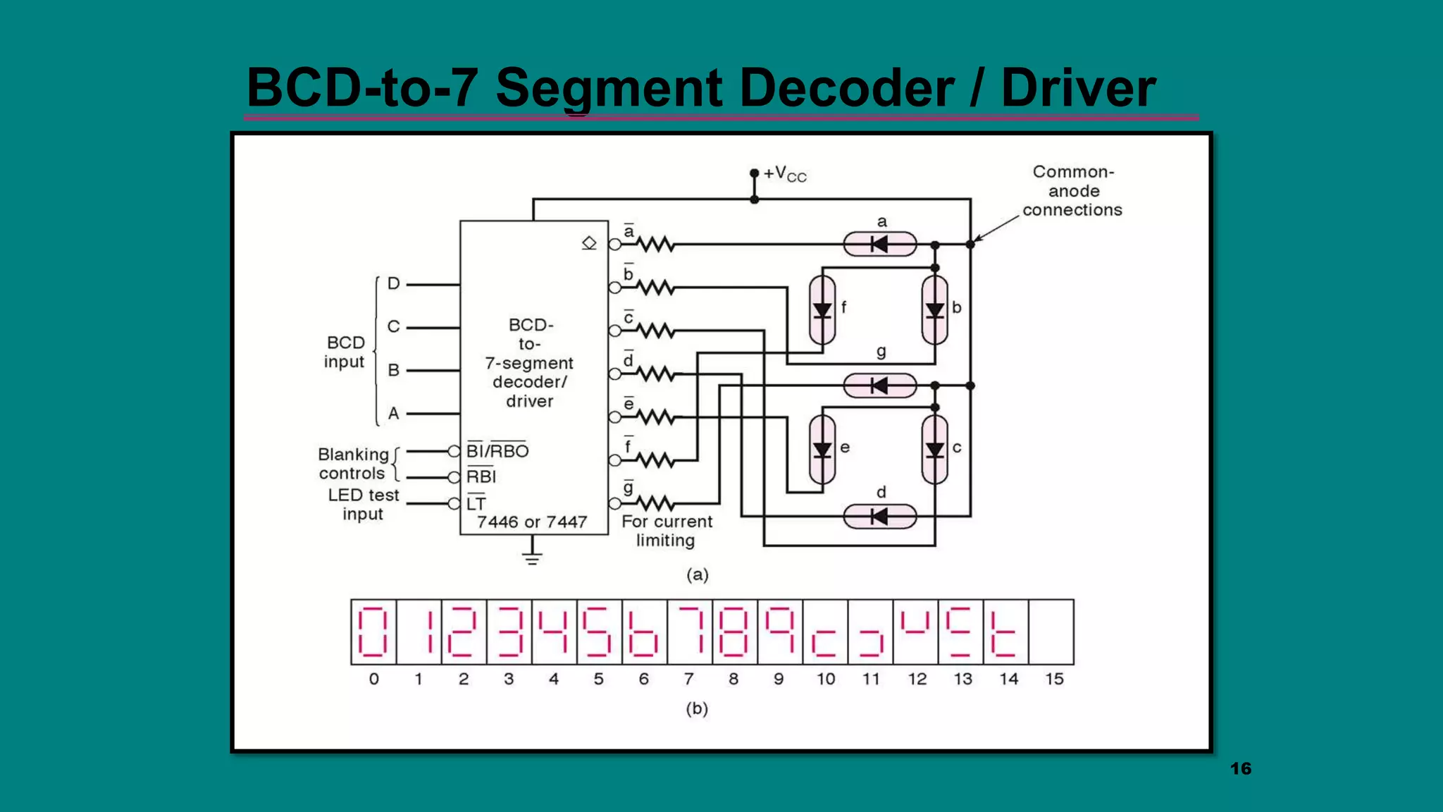
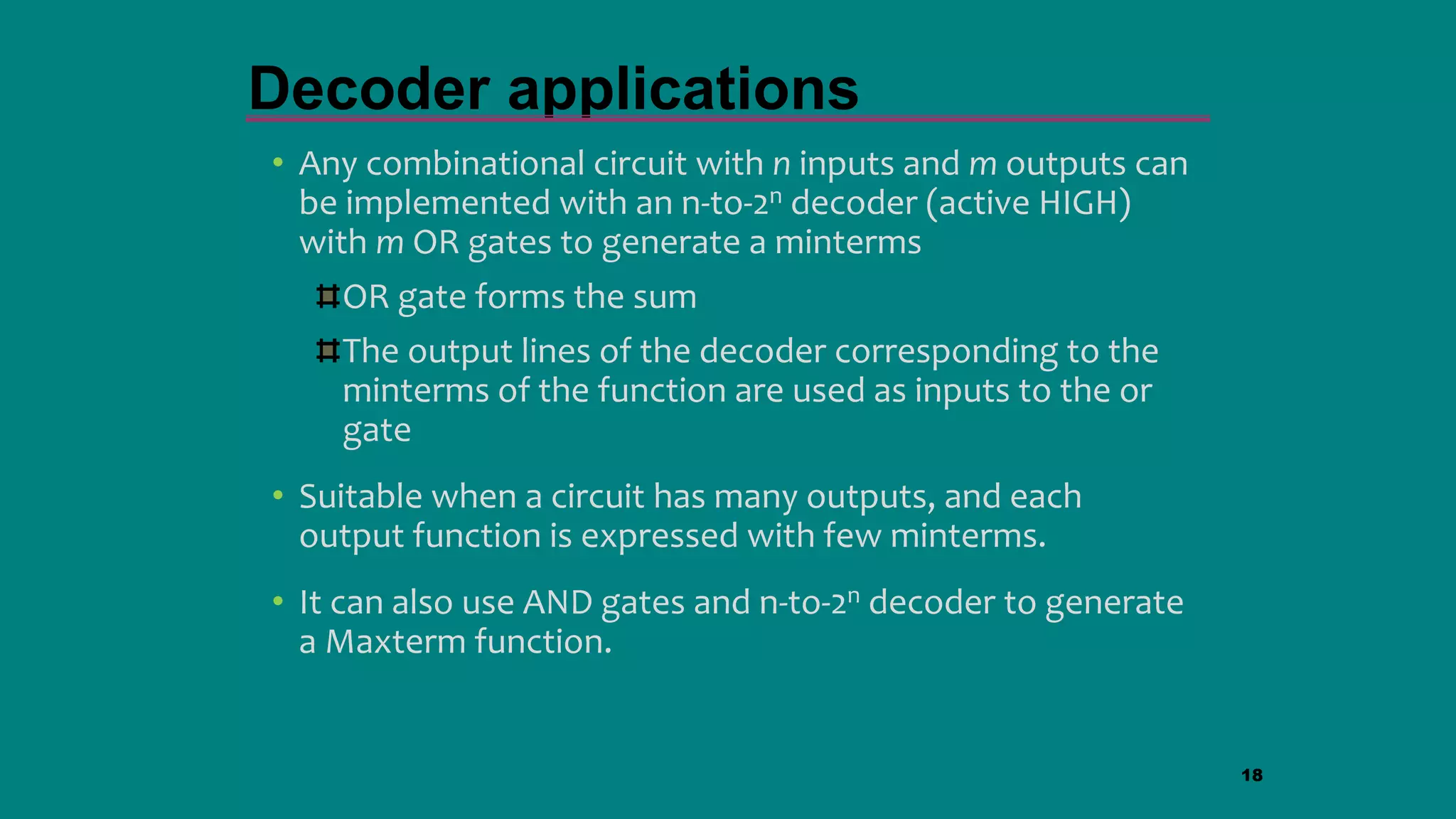
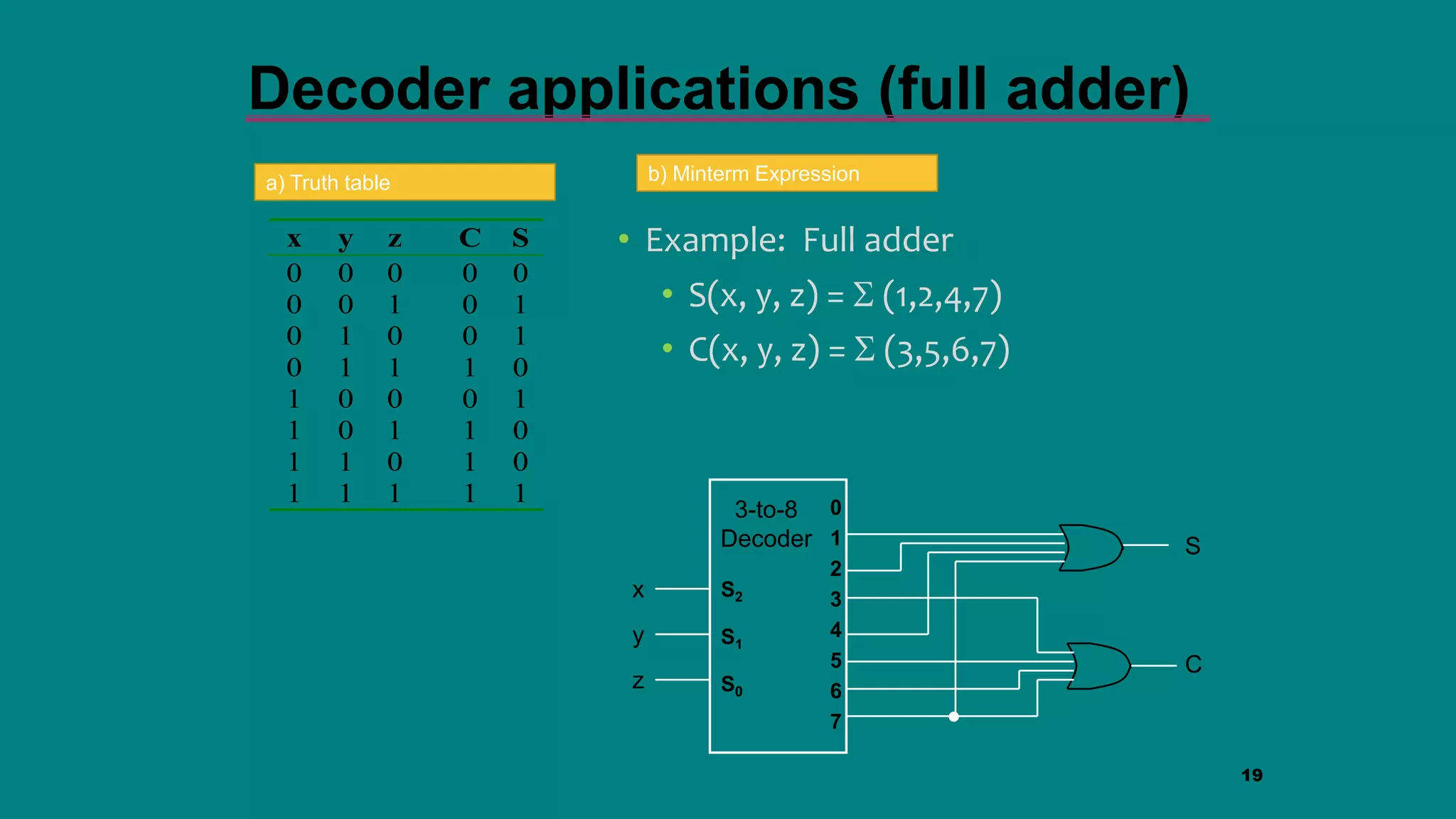
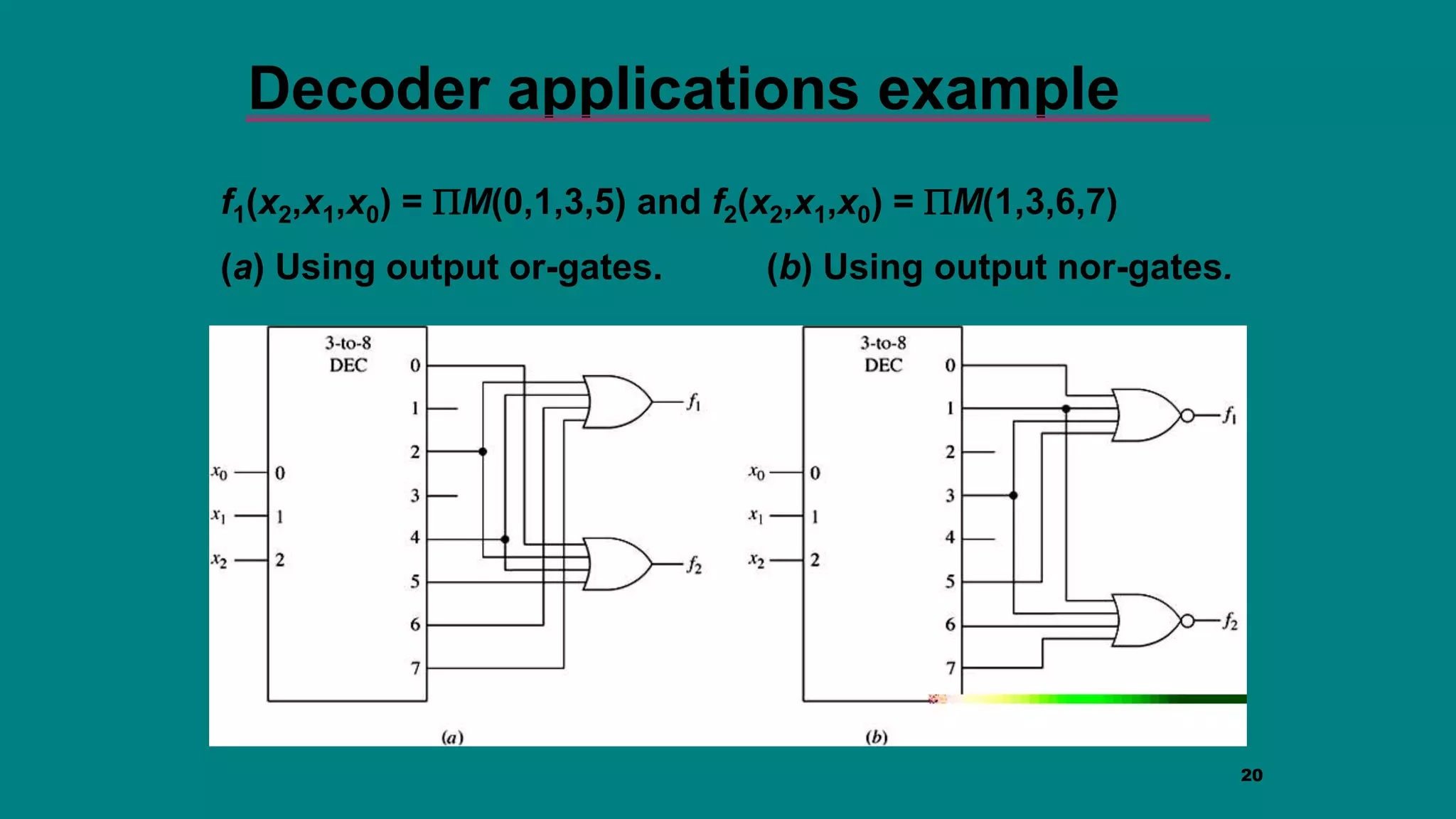
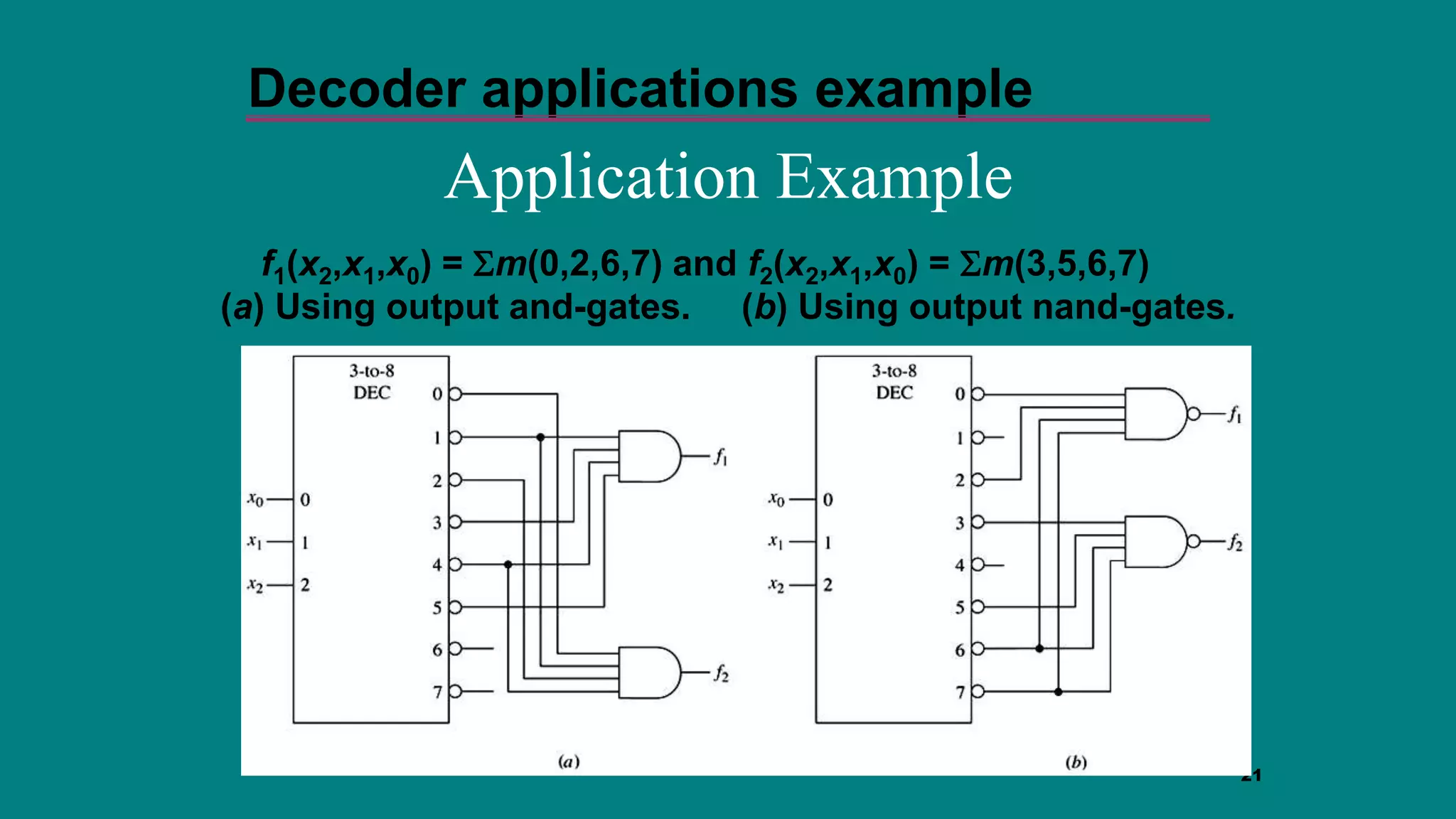
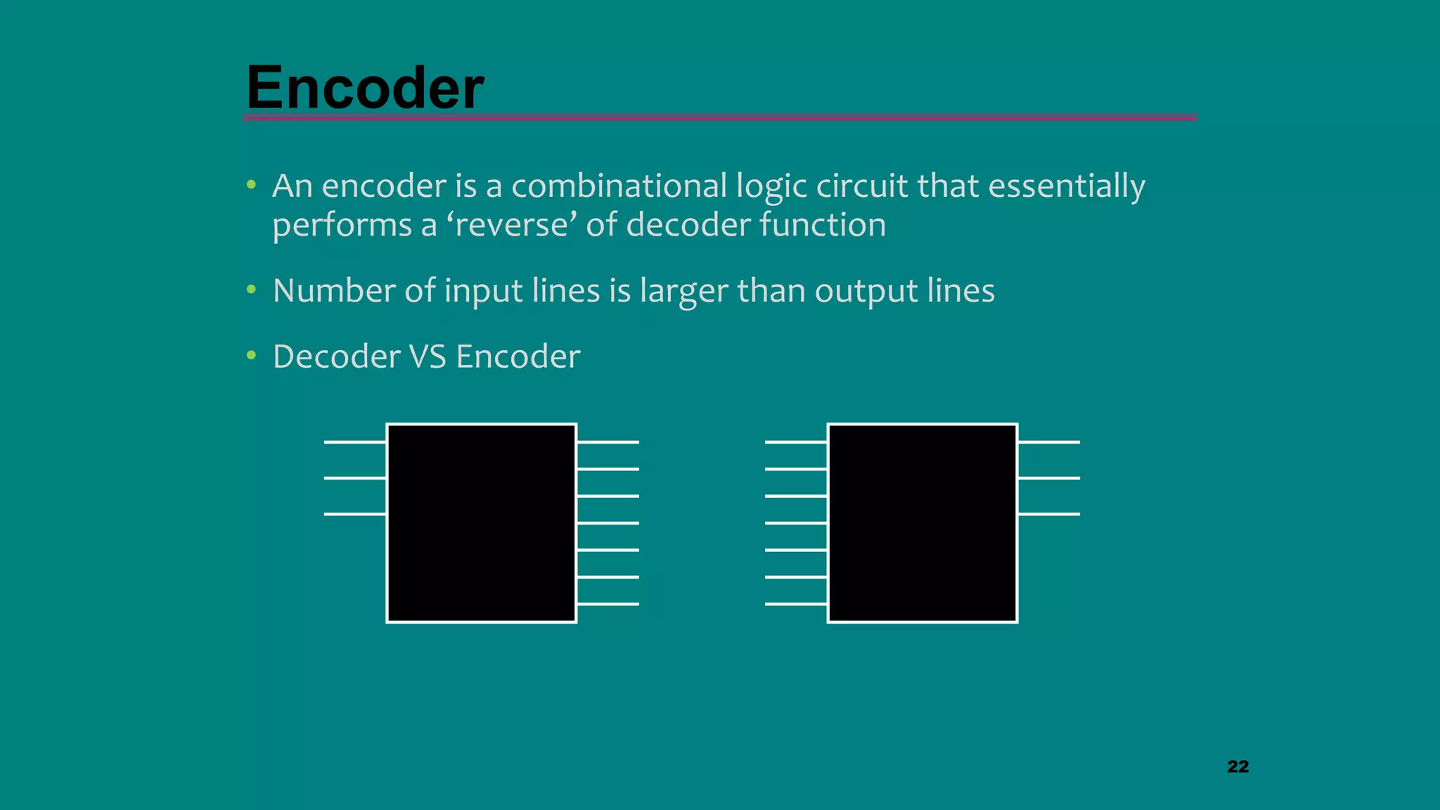
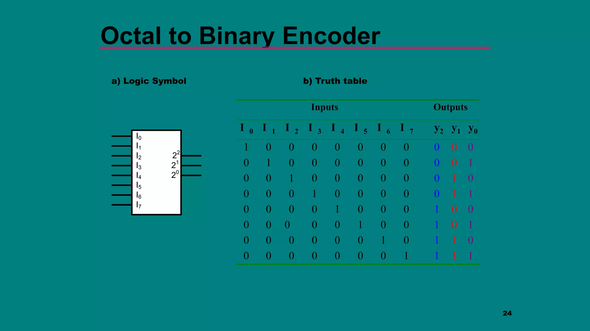
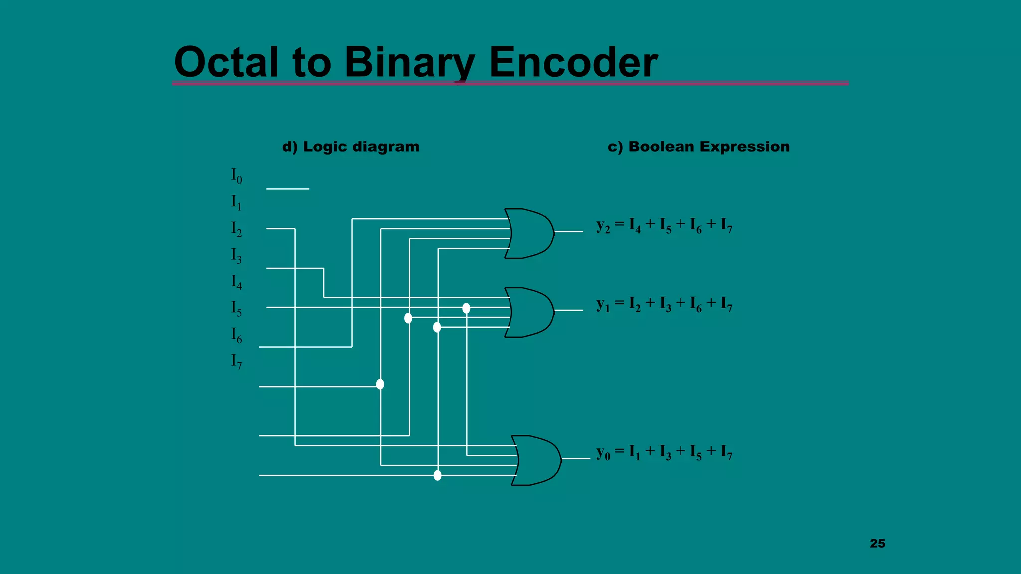
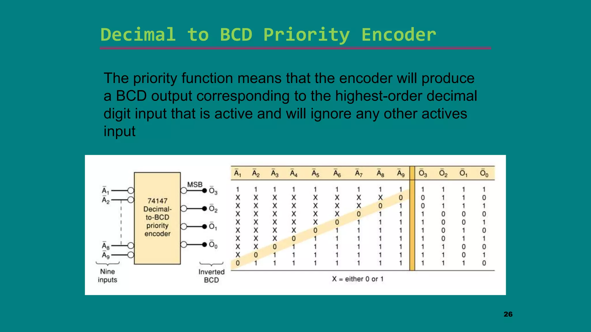
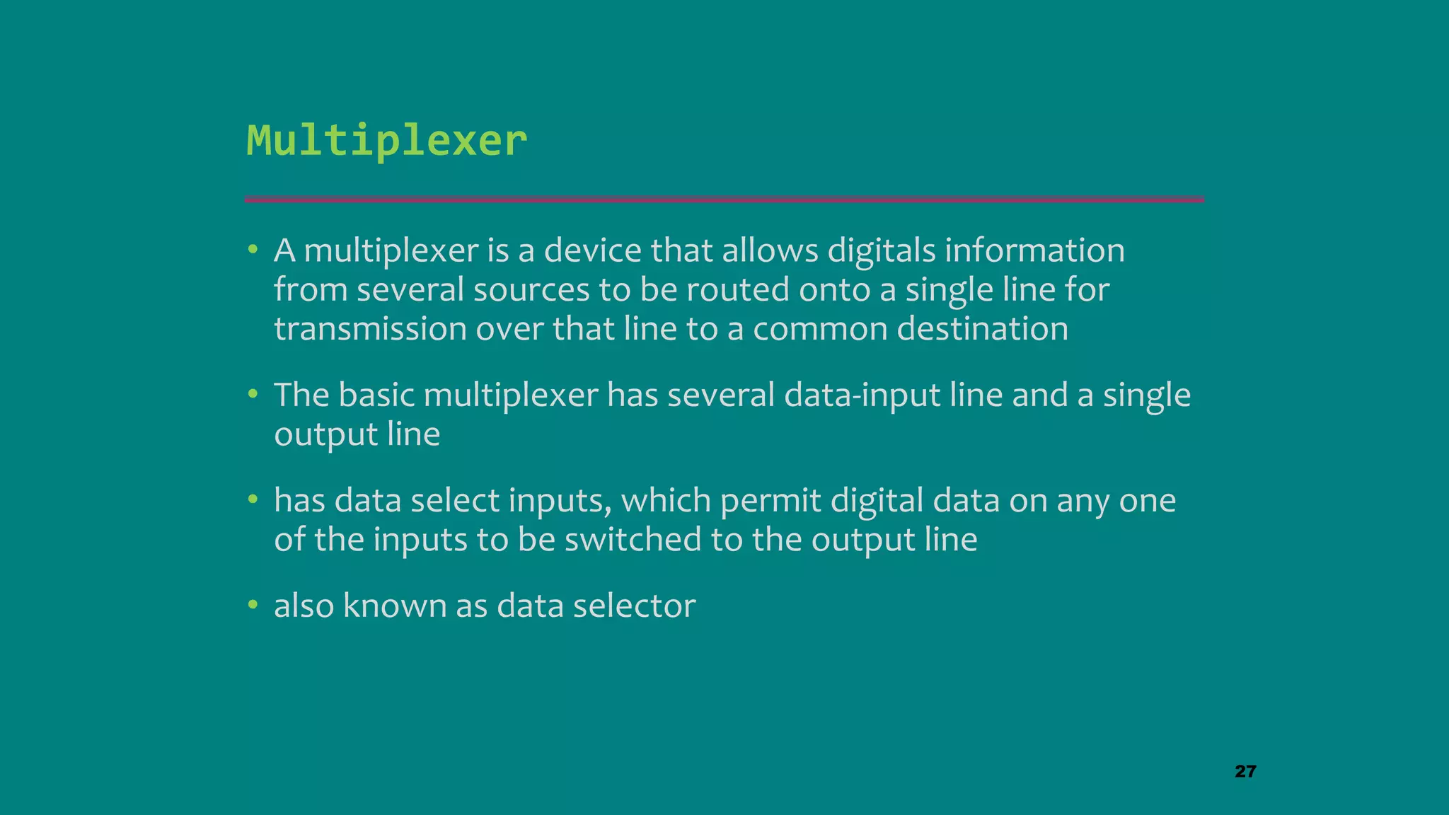
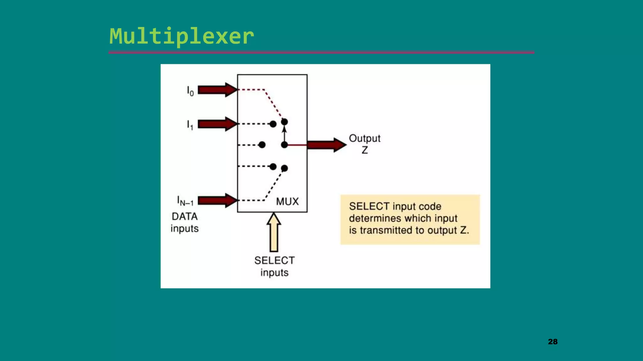
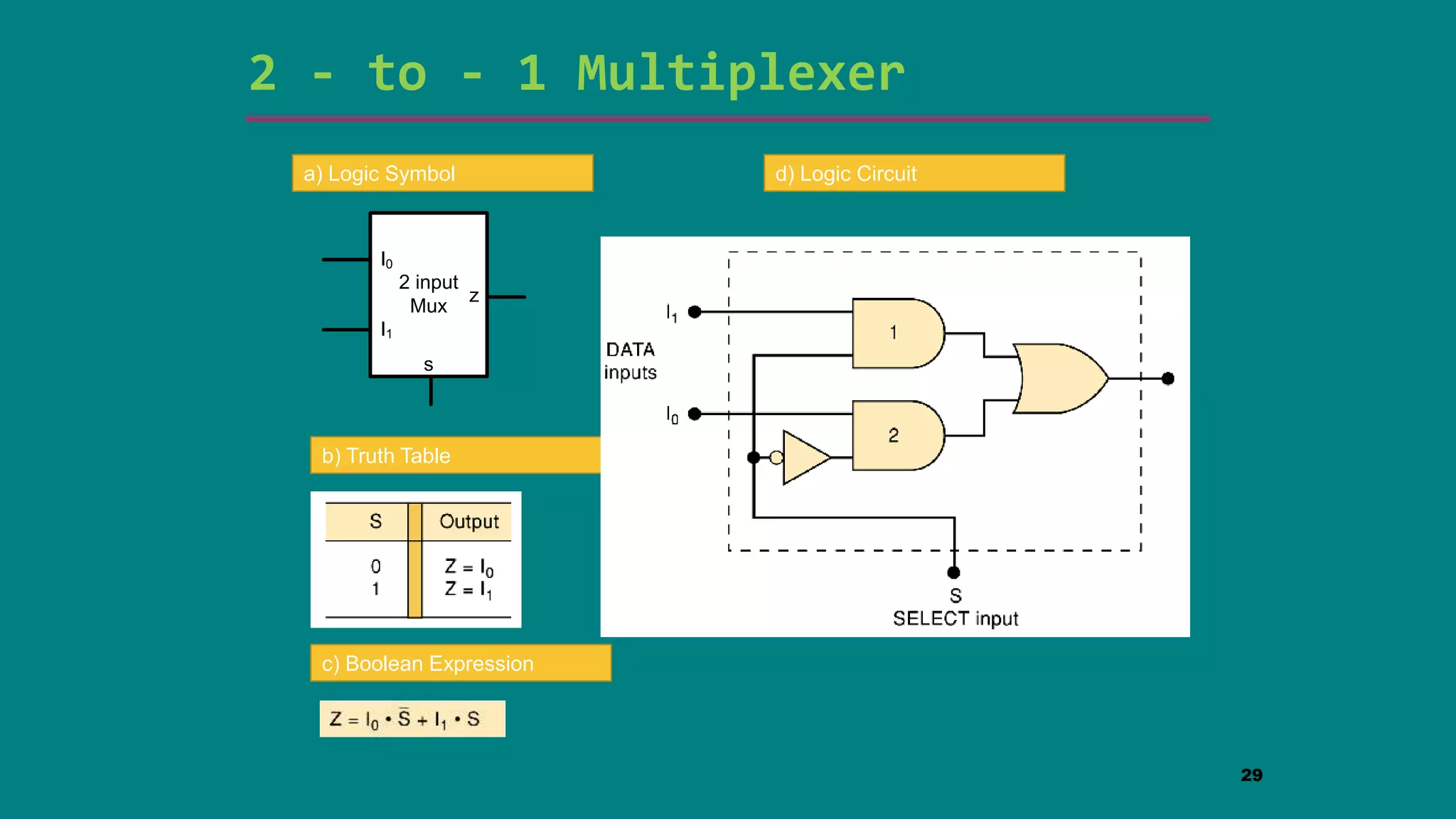
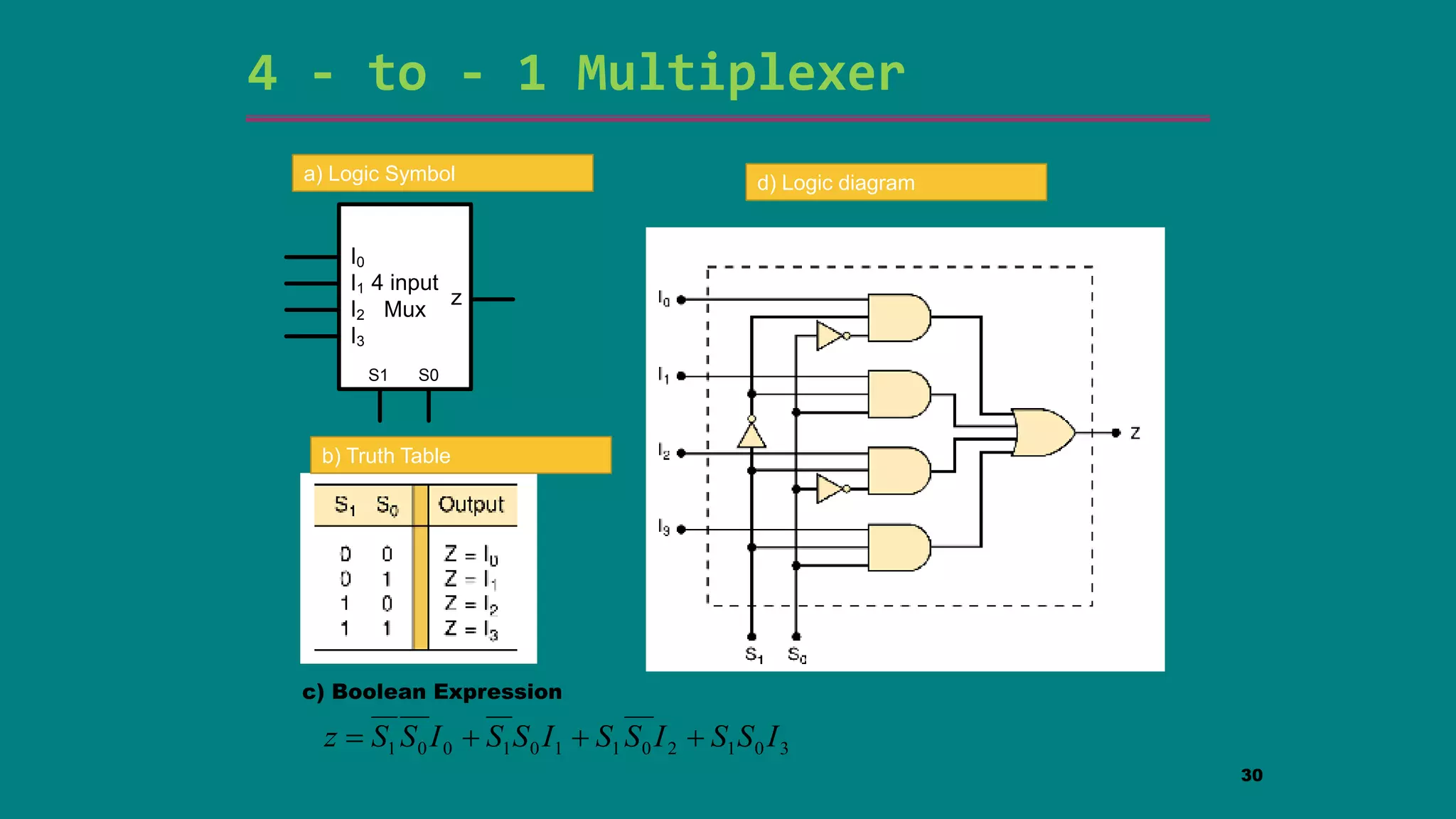
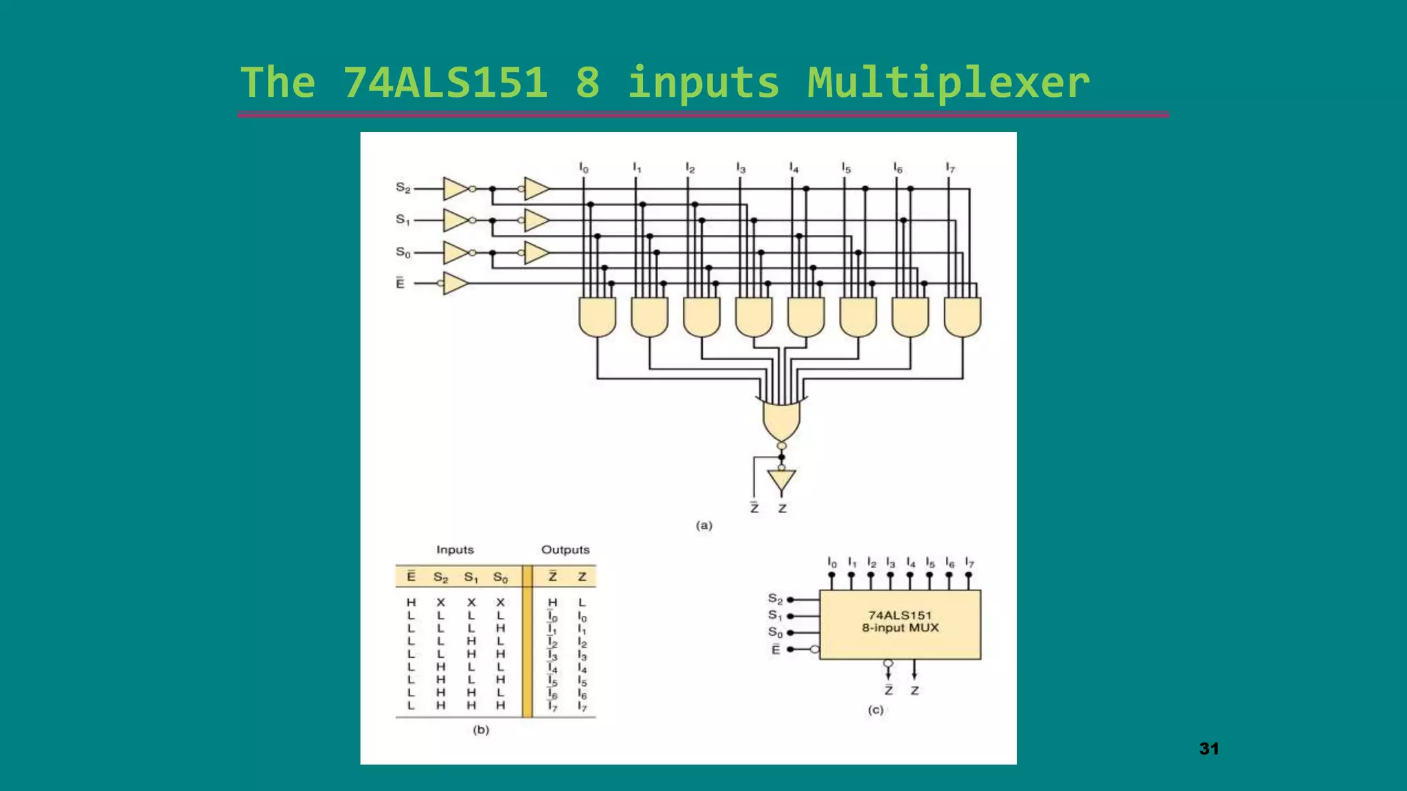
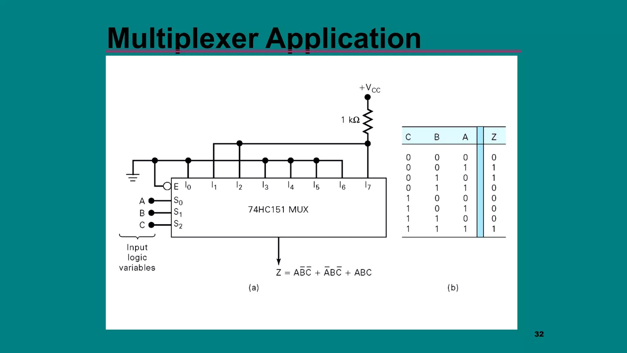
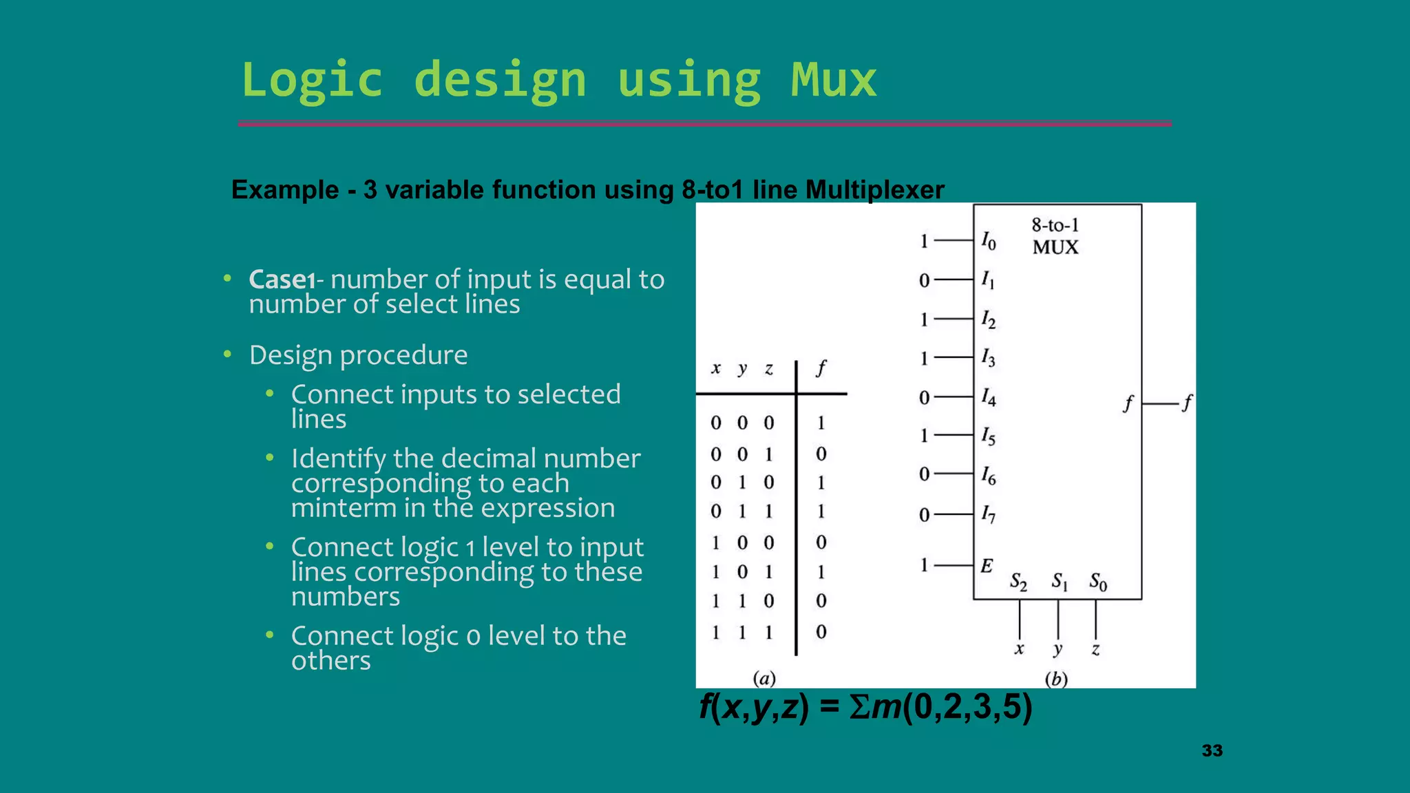
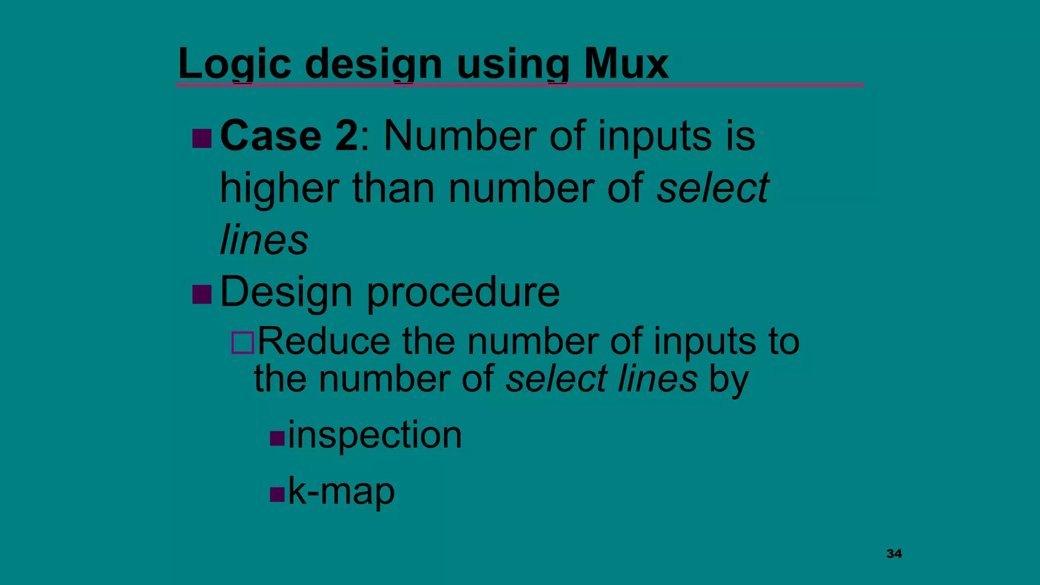
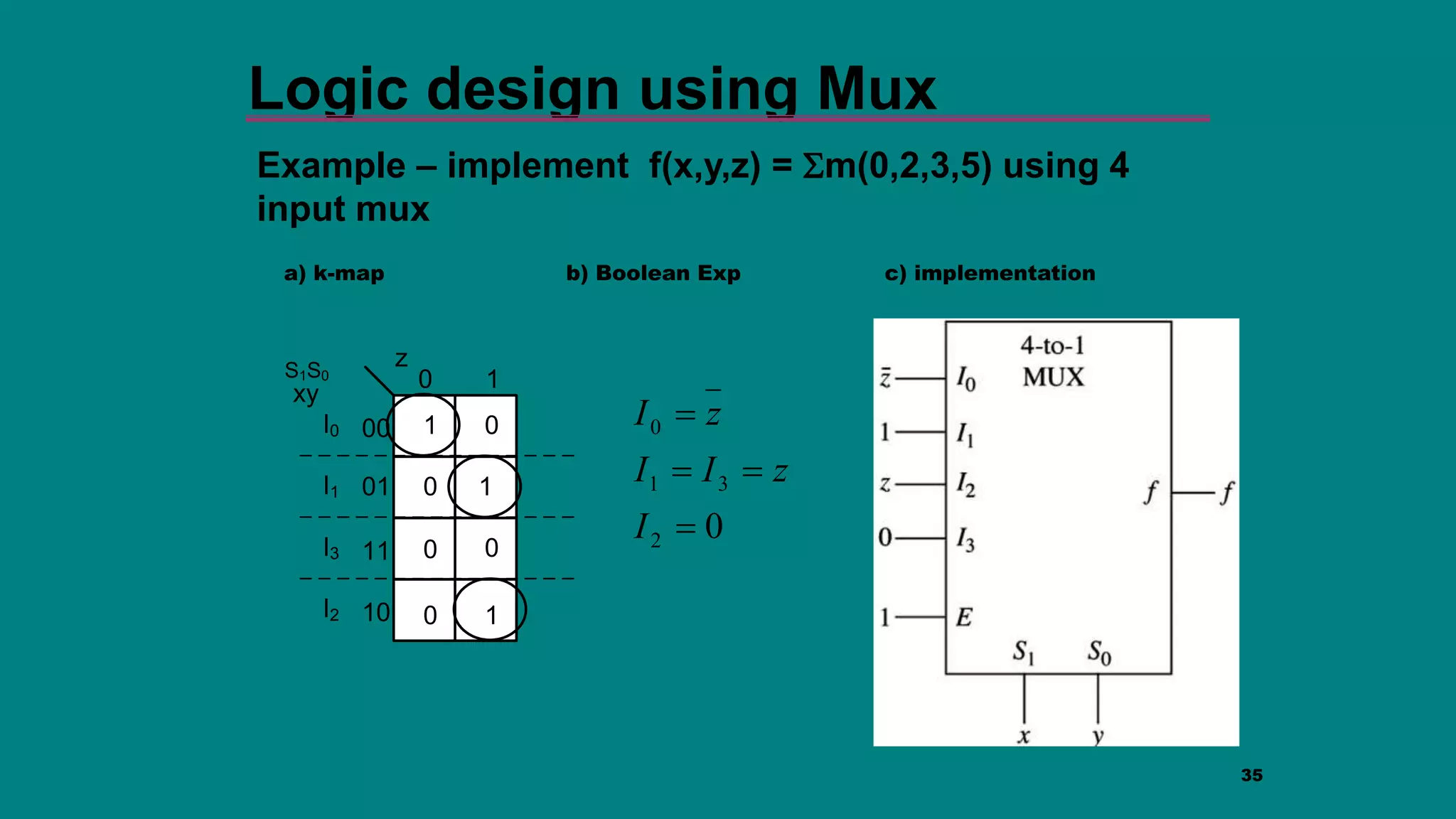
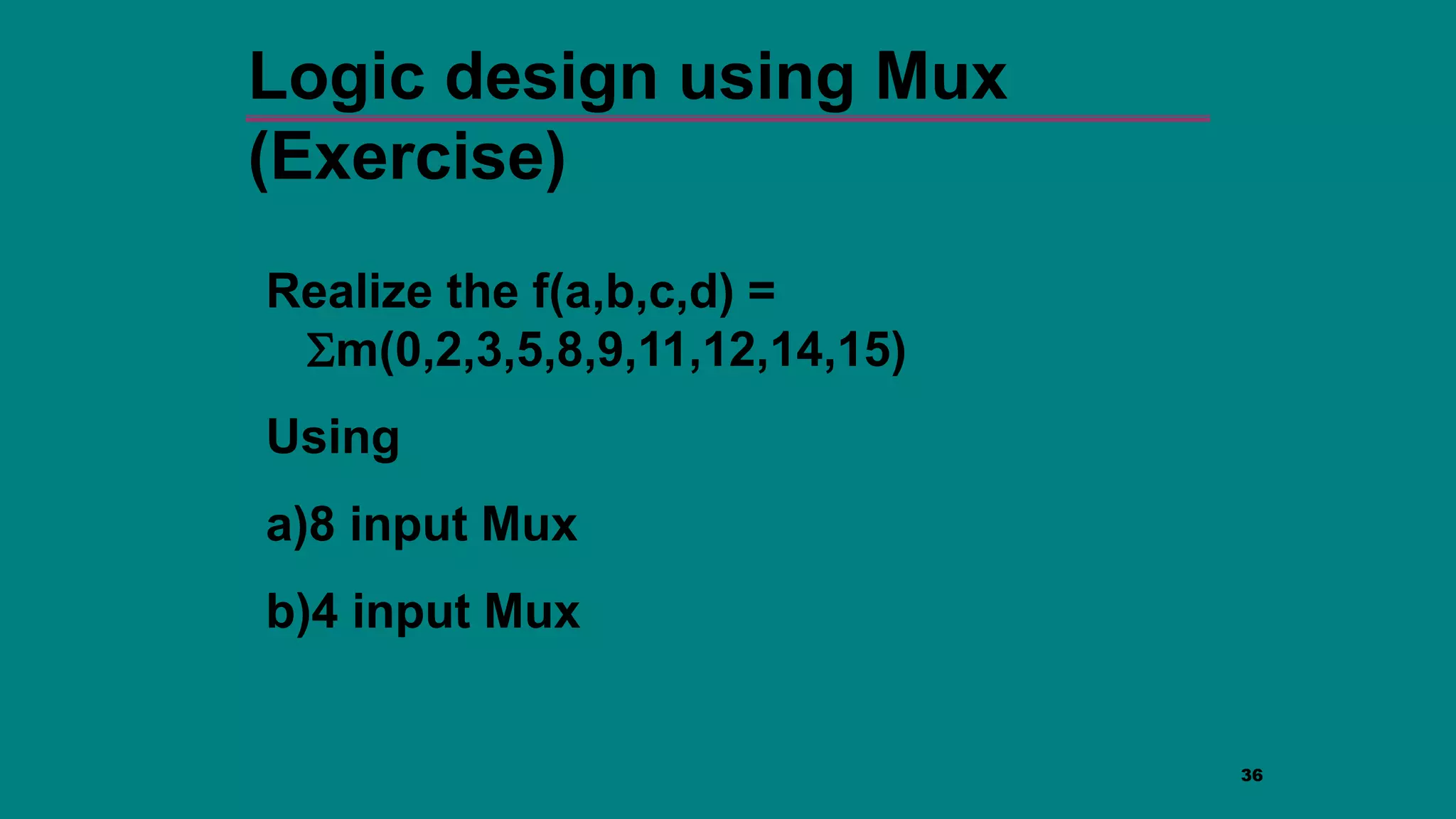
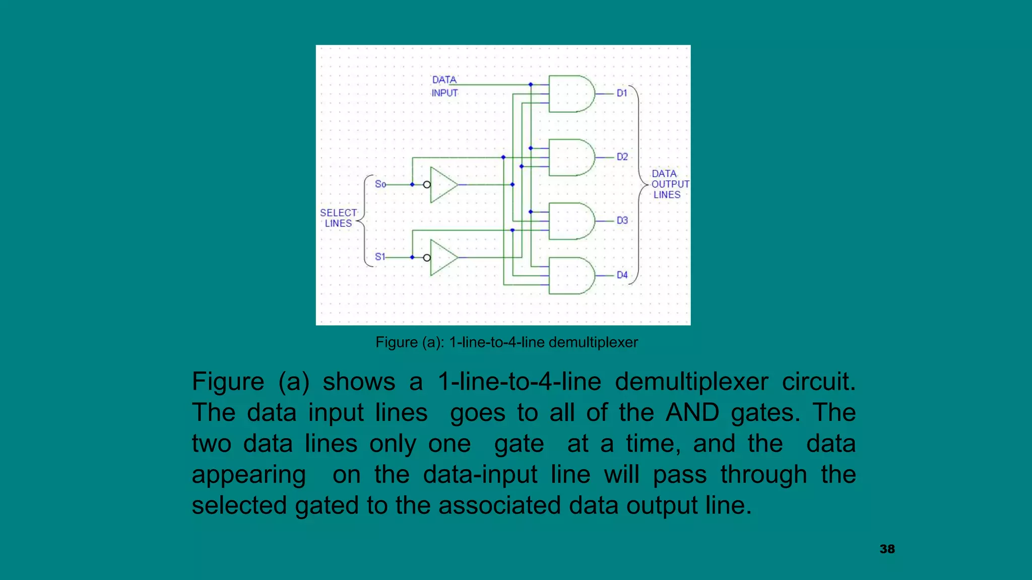
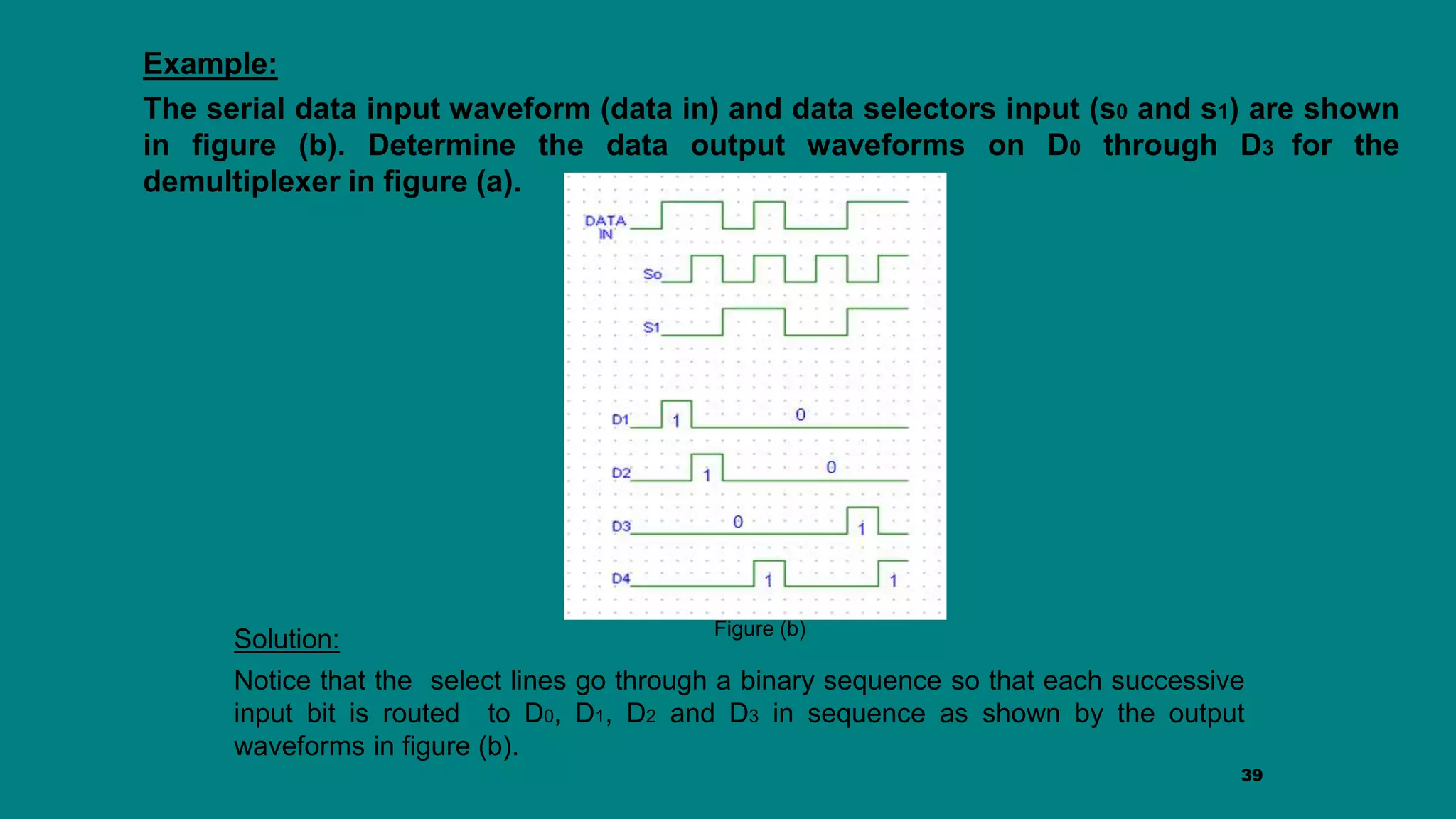
The document discusses combinational logic circuits including decoders, encoders, multiplexers and demultiplexers. It explains that decoders convert coded inputs to coded outputs, with only one output active at a time. Examples of 2-to-4 and 3-to-8 decoders are provided along with their truth tables and logic diagrams. Encoders perform the reverse function of decoders. Multiplexers allow selecting one of several data inputs to output, while demultiplexers distribute a single input to multiple outputs. Applications in designing logic functions using decoders and multiplexers are also covered.
This document discusses combinational circuit design and provides examples of various combinational logic circuits. It begins with an introduction that defines combinational and sequential circuits. The remainder of the document provides details on specific combinational logic circuits including half adders, full adders, subtractors, encoders, decoders, multiplexers, comparators, and code converters. Worked examples are provided for each circuit type using truth tables, Karnaugh maps, and logic diagrams. Applications of decoders for implementing functions like a full adder are also described.
The document discusses various topics related to combinational logic design including:
- The steps in the combinational logic design process including specification, formulation, optimization, technology mapping, and verification.
- Common functional blocks like decoders, encoders, multiplexers and their uses.
- Design of half adders, full adders, half subtractors, full subtractors and binary adders/subtractors.
- Implementation of logic functions using multiplexers and demultiplexers.
- Other topics like parity generators, code converters and hazards in combinational circuits.
This document discusses various digital logic components including encoders, decoders, multiplexers, and parity generators and checkers. It provides truth tables and logic diagrams for 8-to-3 encoders, 4-to-2 priority encoders, 2-to-4 decoders, 1-to-4 demultiplexers, even and odd parity generators, and even parity checkers. It also discusses implementing logic functions using multiplexers and decoders and gives examples of realizing functions with an 8x1 multiplexer. The document provides information on the basic operations of these components and their use in digital circuits.
This document discusses combinational logic design, specifically combinational logic functions and their implementation using decoders and multiplexers. It provides an overview of combinational logic and covers topics like rudimentary logic functions, decoding using decoders, encoding using encoders, and selecting using multiplexers. Examples are given for implementing combinational logic functions with decoders and multiplexers. Procedures for expanding decoders and multiplexers to handle more inputs and outputs are also described.
This document discusses various combinational and sequential logic blocks used in digital circuit design. It covers topics like adders, subtractors, multipliers, multiplexers, demultiplexers, decoders, encoders, flip-flops, registers, counters and finite state machines. It provides details on the design and working of different logic blocks like half adder, full adder, binary adder, magnitude comparator, encoder, decoder etc. with truth tables and logic diagrams. Examples are given to illustrate the implementation of logic functions using decoders and multiplexers.
The document describes decoders and encoders. It begins by explaining what a decoder is, providing examples of 2-to-4 and 3-to-8 decoders. It then discusses how decoders can be used to implement general logic and combinational circuits using decoders and OR gates. The document proceeds to describe specific decoder chips like the 74x139 and 74x138 decoders. It also discusses using 3-state buffers with decoders and building decoders from smaller decoders. The document then shifts to discussing encoders, 7-segment decoders, truth tables, and K-maps in the design of decoders and encoders. It concludes by discussing priority encoders and the 74x148 priority encoder chip.
The document provides instructions for a unit assignment involving simplification of logic expressions using the Variable Elimination Method (VEM) technique. It lists 3 steps - 1) simplify an expression using VEM, 2) obtain the minimal product, 3) simplify another expression using VEM. It then provides 4 logic expressions that need simplification.
4,encoder & decoder MUX and DEMUX EEng - Copy.pdfDamotTesfaye
This document discusses various combinational logic functions including decoding, encoding, multiplexing, and decoding. It provides details on decoder and encoder circuits. Decoders accept a binary input and activate only one output corresponding to that input. Encoders have multiple inputs but activate only one at a time, producing a binary output code. Examples of 3-line to 8-line decoders and 8-line to 3-line encoders are shown with their truth tables.
This chapter discusses methods for implementing combinational logic functions using circuits. It covers topics such as decoding, encoding, enabling functions, priority encoders, multiplexers, and implementing combinational functions using decoders and OR gates, multiplexers, ROMs, PLAs, PALs, and lookup tables. Implementation examples are provided for decoders, encoders, priority encoders, and multiplexers. The chapter also describes how to expand decoders and multiplexers to handle more inputs and outputs.
This chapter discusses combinational logic functions and circuits. It covers topics such as functions of single and multiple variables, decoding, encoding, selecting, and implementing combinational functions using decoders and OR gates, multiplexers, ROMs, PLAs, PALs, and lookup tables. Expansion techniques for decoders and multiplexers are also presented.
The document discusses combinational logic circuits. It describes combinational logic design procedures including specification, formulation, optimization, technology mapping, and verification. It also discusses analysis procedures for logic diagrams, including labeling gate outputs and determining Boolean functions. Additional topics covered include half adders, full adders, binary adders, decoders, encoders, multiplexers, priority encoders, and binary-coded decimal to seven-segment displays. Diagrams and truth tables are provided for various logic gates and circuits.
The document discusses common digital logic circuits including decoders, encoders, demultiplexers and multiplexers. It provides an overview of how these circuits work at a block level and then goes into more detail on decoders, describing their functionality, truth tables, and implementations including how to build larger decoders from smaller ones. Standard MSI decoder chips are also presented.
The document provides an overview of various data processing circuits including multiplexers, demultiplexers, decoders, encoders, adders, flip-flops and other logic gates. It describes the basic functionality and implementation of different types of multiplexers and demultiplexers with varying number of inputs and outputs. Decoder circuits like 1-of-16 decoder are explained along with their truth tables. Different arithmetic building blocks such as half adder, full adder and arithmetic logic unit are covered. The document also discusses flip-flops like RS, D, JK and their edge-triggered variations. Finally, it provides details on binary coded decimal representation.
DLD Lecture No 22 Decoder Circuit and Types of Decoder.pptxSaveraAyub2
This document discusses different types of decoders and their implementation. It begins by defining a decoder as a combinational circuit that converts binary input to a maximum of 2^n unique output lines, with only one output active at a time. It then discusses a 3-to-8 line decoder as an example, which decodes 3 inputs into 8 outputs, with each output representing one of the minterms. The document also covers implementing decoders with NAND gates, the four types of decoders based on enable and output polarity, and techniques for constructing larger decoders.
The truth table is not complete because it is missing the encoding for when no inputs are active. A complete truth table would include a row for all zero inputs to specify the output in that case.
The output equations are:
A0 = D7
A1 = D6 + D5 + D4 + D3
A2 = D2 + D1 + D0
This encodes the highest priority input on the lowest two bits, with the next two highest priorities on the middle bit, and any active input setting the highest bit.
1) The document describes the analysis and design procedures for combinational logic circuits. It discusses labeling gate outputs, determining boolean functions, and obtaining output functions through substitution.
2) An example 4-bit adder circuit is analyzed using these procedures to determine the boolean functions and truth table.
3) Implementation of half adders, full adders, binary adders, comparators, decoders, encoders, multiplexers and other common combinational logic circuits are described along with their boolean functions and truth tables. Verilog modeling of these circuits at gate level, dataflow level and behavioral level are also demonstrated.
Combination of circuit full ppt explainationhdhdjdkdjjdjdidididiisisiskkssjisshsuusushjwiwuueueuududhdndnd djdjdjje eurhebbe rudjenr r r earned d reuudbe d re eendbeuee ruebrbe r dudijsjsbd druirrndjidd didoosowkws eosooedknd eeiidkdididiidndndjd
Idjdjjdjjf fduudjdhdjjsb suejejen duejjebebb eiireiej nenndskaoaosowghdhdh
Jdjjddddddudjdjjsjaks shuddh djd d dudisiss sjaja dijdjdbddus
This document provides an overview of combinational logic circuits. It discusses the basic components and analysis procedures for combinational circuits. Examples are provided to demonstrate how to derive truth tables and Boolean functions from logic diagrams. Common combinational components like adders, decoders, encoders, and multiplexers are described along with their logic diagrams and implementations. HDL modeling techniques for combinational circuits using Verilog are also covered at the gate level and behavioral level.
The document discusses combinational logic circuits including decoders, encoders, multiplexers, demultiplexers, adders, subtractors, and magnitude comparators. It provides details on their design procedures, truth tables, logic diagrams, and implementations using basic logic gates. Combinational logic circuits have outputs that depend only on the current inputs and do not have memory elements.
combinational-circuit.pptx it tis creative study of digital electronics for ...RishabhSingh308993
This document discusses combinational logic circuits. It covers topics such as analysis procedures for logic diagrams, truth tables, Karnaugh maps, half adders, full adders, binary adders, subtractors, comparators, decoders, encoders, multiplexers, and HDL modeling of combinational circuits. Implementation examples are provided for various logic gates, adders, decoders, encoders, and multiplexers. Top-down and bottom-up design methodologies are also briefly discussed.
This document contains notes on combinational logic circuits including multiplexers, demultiplexers, encoders, and decoders. It provides circuit diagrams, truth tables, and explanations of the working principles for various digital components such as 2:1 and 4:1 multiplexers, 1:2 and 1:4 demultiplexers, priority encoders, decimal to BCD encoders, 3:8 decoders, and 2-bit comparators. Advantages of using multiplexers are also discussed, such as reducing the number of wires and circuit complexity.
Computer Organization And Architecture lab manualNitesh Dubey
The document discusses the implementation of various logic gates and flip-flops. It describes half adders and full adders can be implemented using XOR and AND gates. Binary to gray code and gray to binary code conversions are also explained. Circuit diagrams for 3-8 line decoder, 4x1 and 8x1 multiplexer are provided along with their truth tables. Finally, the working of common flip-flops like SR, JK, D and T are explained through their excitation tables.
Encoder, decoder, multiplexers and demultiplexerspubgalarab
This document discusses multiplexers, demultiplexers, encoders, and decoders. It provides examples and exercises for designing logic circuits using these components. Specifically, it describes how to use multiplexers and decoders to realize logic functions by mapping the minterms of the function to the inputs/outputs of the components. Exercises are included for designing an 8-to-1 multiplexer from 4-to-1 and 2-to-1 multiplexers, and designing a 4-to-16 decoder from 2-to-4 decoders. Priority encoders and decoders with enables are also covered.
A multiplexer is a digital circuit with multiple inputs and a single output. It selects one of the inputs using select lines and only allows one output at a time. A multiplexer can have 2, 4, 8, or more inputs depending on the number of select lines used. It is commonly used to route data within a computer from multiple sources to a single destination. Decoders are digital circuits that convert binary codes to activate a single output line. Common decoders include 2-to-4, 3-to-8, and 4-to-16 line decoders. Decoders are used whenever a specific combination of input levels needs to activate a single output. CMOS logic uses both n-type and p-type MOS
This document discusses combinational logic circuits. It begins with an outline of topics including Boolean algebra, decoders, encoders, and multiplexers. It then provides details on each of these topics. For decoders, it explains their function to decode an input value and provide an output. It provides truth tables for 2-to-4 and 3-to-8 decoders and shows how they can be constructed from logic gates. For encoders, it describes their inverse function of encoding inputs. Priority encoders and their truth tables are also covered. Finally, multiplexers are defined as using address bits to select a single input data line to output. Methods for constructing larger multiplexers from smaller ones are presented.
How to Build a Module in Odoo 17 Using the Scaffold MethodCeline George
Odoo provides an option for creating a module by using a single line command. By using this command the user can make a whole structure of a module. It is very easy for a beginner to make a module. There is no need to make each file manually. This slide will show how to create a module using the scaffold method.
Main Java[All of the Base Concepts}.docxadhitya5119
This is part 1 of my Java Learning Journey. This Contains Custom methods, classes, constructors, packages, multithreading , try- catch block, finally block and more.
More Related Content
Similar to ENG 202 – Digital Electronics 1 - Chapter 4 (1).pptx
This chapter discusses methods for implementing combinational logic functions using circuits. It covers topics such as decoding, encoding, enabling functions, priority encoders, multiplexers, and implementing combinational functions using decoders and OR gates, multiplexers, ROMs, PLAs, PALs, and lookup tables. Implementation examples are provided for decoders, encoders, priority encoders, and multiplexers. The chapter also describes how to expand decoders and multiplexers to handle more inputs and outputs.
This chapter discusses combinational logic functions and circuits. It covers topics such as functions of single and multiple variables, decoding, encoding, selecting, and implementing combinational functions using decoders and OR gates, multiplexers, ROMs, PLAs, PALs, and lookup tables. Expansion techniques for decoders and multiplexers are also presented.
The document discusses combinational logic circuits. It describes combinational logic design procedures including specification, formulation, optimization, technology mapping, and verification. It also discusses analysis procedures for logic diagrams, including labeling gate outputs and determining Boolean functions. Additional topics covered include half adders, full adders, binary adders, decoders, encoders, multiplexers, priority encoders, and binary-coded decimal to seven-segment displays. Diagrams and truth tables are provided for various logic gates and circuits.
The document discusses common digital logic circuits including decoders, encoders, demultiplexers and multiplexers. It provides an overview of how these circuits work at a block level and then goes into more detail on decoders, describing their functionality, truth tables, and implementations including how to build larger decoders from smaller ones. Standard MSI decoder chips are also presented.
The document provides an overview of various data processing circuits including multiplexers, demultiplexers, decoders, encoders, adders, flip-flops and other logic gates. It describes the basic functionality and implementation of different types of multiplexers and demultiplexers with varying number of inputs and outputs. Decoder circuits like 1-of-16 decoder are explained along with their truth tables. Different arithmetic building blocks such as half adder, full adder and arithmetic logic unit are covered. The document also discusses flip-flops like RS, D, JK and their edge-triggered variations. Finally, it provides details on binary coded decimal representation.
DLD Lecture No 22 Decoder Circuit and Types of Decoder.pptxSaveraAyub2
This document discusses different types of decoders and their implementation. It begins by defining a decoder as a combinational circuit that converts binary input to a maximum of 2^n unique output lines, with only one output active at a time. It then discusses a 3-to-8 line decoder as an example, which decodes 3 inputs into 8 outputs, with each output representing one of the minterms. The document also covers implementing decoders with NAND gates, the four types of decoders based on enable and output polarity, and techniques for constructing larger decoders.
The truth table is not complete because it is missing the encoding for when no inputs are active. A complete truth table would include a row for all zero inputs to specify the output in that case.
The output equations are:
A0 = D7
A1 = D6 + D5 + D4 + D3
A2 = D2 + D1 + D0
This encodes the highest priority input on the lowest two bits, with the next two highest priorities on the middle bit, and any active input setting the highest bit.
1) The document describes the analysis and design procedures for combinational logic circuits. It discusses labeling gate outputs, determining boolean functions, and obtaining output functions through substitution.
2) An example 4-bit adder circuit is analyzed using these procedures to determine the boolean functions and truth table.
3) Implementation of half adders, full adders, binary adders, comparators, decoders, encoders, multiplexers and other common combinational logic circuits are described along with their boolean functions and truth tables. Verilog modeling of these circuits at gate level, dataflow level and behavioral level are also demonstrated.
Combination of circuit full ppt explainationhdhdjdkdjjdjdidididiisisiskkssjisshsuusushjwiwuueueuududhdndnd djdjdjje eurhebbe rudjenr r r earned d reuudbe d re eendbeuee ruebrbe r dudijsjsbd druirrndjidd didoosowkws eosooedknd eeiidkdididiidndndjd
Idjdjjdjjf fduudjdhdjjsb suejejen duejjebebb eiireiej nenndskaoaosowghdhdh
Jdjjddddddudjdjjsjaks shuddh djd d dudisiss sjaja dijdjdbddus
This document provides an overview of combinational logic circuits. It discusses the basic components and analysis procedures for combinational circuits. Examples are provided to demonstrate how to derive truth tables and Boolean functions from logic diagrams. Common combinational components like adders, decoders, encoders, and multiplexers are described along with their logic diagrams and implementations. HDL modeling techniques for combinational circuits using Verilog are also covered at the gate level and behavioral level.
The document discusses combinational logic circuits including decoders, encoders, multiplexers, demultiplexers, adders, subtractors, and magnitude comparators. It provides details on their design procedures, truth tables, logic diagrams, and implementations using basic logic gates. Combinational logic circuits have outputs that depend only on the current inputs and do not have memory elements.
combinational-circuit.pptx it tis creative study of digital electronics for ...RishabhSingh308993
This document discusses combinational logic circuits. It covers topics such as analysis procedures for logic diagrams, truth tables, Karnaugh maps, half adders, full adders, binary adders, subtractors, comparators, decoders, encoders, multiplexers, and HDL modeling of combinational circuits. Implementation examples are provided for various logic gates, adders, decoders, encoders, and multiplexers. Top-down and bottom-up design methodologies are also briefly discussed.
This document contains notes on combinational logic circuits including multiplexers, demultiplexers, encoders, and decoders. It provides circuit diagrams, truth tables, and explanations of the working principles for various digital components such as 2:1 and 4:1 multiplexers, 1:2 and 1:4 demultiplexers, priority encoders, decimal to BCD encoders, 3:8 decoders, and 2-bit comparators. Advantages of using multiplexers are also discussed, such as reducing the number of wires and circuit complexity.
Computer Organization And Architecture lab manualNitesh Dubey
The document discusses the implementation of various logic gates and flip-flops. It describes half adders and full adders can be implemented using XOR and AND gates. Binary to gray code and gray to binary code conversions are also explained. Circuit diagrams for 3-8 line decoder, 4x1 and 8x1 multiplexer are provided along with their truth tables. Finally, the working of common flip-flops like SR, JK, D and T are explained through their excitation tables.
Encoder, decoder, multiplexers and demultiplexerspubgalarab
This document discusses multiplexers, demultiplexers, encoders, and decoders. It provides examples and exercises for designing logic circuits using these components. Specifically, it describes how to use multiplexers and decoders to realize logic functions by mapping the minterms of the function to the inputs/outputs of the components. Exercises are included for designing an 8-to-1 multiplexer from 4-to-1 and 2-to-1 multiplexers, and designing a 4-to-16 decoder from 2-to-4 decoders. Priority encoders and decoders with enables are also covered.
A multiplexer is a digital circuit with multiple inputs and a single output. It selects one of the inputs using select lines and only allows one output at a time. A multiplexer can have 2, 4, 8, or more inputs depending on the number of select lines used. It is commonly used to route data within a computer from multiple sources to a single destination. Decoders are digital circuits that convert binary codes to activate a single output line. Common decoders include 2-to-4, 3-to-8, and 4-to-16 line decoders. Decoders are used whenever a specific combination of input levels needs to activate a single output. CMOS logic uses both n-type and p-type MOS
This document discusses combinational logic circuits. It begins with an outline of topics including Boolean algebra, decoders, encoders, and multiplexers. It then provides details on each of these topics. For decoders, it explains their function to decode an input value and provide an output. It provides truth tables for 2-to-4 and 3-to-8 decoders and shows how they can be constructed from logic gates. For encoders, it describes their inverse function of encoding inputs. Priority encoders and their truth tables are also covered. Finally, multiplexers are defined as using address bits to select a single input data line to output. Methods for constructing larger multiplexers from smaller ones are presented.
Similar to ENG 202 – Digital Electronics 1 - Chapter 4 (1).pptx (20)
How to Build a Module in Odoo 17 Using the Scaffold MethodCeline George
Odoo provides an option for creating a module by using a single line command. By using this command the user can make a whole structure of a module. It is very easy for a beginner to make a module. There is no need to make each file manually. This slide will show how to create a module using the scaffold method.
Main Java[All of the Base Concepts}.docxadhitya5119
This is part 1 of my Java Learning Journey. This Contains Custom methods, classes, constructors, packages, multithreading , try- catch block, finally block and more.
Walmart Business+ and Spark Good for Nonprofits.pdfTechSoup
"Learn about all the ways Walmart supports nonprofit organizations.
You will hear from Liz Willett, the Head of Nonprofits, and hear about what Walmart is doing to help nonprofits, including Walmart Business and Spark Good. Walmart Business+ is a new offer for nonprofits that offers discounts and also streamlines nonprofits order and expense tracking, saving time and money.
The webinar may also give some examples on how nonprofits can best leverage Walmart Business+.
The event will cover the following::
Walmart Business + (https://business.walmart.com/plus) is a new shopping experience for nonprofits, schools, and local business customers that connects an exclusive online shopping experience to stores. Benefits include free delivery and shipping, a 'Spend Analytics” feature, special discounts, deals and tax-exempt shopping.
Special TechSoup offer for a free 180 days membership, and up to $150 in discounts on eligible orders.
Spark Good (walmart.com/sparkgood) is a charitable platform that enables nonprofits to receive donations directly from customers and associates.
Answers about how you can do more with Walmart!"
A review of the growth of the Israel Genealogy Research Association Database Collection for the last 12 months. Our collection is now passed the 3 million mark and still growing. See which archives have contributed the most. See the different types of records we have, and which years have had records added. You can also see what we have for the future.
it describes the bony anatomy including the femoral head , acetabulum, labrum . also discusses the capsule , ligaments . muscle that act on the hip joint and the range of motion are outlined. factors affecting hip joint stability and weight transmission through the joint are summarized.
How to Manage Your Lost Opportunities in Odoo 17 CRMCeline George
Odoo 17 CRM allows us to track why we lose sales opportunities with "Lost Reasons." This helps analyze our sales process and identify areas for improvement. Here's how to configure lost reasons in Odoo 17 CRM
हिंदी वर्णमाला पीपीटी, hindi alphabet PPT presentation, hindi varnamala PPT, Hindi Varnamala pdf, हिंदी स्वर, हिंदी व्यंजन, sikhiye hindi varnmala, dr. mulla adam ali, hindi language and literature, hindi alphabet with drawing, hindi alphabet pdf, hindi varnamala for childrens, hindi language, hindi varnamala practice for kids, https://www.drmullaadamali.com
Executive Directors Chat Leveraging AI for Diversity, Equity, and InclusionTechSoup
Let’s explore the intersection of technology and equity in the final session of our DEI series. Discover how AI tools, like ChatGPT, can be used to support and enhance your nonprofit's DEI initiatives. Participants will gain insights into practical AI applications and get tips for leveraging technology to advance their DEI goals.
What is Digital Literacy? A guest blog from Andy McLaughlin, University of Ab...
ENG 202 – Digital Electronics 1 - Chapter 4 (1).pptx
1. ENG 202 – Digital
Electronics 1
CHAPTER 4 – Combinational Logic Circuit
2. 2
Course Learning Outcomes, CLO
CLO 4:
explain correctly the application of
data processing circuits in digital
systems.
3. SUMMARY
School of Electrical Engineering 3
DATA PROCESSING CIRCUITS
Encoder,
Decoder,
BCD to Seven Segment Display
Decoder,
Multiplexer
Demultiplexer.
4. Decoder
• Decoder: a multiple input, multiple output logic circuit which converts
coded input into coded output from n input line to a maximum of 2n
unique output lines.
• activates an output that corresponds to a binary number on the input.
• Only one output is active for any given input
4
5. Decoder
• The basic function is to detect the presence of a specified
combination of bits (code) on its inputs and to indicate the
presence of that code by a specified output level
• In other word, decoder circuit look at its inputs, determine
which binary number present there, and activates the
output that correspond to that numbers; all other outputs
remain inactive
• Some decoder do not utilize the 2n possible input codes for
example BCD to decimal decoder and Seven segment
decoder
5
6. 2-to-4 Decoder (Active HIGH)
6
2-to-4
Decoder
A
B
O0
O1
O2
O3
b) Truth table
a) Logic symbol
O0 = A’B’
O1 = A’B
O2 = AB’
O3 = AB
c) Boolean expression
O0
O1
O2
O3
A B
d) Logic diagram
@
7. 2-to-4 Decoder (Active LOW)
2 to 4
Decoder
21
20
O0
O1
O2
O3
A
B
2 to 4
Decoder
21
20
O0
O1
O2
O3
A
B
O0
O1
O2
O3
A B
O0
O1
O2
O3
A B
7
a) Logic symbol
@
b) Truth table c) Boolean expression
AB
O
B
A
O
B
A
O
B
A
O
3
2
1
0
d) Logic diagram
8. 2-to-4 Decoder with active LOW enable input
8
AB
en
D
B
A
en
D
B
A
en
D
B
A
en
D
3
1
2
0
,
,
a) Logic symbol b) Truth table
c) Boolean expression
d) Logic diagram
Enable input used to control the
operation of the decoderActive
mode is ‘0’- active low
9. The 74x139 Dual 2-to-4 Decoder
9
a) Logic symbol
b) Logic diagram
1 1 1 1
1 1 1 0
1 1 0 1
1 0 1 1
0 1 1 1
1 X X
0 0 0
0 0 1
0 1 0
0 1 1
Y3 Y2 Y1 Y0
G B A
Outputs
Inputs
Truth table for one-half of a
74x139 dual 2-to-4 decoder
10. 10
3 to 8 Binary Decoder (active HIGH)
3-to-8
Decoder
X
Y
F0
F1
F2
F3
F4
F5
F6
F7
Z
a) Logic symbol
x y z F0 F1 F2 F3 F4 F5 F6 F7
0 0 0 1 0 0 0 0 0 0 0
0 0 1 0 1 0 0 0 0 0 0
0 1 0 0 0 1 0 0 0 0 0
0 1 1 0 0 0 1 0 0 0 0
1 0 0 0 0 0 0 1 0 0 0
1 0 1 0 0 0 0 0 1 0 0
1 1 0 0 0 0 0 0 0 1 0
1 1 1 0 0 0 0 0 0 0 1
F1 = x'y'z
x z
y
F0 = x'y'z'
F2 = x'yz'
F3 = x'yz
F5 = xy'z
F4 = xy'z'
F6 = xyz'
F7 = xyz
b) Truth table
c) Logic diagram & Boolean Expression
13. 13
The equation for the output signal Y5:
Active-low
It has three enable inputs, G1, G2A, G2B , all of which
must be asserted for the selected output to be asserted.
The 74x138 3-to-8 Decoder
A
B
C
B
G
A
G
G
Y 2
2
1
5
14. Exercise
• Design a decoder listing below
a) BCD to decimal decoder
b) 4 to 16 decoder
14
15. Seven Segment Display
• Used for displaying information in a form that can be
understood by user or operator.
• Information can be in alphanumeric (numbers and
letters).
• Seven segment configuration which its arrangement
uses LED for each segment.
• two ways of arrangement – common anode and
common cathode.
• Each arrangement needs different driver/ decoder to
drive each segment of seven segment display.
15
17. A B C D a b c d e f g
0 0 0 0
0 0 0 1
0 0 1 0
0 0 1 1
0 1 0 0
0 1 0 1
0 1 1 0
0 1 1 1
1 0 0 0
1 0 0 1
1 0 1 0
1 0 1 1
1 1 0 0
1 1 0 1
1 1 1 0
1 1 1 1
17
FILL IN THE TRUTH FOR ACTIVE LOW BCD TO 7 SEGMENT DECODER
18. • Any combinational circuit with n inputs and m outputs can
be implemented with an n-to-2n decoder (active HIGH)
with m OR gates to generate a minterms
OR gate forms the sum
The output lines of the decoder corresponding to the
minterms of the function are used as inputs to the or
gate
• Suitable when a circuit has many outputs, and each
output function is expressed with few minterms.
• It can also use AND gates and n-to-2n decoder to generate
a Maxterm function.
18
Decoder applications
19. • Example: Full adder
• S(x, y, z) = S (1,2,4,7)
• C(x, y, z) = S (3,5,6,7)
19
Decoder applications (full adder)
x y z C S
0 0 0 0 0
0 0 1 0 1
0 1 0 0 1
0 1 1 1 0
1 0 0 0 1
1 0 1 1 0
1 1 0 1 0
1 1 1 1 1
3-to-8
Decoder
S2
S1
S0
x
y
z
0
1
2
3
4
5
6
7
S
C
a) Truth table b) Minterm Expression
21. 21
f1(x2,x1,x0) = Sm(0,2,6,7) and f2(x2,x1,x0) = Sm(3,5,6,7)
(a) Using output and-gates. (b) Using output nand-gates.
Application Example
Decoder applications example
22. • An encoder is a combinational logic circuit that essentially
performs a ‘reverse’ of decoder function
• Number of input lines is larger than output lines
• Decoder VS Encoder
22
Encoder
Decoder Encoder
23. • Only one of input lines is activated at a given time and
produces an N-bit output code depending on which input is
active.
• For example octal to binary encoder: if input 4 is active, the
output code should be 100 with 1 is MSB bit.
23
Encoder
26. Decimal to BCD Priority Encoder
26
The priority function means that the encoder will produce
a BCD output corresponding to the highest-order decimal
digit input that is active and will ignore any other actives
input
27. Multiplexer
• A multiplexer is a device that allows digitals information
from several sources to be routed onto a single line for
transmission over that line to a common destination
• The basic multiplexer has several data-input line and a single
output line
• has data select inputs, which permit digital data on any one
of the inputs to be switched to the output line
• also known as data selector
27
29. 2 - to - 1 Multiplexer
2 input
Mux
I0
I1
z
s
29
b) Truth Table
c) Boolean Expression
d) Logic Circuit
a) Logic Symbol
30. 4 - to - 1 Multiplexer
4 input
Mux
z
S1
I0
I3
I2
I1
S0
30
c) Boolean Expression
b) Truth Table
a) Logic Symbol d) Logic diagram
3
0
1
2
0
1
1
0
1
0
0
1 I
S
S
I
S
S
I
S
S
I
S
S
z
33. Logic design using Mux
• Case1- number of input is equal to
number of select lines
• Design procedure
• Connect inputs to selected
lines
• Identify the decimal number
corresponding to each
minterm in the expression
• Connect logic 1 level to input
lines corresponding to these
numbers
• Connect logic 0 level to the
others
33
f(x,y,z) = Sm(0,2,3,5)
Example - 3 variable function using 8-to1 line Multiplexer
34. 34
Logic design using Mux
Case 2: Number of inputs is
higher than number of select
lines
Design procedure
Reduce the number of inputs to
the number of select lines by
inspection
k-map
36. 36
Logic design using Mux
(Exercise)
Realize the f(a,b,c,d) =
Sm(0,2,3,5,8,9,11,12,14,15)
Using
a)8 input Mux
b)4 input Mux
37. 37
Demultiplexer (Demux)
Basically reverses the multiplexing function
Takes data from one line and distributes them
to a given numbers of output lines.
Demultiplexer also known as a data distributor.
Decoders can also be used as a
demultiplexers.
38. 38
Figure (a) shows a 1-line-to-4-line demultiplexer circuit.
The data input lines goes to all of the AND gates. The
two data lines only one gate at a time, and the data
appearing on the data-input line will pass through the
selected gated to the associated data output line.
Figure (a): 1-line-to-4-line demultiplexer
39. 39
Example:
The serial data input waveform (data in) and data selectors input (s0 and s1) are shown
in figure (b). Determine the data output waveforms on D0 through D3 for the
demultiplexer in figure (a).
Solution:
Notice that the select lines go through a binary sequence so that each successive
input bit is routed to D0, D1, D2 and D3 in sequence as shown by the output
waveforms in figure (b).
Figure (b)