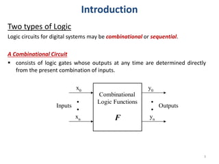
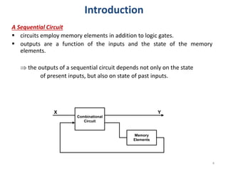
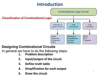
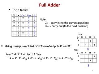
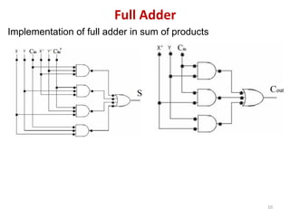
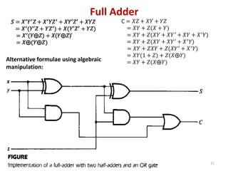
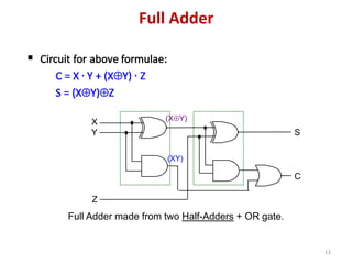
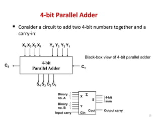
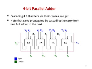
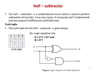
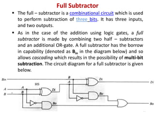
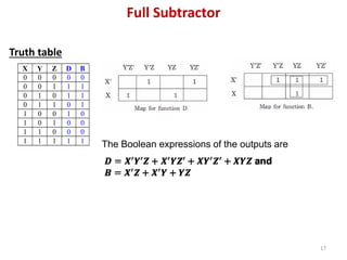
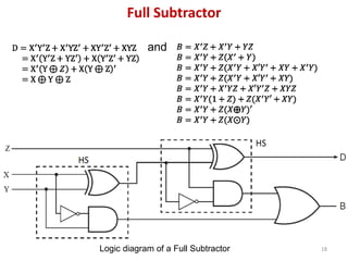
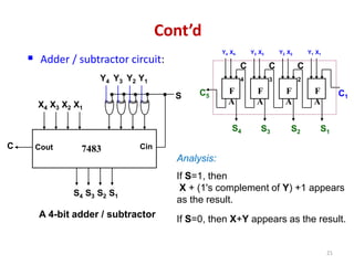
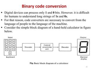
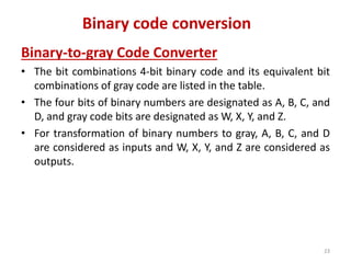
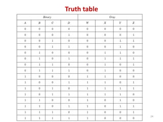
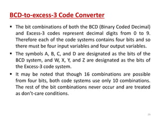
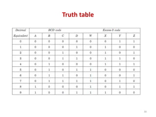
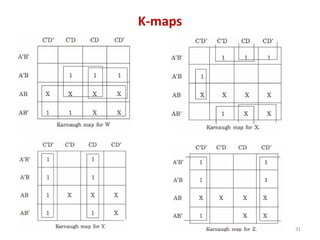
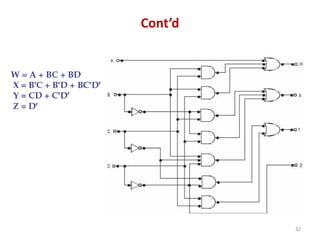
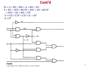
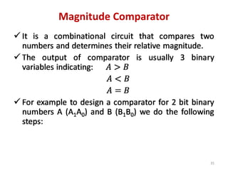
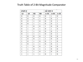
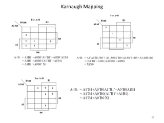
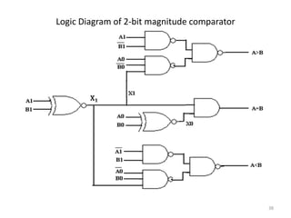
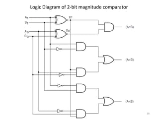
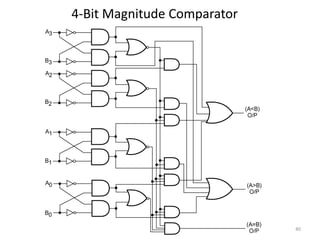
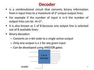
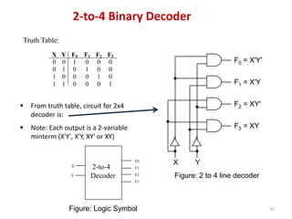
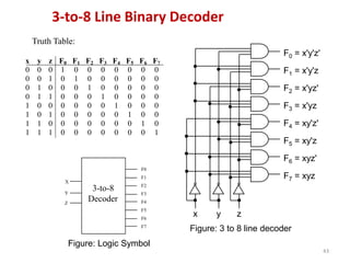
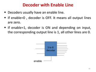
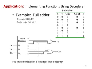
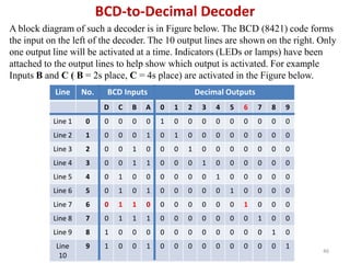
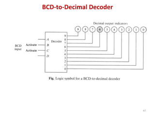
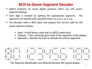
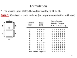
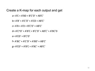
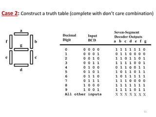
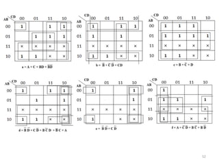
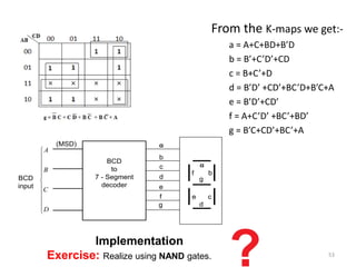
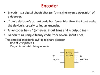
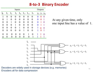
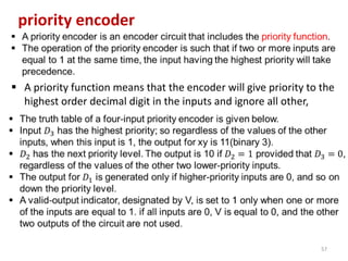
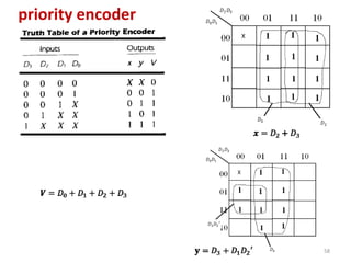
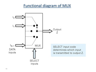
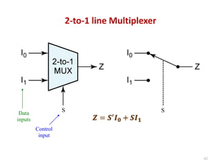
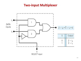
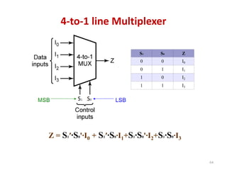
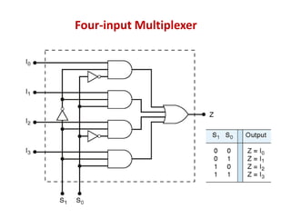
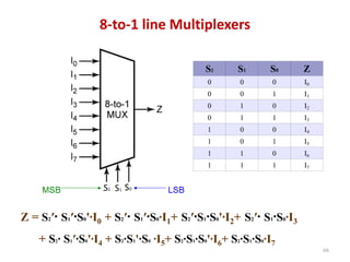
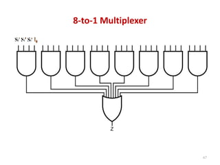
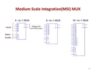
Chapter 4
Combinational circuit design
1
Chapter outline
 Introduction
 Adders
 Subtractors
 Binary code conversion
 Magnitude comparator
 Parity generator and checker
 Decoders
 Encoders
 Multiplexers
 Multiplexer tree
2
 Demultiplexers
 Demultiplexer tree
 Combinational Logic with MSI
and LSI
 Combinational logic design using
multiplexers
 Demultiplexers/Decoders and
their use in combinational logic
design
Introduction
Two types of Logic
Logic circuits for digital systems may be combinational or sequential.
A Combinational Circuit
 consists of logic gates whose outputs at any time are determined directly
from the present combination of inputs.
x0
xn
y0
yn
Inputs Outputs
.
.
.
.
Combinational
Logic Functions
F
3
A Sequential Circuit
 circuits employ memory elements in addition to logic gates.
 outputs are a function of the inputs and the state of the memory
elements.
 the outputs of a sequential circuit depends not only on the state
of present inputs, but also on state of past inputs.
Combinational
Circuit
Memory
Elements
X Y
4
Introduction
5
Introduction
1. Problem description
2. Input/output of the circuit
3. Define truth table
4. Simplification for each output
5. Draw the circuit
In general we have to do the following steps:
Designing Combinational Circuits
Classification of Combinational Logic
6
Half Adder
 Half Adder Is a circuit which adds two single bits (say X,Y) together, to
produce a result of two bits (called C, S).
 Design procedure:
1) State Problem
Example: Build a Half Adder to add two bits
2) Determine and label the inputs & outputs of circuit.
Example: Two inputs and two outputs labeled, as follows:
Half
Adder
X
Y
S
C
(X + Y)
3) Draw truth table:
X Y C S
0 0 0 0
0 1 0 1
1 0 0 1
1 1 1 0
7
X Y C S
0 0 0 0
0 1 0 1
1 0 0 1
1 1 1 0
X
Y
S
C
Half Adder
5) Draw logic diagram.
y
0
1
0 1
0
1
x
0
0
y
0
1
0 1
0
0
x
1
1
Half Adder
C S
8
Full Adder
 Half-adder adds up only two bits.
 To add two binary numbers, we need to add 3 bits (including the carry).
 Example:
1 1 1 carry
0 0 1 1 X
+ 0 1 1 1 Y
1 0 1 0 S
 Need Full Adder (so called as it can be made from two half-adders).
Full
Adder
X
Y
Cin
S
Cout
(X + Y + Cin)
9
 Truth table:
X Y Cin Cout S
0 0 0 0 0
0 0 1 0 1
0 1 0 0 1
0 1 1 1 0
1 0 0 0 1
1 0 1 1 0
1 1 0 1 0
1 1 1 1 1
Note:
Cin - carry in (to the current position)
Cout - carry out (to the next position)
0
1
00 01 11 10
X
YCin
1
1
1
1
C
0
1
00 01 11 10
X
1
1
1
1
S
Full Adder
YCin
10
Implementation of full adder in sum of products
Full Adder
11
Full Adder
Alternative formulae using algebraic
manipulation:
12
Full Adder made from two Half-Adders + OR gate.
(XY)
X
Y S
C
Z
(XY)
Full Adder
13
4-bit Parallel Adder
 Consider a circuit to add two 4-bit numbers together and a
carry-in:
4-bit
Parallel Adder
C5 C1
X2 X1 Y4 Y3
S4 S3 S2 S1
Y2 Y1
X4 X3
Black-box view of 4-bit parallel adder
X
Y
S
Cout
S
Cin
Input carry
Binary
no. B
Binary
no. A
Output carry
4-bit
sum
14
 Cascading 4 full adders via their carries, we get:
 Note that carry propagated by cascading the carry from
one full adder to the next.
C1
Y1 X1
S1
FA
C2
C5
Y2 X2
S2
FA
C3
Y3 X3
S3
FA
C4
Y4 X4
S4
FA
Output
Input
4-bit Parallel Adder
Half – subtractor
 The half – subtractor is a combinational circuit which is used to perform
subtraction of two bits. It has two inputs, X (minuend) and Y (subtrahend)
and two outputs D (difference) and B (borrow).
Truth table
 The truth table for the half – subtractor is given below.
15
X Y D B
0 0 0 0
0 1 1 1
1 0 1 0
1 1 0 0
So, Logic equations are:
D = X’Y + XY’ and
B = X’Y
truth table
Full Subtractor
 The full – subtractor is a combinational circuit which is used
to perform subtraction of three bits. It has three inputs,
and two outputs.
 As in the case of the addition using logic gates, a full
subtractor is made by combining two half – subtractors
and an additional OR-gate. A full subtractor has the borrow
in capability (denoted as Bin in the diagram below) and so
allows cascading which results in the possibility of multi-bit
subtraction. The circuit diagram for a full subtractor is given
below.
16
Truth table
17
X Y Z D B
0 0 0 0 0
0 0 1 1 1
0 1 0 1 1
0 1 1 0 1
1 0 0 1 0
1 0 1 0 0
1 1 0 0 0
1 1 1 1 1
The Boolean expressions of the outputs are
Full Subtractor
18
Logic diagram of a Full Subtractor
and
Full Subtractor
19
Addition/Subtraction in 2’s complement
Representation
Recall that:
X-Y = X + (-Y)
= X + (2’s complement of Y)
= X + (1’s complement of Y) +1
X+Y = X + (Y)
20
Cont’d
 Design requires:
(i) XOR gates:
such that: output = Y when S = 0
= Y' when S = 1
(ii) S connected to carry-in.
S = 0
Y
Y
S = 1
Y'
Y
21
Cont’d
 Adder / subtractor circuit:
Analysis:
If S=1, then
X + (1's complement of Y) +1 appears
as the result.
If S=0, then X+Y appears as the result.
7483
X2 X1
Y4 Y3 Y2 Y1
X4 X3
S2 S1
S4 S3
C
S
Cin
Cout
A 4-bit adder / subtractor
C1
Y1 X1
S1
F
A
C
2
C5
Y2 X2
S2
F
A
C
3
Y3 X3
S3
F
A
C
4
Y4 X4
S4
F
A
Binary code conversion
22
 Digital devices can process only 1 and 0 bits. However. it is difficult
for humans to understand long strings of 1s and 0s.
 For that reason, code converters arc necessary to convert from the
language of people to the language of the machine.
 Consider the simple block diagram of a hand-held calculator in figure
below.
Binary-to-gray Code Converter
• The bit combinations 4-bit binary code and its equivalent bit
combinations of gray code are listed in the table.
• The four bits of binary numbers are designated as A, B, C, and
D, and gray code bits are designated as W, X, Y, and Z.
• For transformation of binary numbers to gray, A, B, C, and D
are considered as inputs and W, X, Y, and Z are considered as
outputs.
23
Binary code conversion
Truth table
24
K-maps
25
Logic equation & logic diagram of a
binary to gray code convertor
26
Gray-to-binary code convertor
27
28
BCD-to-excess-3 Code Converter
29
 The bit combinations of both the BCD (Binary Coded Decimal)
and Excess-3 codes represent decimal digits from 0 to 9.
Therefore each of the code systems contains four bits and so
there must be four input variables and four output variables.
 The symbols A, B, C, and D are designated as the bits of the
BCD system, and W, X, Y, and Z are designated as the bits of
the Excess-3 code system.
 It may be noted that though 16 combinations are possible
from four bits, both code systems use only 10 combinations.
The rest of the bit combinations never occur and are treated
as don’t-care conditions.
Truth table
30
K-maps
31
Cont’d
32
33
Cont’d
Excess-3 - to – BCD Code Converter
 Assignment
34
Magnitude Comparator
35
Truth Table of 2-Bit Magnitude Comparator
36
Karnaugh Mapping
37
Logic Diagram of 2-bit magnitude comparator
38
39
Logic Diagram of 2-bit magnitude comparator
4-Bit Magnitude Comparator
40
Decoder
 Is a combinational circuit that converts binary information
from n input lines to a maximum of 2n unique output lines.
 For example if the number of input is n=3 the number of
output lines can be m=23 .
 It is also known as 1 of 8 because one output line is selected
out of 8 available lines:
 Binary decoders
– Converts an n-bit code to a single active output
– Only one output is a 1 for any given input
– Can be developed using AND/OR gates
3 to 8
decoder
enable 41
2-to-4 Binary Decoder
 From truth table, circuit for 2x4
decoder is:
 Note: Each output is a 2-variable
minterm (X'Y', X'Y, XY' or XY)
X Y F0 F1 F2 F3
0 0 1 0 0 0
0 1 0 1 0 0
1 0 0 0 1 0
1 1 0 0 0 1
F0 = X'Y'
F1 = X'Y
F2 = XY'
F3 = XY
X Y
Truth Table:
2-to-4
Decoder
X
Y
F0
F1
F2
F3
42
Figure: 2 to 4 line decoder
Figure: Logic Symbol
3-to-8 Line Binary Decoder
x y z F0 F1 F2 F3 F4 F5 F6 F7
0 0 0 1 0 0 0 0 0 0 0
0 0 1 0 1 0 0 0 0 0 0
0 1 0 0 0 1 0 0 0 0 0
0 1 1 0 0 0 1 0 0 0 0
1 0 0 0 0 0 0 1 0 0 0
1 0 1 0 0 0 0 0 1 0 0
1 1 0 0 0 0 0 0 0 1 0
1 1 1 0 0 0 0 0 0 0 1
F1 = x'y'z
x z
y
F0 = x'y'z'
F2 = x'yz'
F3 = x'yz
F5 = xy'z
F4 = xy'z'
F6 = xyz'
F7 = xyz
Truth Table:
3-to-8
Decoder
X
Y
F0
F1
F2
F3
F4
F5
F6
F7
Z
43
Figure: 3 to 8 line decoder
Figure: Logic Symbol
Decoder with Enable Line
 Decoders usually have an enable line.
 If enable=0 , decoder is OFF. It means all output lines
are zero.
 If enable=1, decoder is ON and depending on input,
the corresponding output line is 1, all other lines are 0.
44
3 to 8
decoder
enable
Application: Implementing Functions Using Decoders
• Example: Full adder
S(x, y, z) = S (1,2,4,7)
Cout(x, y, z) = S (3,5,6,7)
3-to-8
Decoder
S2
S1
S0
x
y
Cin
0
1
2
3
4
5
6
7
S
Cout
x y Cin Cout S
0 0 0 0 0
0 0 1 0 1
0 1 0 0 1
0 1 1 1 0
1 0 0 0 1
1 0 1 1 0
1 1 0 1 0
1 1 1 1 1
45
Fig. Implementation of a full adder with a decoder
truth table
46
BCD-to-Decimal Decoder
A block diagram of such a decoder is in Figure below. The BCD (8421) code forms
the input on the left of the decoder. The 10 output lines are shown on the right. Only
one output line will be activated at a time. Indicators (LEDs or lamps) have been
attached to the output lines to help show which output is activated. For example
Inputs B and C ( B = 2s place, C = 4s place) are activated in the Figure below.
Line No. BCD Inputs Decimal Outputs
D C B A 0 1 2 3 4 5 6 7 8 9
Line 1 0 0 0 0 0 1 0 0 0 0 0 0 0 0 0
Line 2 1 0 0 0 1 0 1 0 0 0 0 0 0 0 0
Line 3 2 0 0 1 0 0 0 1 0 0 0 0 0 0 0
Line 4 3 0 0 1 1 0 0 0 1 0 0 0 0 0 0
Line 5 4 0 1 0 0 0 0 0 0 1 0 0 0 0 0
Line 6 5 0 1 0 1 0 0 0 0 0 1 0 0 0 0
Line 7 6 0 1 1 0 0 0 0 0 0 0 1 0 0 0
Line 8 7 0 1 1 1 0 0 0 0 0 0 0 1 0 0
Line 9 8 1 0 0 0 0 0 0 0 0 0 0 0 1 0
Line
10
9 1 0 0 1 0 0 0 0 0 0 0 0 0 1
47
BCD-to-Decimal Decoder
BCD-to-Seven-Segment Decoder
 Digital readouts on many digital products often use LED seven-
segment displays.
 Each digit is created by lighting the appropriate segments. The
segments are labeled with standard letters as a, b, c, d, e, f, g.
 The decoder takes a BCD input and outputs the correct code for the
seven-segment display.
48
 Input: A 4-bit binary value that is a BCD coded input.
 Outputs: 7 bits, a through g for each of the segments of the display.
 Operation: Decode the input to activate the correct segments.
Fig. Segment Identification and Decimal Number with typical display
a
b
f
c
d
e
g
Formulation
 For unused input states, the output is either a ‘0’ or ‘X’.
Case 1: Construct a truth table for (Incomplete combination with zero)
49
50
a= A’C + A’BD + B’C’D’ + AB’C’
b= A’B’ + A’C’D’ + A’CD + AB’C’
c= A’B + A’D + B’C’D’ + AB’C’
d= A’C^D’ + A’B’C + B’C’D’ + AB’C’ + A’BC’D
e= A’CD’ + B’C’D’
f= A’BC’ + A’C’D’ + A’BD’ + AB’C’
g= A’CD’ + A’B’C + A’BC’ + AB’C’
Create a K-map for each output and get
51
Case 2: Construct a truth table (complete with don’t care combination)
52
53
From the K-maps we get:-
a = A+C+BD+B’D
b = B’+C’D’+CD
c = B+C’+D
d = B’D’ +CD’+BC’D+B’C+A
e = B’D’+CD’
f = A+C’D’ +BC’+BD’
g = B’C+CD’+BC’+A
BCD
to
7 - Segment
decoder
a
b
f
c
d
e
g
a
b
c
d
e
f
g











D
C
B
A
BCD
input
(MSD)
Implementation
Exercise: Realize using NAND gates.
Encoder
54
.
.
.
.
.
.
2n
inputs
n
outputs
Binary
encoder
The simplest encoder is a 2n-to-n binary encoder
One of 2n inputs = 1
Output is an n-bit binary number
8-to-3 Binary Encoder
At any given time, only
one input line has a value of 1.
Inputs Outputs
I0 I1 I2 I3 I4 I 5 I 6 I7 y2 y1 y0
1 0 0 0 0 0 0 0 0 0 0
0 1 0 0 0 0 0 0 0 0 1
0 0 1 0 0 0 0 0 0 1 0
0 0 0 1 0 0 0 0 0 1 1
0 0 0 0 1 0 0 0 1 0 0
0 0 0 0 0 1 0 0 1 0 1
0 0 0 0 0 0 1 0 1 1 0
0 0 0 0 0 0 0 1 1 1 1
I0
I1
I2
I3
I4
I5
I6
I7
y0 = I1 + I3 + I5 + I7
y1 = I2 + I3 + I6 + I7
y2 = I4 + I5 + I6 + I7
55
Decoders are widely used in storage devices (e.g. memories)
Encoders all for data compression
Limitations of 8 to 3 encoder
1. If two inputs are active simultaneously, the output produces an
undefined combination. For example, if I3 and I6 are 1
simultaneously, the output of the encoder will be 111 because all
three o/ps are equal to 1. this does not represent binary 3 nor
binary 6. To resolve this ambiguity, encoder circuits must
establish a priority to ensure that only one input is encoded.
2. Another ambiguity in octal to binary encoder is that an o/p with
0’s is generated when all the inputs are 0. The problem is that an
o/p with all 0’s is also generated when I0 is equal to 1. This
ambiguity can be resolved by providing an additional o/p that
specifies the condition that none of the inputs are active.
56
priority encoder
57
 A priority function means that the encoder will give priority to the
highest order decimal digit in the inputs and ignore all other,
58
priority encoder
59
According to the above Boolean expression, the priory encoder is implemented as:
Exercise: design a decimal to BCD priority encoder.
Multiplexer
 Multiplexing means transmitting a large number of information
units over a smaller number of channels or lines.
 Multiplexer (MUX) is a combinational circuit that selects binary
information from one of the input lines and directs it to a single
output line
 Usually there are 2n input lines and n selection lines whose bit
combinations determine which input line is selected
 Multiplexers also known as Data Selectors
 For example for 2-to-1 multiplexer if selection S is zero then I0 has
the path to output and if S is one I1 has the path to output.
 Multiplexers are used in any application in which data must be
switched from multiple sources to a destination.
e.g., processor’s registers to ALU
60
61
Functional diagram of MUX
62
2-to-1 line Multiplexer
Data
inputs
Control
input
63
Two-input Multiplexer
64
4-to-1 line Multiplexer
Z = S1′∙S0'∙I0 + S1′∙S0∙I1+S1∙S0'∙I2+S1∙S0∙I3
S1 S0 Z
0 0 I0
0 1 I1
1 0 I2
1 1 I3
65
Four-input Multiplexer
66
8-to-1 line Multiplexers
S2 S1 S0 Z
0 0 0 I0
0 0 1 I1
0 1 0 I2
0 1 1 I3
1 0 0 I4
1 0 1 I5
1 1 0 I6
1 1 1 I7
Z = S2′∙ S1′∙S0'∙I0 + S2′∙ S1′∙S0∙I1+ S2′∙S1∙S0'∙I2+ S2′∙ S1∙S0∙I3
+ S2∙ S1′∙S0'∙I4 + S2∙S1'∙S0 ∙I5+ S2∙S1∙S0'∙I6+ S2∙S1∙S0∙I7
67
8-to-1 Multiplexer
Medium Scale Integration(MSI) MUX
4 - to -1 MUX 8 - to -1 MUX 16 - to -1 MUX
68
Inputs
Select
Enable
Output (Y)
(and inverted output)

Chapter-04.pdf

  • 1.
  • 2.
    Chapter outline  Introduction Adders  Subtractors  Binary code conversion  Magnitude comparator  Parity generator and checker  Decoders  Encoders  Multiplexers  Multiplexer tree 2  Demultiplexers  Demultiplexer tree  Combinational Logic with MSI and LSI  Combinational logic design using multiplexers  Demultiplexers/Decoders and their use in combinational logic design
  • 3.
    Introduction Two types ofLogic Logic circuits for digital systems may be combinational or sequential. A Combinational Circuit  consists of logic gates whose outputs at any time are determined directly from the present combination of inputs. x0 xn y0 yn Inputs Outputs . . . . Combinational Logic Functions F 3
  • 4.
    A Sequential Circuit circuits employ memory elements in addition to logic gates.  outputs are a function of the inputs and the state of the memory elements.  the outputs of a sequential circuit depends not only on the state of present inputs, but also on state of past inputs. Combinational Circuit Memory Elements X Y 4 Introduction
  • 5.
    5 Introduction 1. Problem description 2.Input/output of the circuit 3. Define truth table 4. Simplification for each output 5. Draw the circuit In general we have to do the following steps: Designing Combinational Circuits Classification of Combinational Logic
  • 6.
    6 Half Adder  HalfAdder Is a circuit which adds two single bits (say X,Y) together, to produce a result of two bits (called C, S).  Design procedure: 1) State Problem Example: Build a Half Adder to add two bits 2) Determine and label the inputs & outputs of circuit. Example: Two inputs and two outputs labeled, as follows: Half Adder X Y S C (X + Y) 3) Draw truth table: X Y C S 0 0 0 0 0 1 0 1 1 0 0 1 1 1 1 0
  • 7.
    7 X Y CS 0 0 0 0 0 1 0 1 1 0 0 1 1 1 1 0 X Y S C Half Adder 5) Draw logic diagram. y 0 1 0 1 0 1 x 0 0 y 0 1 0 1 0 0 x 1 1 Half Adder C S
  • 8.
    8 Full Adder  Half-adderadds up only two bits.  To add two binary numbers, we need to add 3 bits (including the carry).  Example: 1 1 1 carry 0 0 1 1 X + 0 1 1 1 Y 1 0 1 0 S  Need Full Adder (so called as it can be made from two half-adders). Full Adder X Y Cin S Cout (X + Y + Cin)
  • 9.
    9  Truth table: XY Cin Cout S 0 0 0 0 0 0 0 1 0 1 0 1 0 0 1 0 1 1 1 0 1 0 0 0 1 1 0 1 1 0 1 1 0 1 0 1 1 1 1 1 Note: Cin - carry in (to the current position) Cout - carry out (to the next position) 0 1 00 01 11 10 X YCin 1 1 1 1 C 0 1 00 01 11 10 X 1 1 1 1 S Full Adder YCin
  • 10.
    10 Implementation of fulladder in sum of products Full Adder
  • 11.
    11 Full Adder Alternative formulaeusing algebraic manipulation:
  • 12.
    12 Full Adder madefrom two Half-Adders + OR gate. (XY) X Y S C Z (XY) Full Adder
  • 13.
    13 4-bit Parallel Adder Consider a circuit to add two 4-bit numbers together and a carry-in: 4-bit Parallel Adder C5 C1 X2 X1 Y4 Y3 S4 S3 S2 S1 Y2 Y1 X4 X3 Black-box view of 4-bit parallel adder X Y S Cout S Cin Input carry Binary no. B Binary no. A Output carry 4-bit sum
  • 14.
    14  Cascading 4full adders via their carries, we get:  Note that carry propagated by cascading the carry from one full adder to the next. C1 Y1 X1 S1 FA C2 C5 Y2 X2 S2 FA C3 Y3 X3 S3 FA C4 Y4 X4 S4 FA Output Input 4-bit Parallel Adder
  • 15.
    Half – subtractor The half – subtractor is a combinational circuit which is used to perform subtraction of two bits. It has two inputs, X (minuend) and Y (subtrahend) and two outputs D (difference) and B (borrow). Truth table  The truth table for the half – subtractor is given below. 15 X Y D B 0 0 0 0 0 1 1 1 1 0 1 0 1 1 0 0 So, Logic equations are: D = X’Y + XY’ and B = X’Y truth table
  • 16.
    Full Subtractor  Thefull – subtractor is a combinational circuit which is used to perform subtraction of three bits. It has three inputs, and two outputs.  As in the case of the addition using logic gates, a full subtractor is made by combining two half – subtractors and an additional OR-gate. A full subtractor has the borrow in capability (denoted as Bin in the diagram below) and so allows cascading which results in the possibility of multi-bit subtraction. The circuit diagram for a full subtractor is given below. 16
  • 17.
    Truth table 17 X YZ D B 0 0 0 0 0 0 0 1 1 1 0 1 0 1 1 0 1 1 0 1 1 0 0 1 0 1 0 1 0 0 1 1 0 0 0 1 1 1 1 1 The Boolean expressions of the outputs are Full Subtractor
  • 18.
    18 Logic diagram ofa Full Subtractor and Full Subtractor
  • 19.
    19 Addition/Subtraction in 2’scomplement Representation Recall that: X-Y = X + (-Y) = X + (2’s complement of Y) = X + (1’s complement of Y) +1 X+Y = X + (Y)
  • 20.
    20 Cont’d  Design requires: (i)XOR gates: such that: output = Y when S = 0 = Y' when S = 1 (ii) S connected to carry-in. S = 0 Y Y S = 1 Y' Y
  • 21.
    21 Cont’d  Adder /subtractor circuit: Analysis: If S=1, then X + (1's complement of Y) +1 appears as the result. If S=0, then X+Y appears as the result. 7483 X2 X1 Y4 Y3 Y2 Y1 X4 X3 S2 S1 S4 S3 C S Cin Cout A 4-bit adder / subtractor C1 Y1 X1 S1 F A C 2 C5 Y2 X2 S2 F A C 3 Y3 X3 S3 F A C 4 Y4 X4 S4 F A
  • 22.
    Binary code conversion 22 Digital devices can process only 1 and 0 bits. However. it is difficult for humans to understand long strings of 1s and 0s.  For that reason, code converters arc necessary to convert from the language of people to the language of the machine.  Consider the simple block diagram of a hand-held calculator in figure below.
  • 23.
    Binary-to-gray Code Converter •The bit combinations 4-bit binary code and its equivalent bit combinations of gray code are listed in the table. • The four bits of binary numbers are designated as A, B, C, and D, and gray code bits are designated as W, X, Y, and Z. • For transformation of binary numbers to gray, A, B, C, and D are considered as inputs and W, X, Y, and Z are considered as outputs. 23 Binary code conversion
  • 24.
  • 25.
  • 26.
    Logic equation &logic diagram of a binary to gray code convertor 26
  • 27.
  • 28.
  • 29.
    BCD-to-excess-3 Code Converter 29 The bit combinations of both the BCD (Binary Coded Decimal) and Excess-3 codes represent decimal digits from 0 to 9. Therefore each of the code systems contains four bits and so there must be four input variables and four output variables.  The symbols A, B, C, and D are designated as the bits of the BCD system, and W, X, Y, and Z are designated as the bits of the Excess-3 code system.  It may be noted that though 16 combinations are possible from four bits, both code systems use only 10 combinations. The rest of the bit combinations never occur and are treated as don’t-care conditions.
  • 30.
  • 31.
  • 32.
  • 33.
  • 34.
    Excess-3 - to– BCD Code Converter  Assignment 34
  • 35.
  • 36.
    Truth Table of2-Bit Magnitude Comparator 36
  • 37.
  • 38.
    Logic Diagram of2-bit magnitude comparator 38
  • 39.
    39 Logic Diagram of2-bit magnitude comparator
  • 40.
  • 41.
    Decoder  Is acombinational circuit that converts binary information from n input lines to a maximum of 2n unique output lines.  For example if the number of input is n=3 the number of output lines can be m=23 .  It is also known as 1 of 8 because one output line is selected out of 8 available lines:  Binary decoders – Converts an n-bit code to a single active output – Only one output is a 1 for any given input – Can be developed using AND/OR gates 3 to 8 decoder enable 41
  • 42.
    2-to-4 Binary Decoder From truth table, circuit for 2x4 decoder is:  Note: Each output is a 2-variable minterm (X'Y', X'Y, XY' or XY) X Y F0 F1 F2 F3 0 0 1 0 0 0 0 1 0 1 0 0 1 0 0 0 1 0 1 1 0 0 0 1 F0 = X'Y' F1 = X'Y F2 = XY' F3 = XY X Y Truth Table: 2-to-4 Decoder X Y F0 F1 F2 F3 42 Figure: 2 to 4 line decoder Figure: Logic Symbol
  • 43.
    3-to-8 Line BinaryDecoder x y z F0 F1 F2 F3 F4 F5 F6 F7 0 0 0 1 0 0 0 0 0 0 0 0 0 1 0 1 0 0 0 0 0 0 0 1 0 0 0 1 0 0 0 0 0 0 1 1 0 0 0 1 0 0 0 0 1 0 0 0 0 0 0 1 0 0 0 1 0 1 0 0 0 0 0 1 0 0 1 1 0 0 0 0 0 0 0 1 0 1 1 1 0 0 0 0 0 0 0 1 F1 = x'y'z x z y F0 = x'y'z' F2 = x'yz' F3 = x'yz F5 = xy'z F4 = xy'z' F6 = xyz' F7 = xyz Truth Table: 3-to-8 Decoder X Y F0 F1 F2 F3 F4 F5 F6 F7 Z 43 Figure: 3 to 8 line decoder Figure: Logic Symbol
  • 44.
    Decoder with EnableLine  Decoders usually have an enable line.  If enable=0 , decoder is OFF. It means all output lines are zero.  If enable=1, decoder is ON and depending on input, the corresponding output line is 1, all other lines are 0. 44 3 to 8 decoder enable
  • 45.
    Application: Implementing FunctionsUsing Decoders • Example: Full adder S(x, y, z) = S (1,2,4,7) Cout(x, y, z) = S (3,5,6,7) 3-to-8 Decoder S2 S1 S0 x y Cin 0 1 2 3 4 5 6 7 S Cout x y Cin Cout S 0 0 0 0 0 0 0 1 0 1 0 1 0 0 1 0 1 1 1 0 1 0 0 0 1 1 0 1 1 0 1 1 0 1 0 1 1 1 1 1 45 Fig. Implementation of a full adder with a decoder truth table
  • 46.
    46 BCD-to-Decimal Decoder A blockdiagram of such a decoder is in Figure below. The BCD (8421) code forms the input on the left of the decoder. The 10 output lines are shown on the right. Only one output line will be activated at a time. Indicators (LEDs or lamps) have been attached to the output lines to help show which output is activated. For example Inputs B and C ( B = 2s place, C = 4s place) are activated in the Figure below. Line No. BCD Inputs Decimal Outputs D C B A 0 1 2 3 4 5 6 7 8 9 Line 1 0 0 0 0 0 1 0 0 0 0 0 0 0 0 0 Line 2 1 0 0 0 1 0 1 0 0 0 0 0 0 0 0 Line 3 2 0 0 1 0 0 0 1 0 0 0 0 0 0 0 Line 4 3 0 0 1 1 0 0 0 1 0 0 0 0 0 0 Line 5 4 0 1 0 0 0 0 0 0 1 0 0 0 0 0 Line 6 5 0 1 0 1 0 0 0 0 0 1 0 0 0 0 Line 7 6 0 1 1 0 0 0 0 0 0 0 1 0 0 0 Line 8 7 0 1 1 1 0 0 0 0 0 0 0 1 0 0 Line 9 8 1 0 0 0 0 0 0 0 0 0 0 0 1 0 Line 10 9 1 0 0 1 0 0 0 0 0 0 0 0 0 1
  • 47.
  • 48.
    BCD-to-Seven-Segment Decoder  Digitalreadouts on many digital products often use LED seven- segment displays.  Each digit is created by lighting the appropriate segments. The segments are labeled with standard letters as a, b, c, d, e, f, g.  The decoder takes a BCD input and outputs the correct code for the seven-segment display. 48  Input: A 4-bit binary value that is a BCD coded input.  Outputs: 7 bits, a through g for each of the segments of the display.  Operation: Decode the input to activate the correct segments. Fig. Segment Identification and Decimal Number with typical display a b f c d e g
  • 49.
    Formulation  For unusedinput states, the output is either a ‘0’ or ‘X’. Case 1: Construct a truth table for (Incomplete combination with zero) 49
  • 50.
    50 a= A’C +A’BD + B’C’D’ + AB’C’ b= A’B’ + A’C’D’ + A’CD + AB’C’ c= A’B + A’D + B’C’D’ + AB’C’ d= A’C^D’ + A’B’C + B’C’D’ + AB’C’ + A’BC’D e= A’CD’ + B’C’D’ f= A’BC’ + A’C’D’ + A’BD’ + AB’C’ g= A’CD’ + A’B’C + A’BC’ + AB’C’ Create a K-map for each output and get
  • 51.
    51 Case 2: Constructa truth table (complete with don’t care combination)
  • 52.
  • 53.
    53 From the K-mapswe get:- a = A+C+BD+B’D b = B’+C’D’+CD c = B+C’+D d = B’D’ +CD’+BC’D+B’C+A e = B’D’+CD’ f = A+C’D’ +BC’+BD’ g = B’C+CD’+BC’+A BCD to 7 - Segment decoder a b f c d e g a b c d e f g            D C B A BCD input (MSD) Implementation Exercise: Realize using NAND gates.
  • 54.
    Encoder 54 . . . . . . 2n inputs n outputs Binary encoder The simplest encoderis a 2n-to-n binary encoder One of 2n inputs = 1 Output is an n-bit binary number
  • 55.
    8-to-3 Binary Encoder Atany given time, only one input line has a value of 1. Inputs Outputs I0 I1 I2 I3 I4 I 5 I 6 I7 y2 y1 y0 1 0 0 0 0 0 0 0 0 0 0 0 1 0 0 0 0 0 0 0 0 1 0 0 1 0 0 0 0 0 0 1 0 0 0 0 1 0 0 0 0 0 1 1 0 0 0 0 1 0 0 0 1 0 0 0 0 0 0 0 1 0 0 1 0 1 0 0 0 0 0 0 1 0 1 1 0 0 0 0 0 0 0 0 1 1 1 1 I0 I1 I2 I3 I4 I5 I6 I7 y0 = I1 + I3 + I5 + I7 y1 = I2 + I3 + I6 + I7 y2 = I4 + I5 + I6 + I7 55 Decoders are widely used in storage devices (e.g. memories) Encoders all for data compression
  • 56.
    Limitations of 8to 3 encoder 1. If two inputs are active simultaneously, the output produces an undefined combination. For example, if I3 and I6 are 1 simultaneously, the output of the encoder will be 111 because all three o/ps are equal to 1. this does not represent binary 3 nor binary 6. To resolve this ambiguity, encoder circuits must establish a priority to ensure that only one input is encoded. 2. Another ambiguity in octal to binary encoder is that an o/p with 0’s is generated when all the inputs are 0. The problem is that an o/p with all 0’s is also generated when I0 is equal to 1. This ambiguity can be resolved by providing an additional o/p that specifies the condition that none of the inputs are active. 56
  • 57.
    priority encoder 57  Apriority function means that the encoder will give priority to the highest order decimal digit in the inputs and ignore all other,
  • 58.
  • 59.
    59 According to theabove Boolean expression, the priory encoder is implemented as: Exercise: design a decimal to BCD priority encoder.
  • 60.
    Multiplexer  Multiplexing meanstransmitting a large number of information units over a smaller number of channels or lines.  Multiplexer (MUX) is a combinational circuit that selects binary information from one of the input lines and directs it to a single output line  Usually there are 2n input lines and n selection lines whose bit combinations determine which input line is selected  Multiplexers also known as Data Selectors  For example for 2-to-1 multiplexer if selection S is zero then I0 has the path to output and if S is one I1 has the path to output.  Multiplexers are used in any application in which data must be switched from multiple sources to a destination. e.g., processor’s registers to ALU 60
  • 61.
  • 62.
  • 63.
  • 64.
    64 4-to-1 line Multiplexer Z= S1′∙S0'∙I0 + S1′∙S0∙I1+S1∙S0'∙I2+S1∙S0∙I3 S1 S0 Z 0 0 I0 0 1 I1 1 0 I2 1 1 I3
  • 65.
  • 66.
    66 8-to-1 line Multiplexers S2S1 S0 Z 0 0 0 I0 0 0 1 I1 0 1 0 I2 0 1 1 I3 1 0 0 I4 1 0 1 I5 1 1 0 I6 1 1 1 I7 Z = S2′∙ S1′∙S0'∙I0 + S2′∙ S1′∙S0∙I1+ S2′∙S1∙S0'∙I2+ S2′∙ S1∙S0∙I3 + S2∙ S1′∙S0'∙I4 + S2∙S1'∙S0 ∙I5+ S2∙S1∙S0'∙I6+ S2∙S1∙S0∙I7
  • 67.
  • 68.
    Medium Scale Integration(MSI)MUX 4 - to -1 MUX 8 - to -1 MUX 16 - to -1 MUX 68 Inputs Select Enable Output (Y) (and inverted output)