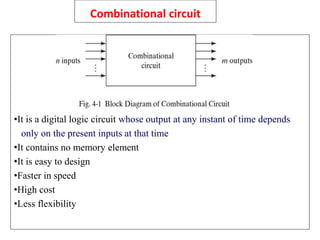
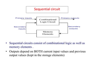
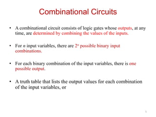
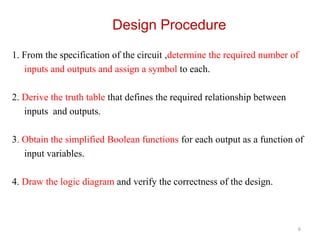
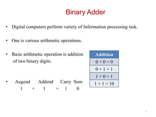
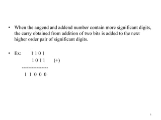
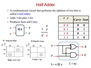
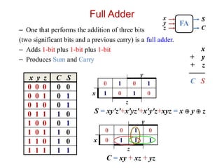
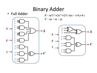
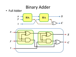
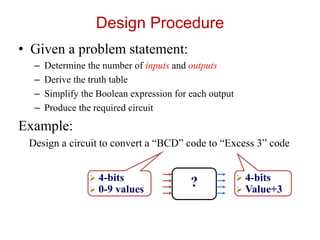
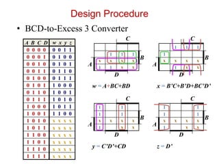
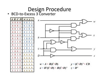
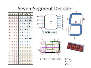
Combinational Circuits
D.Gopinath, AP/ECE
RIT, Rajapalayam
Academic Year 2020-21 ODD Semester
Combinational Circuits
• Design procedure
• Half adder & Full Adder
• Half subtractor & Full subtractor
• Parallel binary adder, parallel binary Subtractor
• Fast Adder - Carry Look Ahead adder
• Serial Adder/Subtractor
• BCD adder
• Binary Multiplier & Binary Divider
• Multiplexer/ Demultiplexer
• Decoder & encoder
• parity checker & parity generators
• code converters
• Magnitude Comparator.
Combinational circuit
•It is a digital logic circuit whose output at any instant of time depends
only on the present inputs at that time
•It contains no memory element
•It is easy to design
•Faster in speed
•High cost
•Less flexibility
• Sequential circuits consist of combinational logic as well as
memory elements .
• Outputs depend on BOTH current input values and previous
output values (kept in the storage elements)
Sequential circuit
Combinational Circuits
• A combinational circuit consists of logic gates whose outputs, at any
time, are determined by combining the values of the inputs.
• For n input variables, there are 2n possible binary input
combinations.
• For each binary combination of the input variables, there is one
possible output.
• A truth table that lists the output values for each combination
of the input variables, or
5
Design Procedure
1. From the specification of the circuit ,determine the required number of
inputs and outputs and assign a symbol to each.
2. Derive the truth table that defines the required relationship between
inputs and outputs.
3. Obtain the simplified Boolean functions for each output as a function of
input variables.
4. Draw the logic diagram and verify the correctness of the design.
6
Binary Adder
• Digital computers perform variety of Information processing task.
• One is various arithmetic operations.
• Basic arithmetic operation is addition
of two binary digits.
• Augend Addend Carry Sum
1 + 1 = 1 0
7
Addition
0 + 0 = 0
0 + 1 = 1
1 + 0 = 1
1 + 1 = 10
• When the augend and addend number contain more significant digits,
the carry obtained from addition of two bits is added to the next
higher order pair of significant digits.
• Ex: 1 1 0 1
1 0 1 1 (+)
----------------
1 1 0 0 0
8
Half Adder
– A combinational circuit that performs the addition of two bits is
called a half adder.
– Adds 1-bit plus 1-bit
– Produces Sum and Carry
x y
Carry Sum
0 0 0 0
0 1 0 1
1 0 0 1
1 1 1 0
x
+ y
───
C S
x
y
S
C
HA
x
y
S
C
S = x ⊕ y C = xy
Full Adder
– One that performs the addition of three bits
(two significant bits and a previous carry) is a full adder.
– Adds 1-bit plus 1-bit plus 1-bit
– Produces Sum and Carry
x y z C S
0 0 0 0 0
0 0 1 0 1
0 1 0 0 1
0 1 1 1 0
1 0 0 0 1
1 0 1 1 0
1 1 0 1 0
1 1 1 1 1
x
+ y
+ z
───
C S
FA
x
y
z
S
C
y
0 1 0 1
x 1 0 1 0
z
y
0 0 1 0
x 0 1 1 1
z
S = xy'z'+x'yz'+x'y'z+xyz = x  y  z
C = xy + xz + yz
Binary Adder
• Full Adder
x
y
z
S
C
x
y
x
z
y
z
x
y
z
x
y
z
x
y
z
x
y
z
x
y
z
x
y
z
x
y
x
z
y
z
S
C
S = xy'z'+x'yz'+x'y'z+xyz = x  y  z
C = xy + xz + yz
Binary Adder
• Full Adder
x
y
z
S
C
HA
x
y
z
HA S
C
Design Procedure
• Given a problem statement:
– Determine the number of inputs and outputs
– Derive the truth table
– Simplify the Boolean expression for each output
– Produce the required circuit
Example:
Design a circuit to convert a “BCD” code to “Excess 3” code
 4-bits
 0-9 values
 4-bits
 Value+3
?
Design Procedure
• BCD-to-Excess 3 Converter
A B C D w x y z
0 0 0 0 0 0 1 1
0 0 0 1 0 1 0 0
0 0 1 0 0 1 0 1
0 0 1 1 0 1 1 0
0 1 0 0 0 1 1 1
0 1 0 1 1 0 0 0
0 1 1 0 1 0 0 1
0 1 1 1 1 0 1 0
1 0 0 0 1 0 1 1
1 0 0 1 1 1 0 0
1 0 1 0 x x x x
1 0 1 1 x x x x
1 1 0 0 x x x x
1 1 0 1 x x x x
1 1 1 0 x x x x
1 1 1 1 x x x x
C
1 1 1
B
A
x x x x
1 1 x x
D
C
1 1 1
1
B
A
x x x x
1 x x
D
C
1 1
1 1
B
A
x x x x
1 x x
D
C
1 1
1 1
B
A
x x x x
1 x x
D
w = A+BC+BD x = B’C+B’D+BC’D’
y = C’D’+CD z = D’
Design Procedure
• BCD-to-Excess 3 Converter
A B C D w x y z
0 0 0 0 0 0 1 1
0 0 0 1 0 1 0 0
0 0 1 0 0 1 0 1
0 0 1 1 0 1 1 0
0 1 0 0 0 1 1 1
0 1 0 1 1 0 0 0
0 1 1 0 1 0 0 1
0 1 1 1 1 0 1 0
1 0 0 0 1 0 1 1
1 0 0 1 1 1 0 0
1 0 1 0 x x x x
1 0 1 1 x x x x
1 1 0 0 x x x x
1 1 0 1 x x x x
1 1 1 0 x x x x
1 1 1 1 x x x x
w
x
D
C
z
y
B
A
w = A + B(C+D)
x = B’(C+D) + B(C+D)’
y = (C+D)’ + CD
z = D’
Seven-Segment Decoder a
b
c
g
e
d
f
?
w
x
y
z
a
b
c
d
e
f
g
w x y z a b c d e f g
0 0 0 0 1 1 1 1 1 1 0
0 0 0 1 0 1 1 0 0 0 0
0 0 1 0 1 1 0 1 1 0 1
0 0 1 1 1 1 1 1 0 0 1
0 1 0 0 0 1 1 0 0 1 1
0 1 0 1 1 0 1 1 0 1 1
0 1 1 0 1 0 1 1 1 1 1
0 1 1 1 1 1 1 0 0 0 0
1 0 0 0 1 1 1 1 1 1 1
1 0 0 1 1 1 1 1 0 1 1
1 0 1 0 x x x x x x x
1 0 1 1 x x x x x x x
1 1 0 0 x x x x x x x
1 1 0 1 x x x x x x x
1 1 1 0 x x x x x x x
1 1 1 1 x x x x x x x
y
1 1 1
1 1 1
x
w
x x x x
1 1 x x
z
BCD code
a = w + y + xz + x’z’ b = . . .
c = . . .
d = . . .

COMBINATIONAL CIRCUITS

  • 1.
    Combinational Circuits D.Gopinath, AP/ECE RIT,Rajapalayam Academic Year 2020-21 ODD Semester
  • 2.
    Combinational Circuits • Designprocedure • Half adder & Full Adder • Half subtractor & Full subtractor • Parallel binary adder, parallel binary Subtractor • Fast Adder - Carry Look Ahead adder • Serial Adder/Subtractor • BCD adder • Binary Multiplier & Binary Divider • Multiplexer/ Demultiplexer • Decoder & encoder • parity checker & parity generators • code converters • Magnitude Comparator.
  • 3.
    Combinational circuit •It isa digital logic circuit whose output at any instant of time depends only on the present inputs at that time •It contains no memory element •It is easy to design •Faster in speed •High cost •Less flexibility
  • 4.
    • Sequential circuitsconsist of combinational logic as well as memory elements . • Outputs depend on BOTH current input values and previous output values (kept in the storage elements) Sequential circuit
  • 5.
    Combinational Circuits • Acombinational circuit consists of logic gates whose outputs, at any time, are determined by combining the values of the inputs. • For n input variables, there are 2n possible binary input combinations. • For each binary combination of the input variables, there is one possible output. • A truth table that lists the output values for each combination of the input variables, or 5
  • 6.
    Design Procedure 1. Fromthe specification of the circuit ,determine the required number of inputs and outputs and assign a symbol to each. 2. Derive the truth table that defines the required relationship between inputs and outputs. 3. Obtain the simplified Boolean functions for each output as a function of input variables. 4. Draw the logic diagram and verify the correctness of the design. 6
  • 7.
    Binary Adder • Digitalcomputers perform variety of Information processing task. • One is various arithmetic operations. • Basic arithmetic operation is addition of two binary digits. • Augend Addend Carry Sum 1 + 1 = 1 0 7 Addition 0 + 0 = 0 0 + 1 = 1 1 + 0 = 1 1 + 1 = 10
  • 8.
    • When theaugend and addend number contain more significant digits, the carry obtained from addition of two bits is added to the next higher order pair of significant digits. • Ex: 1 1 0 1 1 0 1 1 (+) ---------------- 1 1 0 0 0 8
  • 9.
    Half Adder – Acombinational circuit that performs the addition of two bits is called a half adder. – Adds 1-bit plus 1-bit – Produces Sum and Carry x y Carry Sum 0 0 0 0 0 1 0 1 1 0 0 1 1 1 1 0 x + y ─── C S x y S C HA x y S C S = x ⊕ y C = xy
  • 10.
    Full Adder – Onethat performs the addition of three bits (two significant bits and a previous carry) is a full adder. – Adds 1-bit plus 1-bit plus 1-bit – Produces Sum and Carry x y z C S 0 0 0 0 0 0 0 1 0 1 0 1 0 0 1 0 1 1 1 0 1 0 0 0 1 1 0 1 1 0 1 1 0 1 0 1 1 1 1 1 x + y + z ─── C S FA x y z S C y 0 1 0 1 x 1 0 1 0 z y 0 0 1 0 x 0 1 1 1 z S = xy'z'+x'yz'+x'y'z+xyz = x  y  z C = xy + xz + yz
  • 11.
    Binary Adder • FullAdder x y z S C x y x z y z x y z x y z x y z x y z x y z x y z x y x z y z S C S = xy'z'+x'yz'+x'y'z+xyz = x  y  z C = xy + xz + yz
  • 12.
    Binary Adder • FullAdder x y z S C HA x y z HA S C
  • 13.
    Design Procedure • Givena problem statement: – Determine the number of inputs and outputs – Derive the truth table – Simplify the Boolean expression for each output – Produce the required circuit Example: Design a circuit to convert a “BCD” code to “Excess 3” code  4-bits  0-9 values  4-bits  Value+3 ?
  • 14.
    Design Procedure • BCD-to-Excess3 Converter A B C D w x y z 0 0 0 0 0 0 1 1 0 0 0 1 0 1 0 0 0 0 1 0 0 1 0 1 0 0 1 1 0 1 1 0 0 1 0 0 0 1 1 1 0 1 0 1 1 0 0 0 0 1 1 0 1 0 0 1 0 1 1 1 1 0 1 0 1 0 0 0 1 0 1 1 1 0 0 1 1 1 0 0 1 0 1 0 x x x x 1 0 1 1 x x x x 1 1 0 0 x x x x 1 1 0 1 x x x x 1 1 1 0 x x x x 1 1 1 1 x x x x C 1 1 1 B A x x x x 1 1 x x D C 1 1 1 1 B A x x x x 1 x x D C 1 1 1 1 B A x x x x 1 x x D C 1 1 1 1 B A x x x x 1 x x D w = A+BC+BD x = B’C+B’D+BC’D’ y = C’D’+CD z = D’
  • 15.
    Design Procedure • BCD-to-Excess3 Converter A B C D w x y z 0 0 0 0 0 0 1 1 0 0 0 1 0 1 0 0 0 0 1 0 0 1 0 1 0 0 1 1 0 1 1 0 0 1 0 0 0 1 1 1 0 1 0 1 1 0 0 0 0 1 1 0 1 0 0 1 0 1 1 1 1 0 1 0 1 0 0 0 1 0 1 1 1 0 0 1 1 1 0 0 1 0 1 0 x x x x 1 0 1 1 x x x x 1 1 0 0 x x x x 1 1 0 1 x x x x 1 1 1 0 x x x x 1 1 1 1 x x x x w x D C z y B A w = A + B(C+D) x = B’(C+D) + B(C+D)’ y = (C+D)’ + CD z = D’
  • 16.
    Seven-Segment Decoder a b c g e d f ? w x y z a b c d e f g wx y z a b c d e f g 0 0 0 0 1 1 1 1 1 1 0 0 0 0 1 0 1 1 0 0 0 0 0 0 1 0 1 1 0 1 1 0 1 0 0 1 1 1 1 1 1 0 0 1 0 1 0 0 0 1 1 0 0 1 1 0 1 0 1 1 0 1 1 0 1 1 0 1 1 0 1 0 1 1 1 1 1 0 1 1 1 1 1 1 0 0 0 0 1 0 0 0 1 1 1 1 1 1 1 1 0 0 1 1 1 1 1 0 1 1 1 0 1 0 x x x x x x x 1 0 1 1 x x x x x x x 1 1 0 0 x x x x x x x 1 1 0 1 x x x x x x x 1 1 1 0 x x x x x x x 1 1 1 1 x x x x x x x y 1 1 1 1 1 1 x w x x x x 1 1 x x z BCD code a = w + y + xz + x’z’ b = . . . c = . . . d = . . .

Editor's Notes

  • #6 5
  • #10 4241 - Digital Logic Design
  • #11 4241 - Digital Logic Design
  • #12 4241 - Digital Logic Design
  • #13 4241 - Digital Logic Design
  • #14 4241 - Digital Logic Design
  • #15 4241 - Digital Logic Design
  • #16 4241 - Digital Logic Design
  • #17 4241 - Digital Logic Design