This document discusses various combinational and sequential logic blocks used in digital circuit design. It covers topics like adders, subtractors, multipliers, multiplexers, demultiplexers, decoders, encoders, flip-flops, registers, counters and finite state machines. It provides details on the design and working of different logic blocks like half adder, full adder, binary adder, magnitude comparator, encoder, decoder etc. with truth tables and logic diagrams. Examples are given to illustrate the implementation of logic functions using decoders and multiplexers.
Combination of circuit full ppt explainationhdhdjdkdjjdjdidididiisisiskkssjisshsuusushjwiwuueueuududhdndnd djdjdjje eurhebbe rudjenr r r earned d reuudbe d re eendbeuee ruebrbe r dudijsjsbd druirrndjidd didoosowkws eosooedknd eeiidkdididiidndndjd
Idjdjjdjjf fduudjdhdjjsb suejejen duejjebebb eiireiej nenndskaoaosowghdhdh
Jdjjddddddudjdjjsjaks shuddh djd d dudisiss sjaja dijdjdbddus
Read| The latest issue of The Challenger is here! We are thrilled to announce that our school paper has qualified for the NATIONAL SCHOOLS PRESS CONFERENCE (NSPC) 2024. Thank you for your unwavering support and trust. Dive into the stories that made us stand out!
Welcome to TechSoup New Member Orientation and Q&A (May 2024).pdfTechSoup
In this webinar you will learn how your organization can access TechSoup's wide variety of product discount and donation programs. From hardware to software, we'll give you a tour of the tools available to help your nonprofit with productivity, collaboration, financial management, donor tracking, security, and more.
Introduction to AI for Nonprofits with Tapp NetworkTechSoup
Dive into the world of AI! Experts Jon Hill and Tareq Monaur will guide you through AI's role in enhancing nonprofit websites and basic marketing strategies, making it easy to understand and apply.
The Roman Empire A Historical Colossus.pdfkaushalkr1407
The Roman Empire, a vast and enduring power, stands as one of history's most remarkable civilizations, leaving an indelible imprint on the world. It emerged from the Roman Republic, transitioning into an imperial powerhouse under the leadership of Augustus Caesar in 27 BCE. This transformation marked the beginning of an era defined by unprecedented territorial expansion, architectural marvels, and profound cultural influence.
The empire's roots lie in the city of Rome, founded, according to legend, by Romulus in 753 BCE. Over centuries, Rome evolved from a small settlement to a formidable republic, characterized by a complex political system with elected officials and checks on power. However, internal strife, class conflicts, and military ambitions paved the way for the end of the Republic. Julius Caesar’s dictatorship and subsequent assassination in 44 BCE created a power vacuum, leading to a civil war. Octavian, later Augustus, emerged victorious, heralding the Roman Empire’s birth.
Under Augustus, the empire experienced the Pax Romana, a 200-year period of relative peace and stability. Augustus reformed the military, established efficient administrative systems, and initiated grand construction projects. The empire's borders expanded, encompassing territories from Britain to Egypt and from Spain to the Euphrates. Roman legions, renowned for their discipline and engineering prowess, secured and maintained these vast territories, building roads, fortifications, and cities that facilitated control and integration.
The Roman Empire’s society was hierarchical, with a rigid class system. At the top were the patricians, wealthy elites who held significant political power. Below them were the plebeians, free citizens with limited political influence, and the vast numbers of slaves who formed the backbone of the economy. The family unit was central, governed by the paterfamilias, the male head who held absolute authority.
Culturally, the Romans were eclectic, absorbing and adapting elements from the civilizations they encountered, particularly the Greeks. Roman art, literature, and philosophy reflected this synthesis, creating a rich cultural tapestry. Latin, the Roman language, became the lingua franca of the Western world, influencing numerous modern languages.
Roman architecture and engineering achievements were monumental. They perfected the arch, vault, and dome, constructing enduring structures like the Colosseum, Pantheon, and aqueducts. These engineering marvels not only showcased Roman ingenuity but also served practical purposes, from public entertainment to water supply.
Unit 8 - Information and Communication Technology (Paper I).pdfThiyagu K
This slides describes the basic concepts of ICT, basics of Email, Emerging Technology and Digital Initiatives in Education. This presentations aligns with the UGC Paper I syllabus.
Model Attribute Check Company Auto PropertyCeline George
In Odoo, the multi-company feature allows you to manage multiple companies within a single Odoo database instance. Each company can have its own configurations while still sharing common resources such as products, customers, and suppliers.
Acetabularia Information For Class 9 .docxvaibhavrinwa19
Acetabularia acetabulum is a single-celled green alga that in its vegetative state is morphologically differentiated into a basal rhizoid and an axially elongated stalk, which bears whorls of branching hairs. The single diploid nucleus resides in the rhizoid.
The French Revolution, which began in 1789, was a period of radical social and political upheaval in France. It marked the decline of absolute monarchies, the rise of secular and democratic republics, and the eventual rise of Napoleon Bonaparte. This revolutionary period is crucial in understanding the transition from feudalism to modernity in Europe.
For more information, visit-www.vavaclasses.com
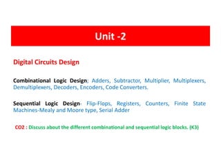
1. Unit -2
Digital Circuits Design
Combinational Logic Design; Adders, Subtractor, Multiplier, Multiplexers,
Demultiplexers, Decoders, Encoders, Code Converters.
Sequential Logic Design- Flip-Flops, Registers, Counters, Finite State
Machines-Mealy and Moore type, Serial Adder
CO2 : Discuss about the different combinational and sequential logic blocks. (K3)
15. Carry-Look Ahead Adder
Gi = AiBi
Pi = Ai ⊕Bi
Gi is known as the carry Generate signal
Pi is known as the carry propagate signal
Si = Pi ⊕ Ci
Ci+1 = Gi + PiCi
34. Multiplexer
• A MUX is a digital switch that has
multiple inputs (sources) and a single
output (destination).
• The select lines determine which input
is connected to the output.
• MUX Types
2-to-1 (1 select line)
4-to-1 (2 select lines)
8-to-1 (3 select lines)
16-to-1 (4 select lines)
Select Lines
Inputs
(sources)
Output
(destination)
1
2N
N
MUX
47. Encoder
An encoder is a circuit that accepts many inputs and generates the output
in a coded form. Encoder is a device which has 2n' inputs and 'n' numberof
output
48. • Adecoder is a combinational circuit.
• A decoder accepts a set of inputs that represents a binary number and
activates only that output corresponding to the input number.All other
outputs remain inactive.
• There are 2N possible input combinations, for each of these input
combination only one output will be HIGH (active) all other outputs are
LOW
• Some decoder have one or more ENABLE (E) inputs that are used to control
the operation of decoder.
Decoder
49. BLOCK DIAGRAM OF DECODER
DECODER
A0
A1
A2
AN-1
.
.
.
.
N- Inputs M- Outputs
Only one output is High for
each input
.
.
.
.
B0
B1
B2
BM-1
50. 2 to 4 Line Decoder:
Block diagram of 2 to 4 decoder is shown in fig.
Aand B are the inputs. ( No. of inputs =2)
No. of possible input combinations: 22=4
No. of Outputs : 22=4, they are indicated by D0, D1, D2 and D3
From the Truth Table it is clear that each output is “1” for only specific
combination of inputs.
A
B
0
D
D1
D2
3
2 X 4
Decoder
INPUTS OUTPUTS
A B D0 D1 D2 D3
0 0 1 0 0 0
0 1 0 1 0 0
1 0 0 0 1 0
1 1 0 0 0 1
TRUTH TABLE
Inputs
D
Outputs
51. BOOLEAN EXPRESSION:
From Truth Table
D0 A B
D2 A B
LOGIC DIAGRAM:
D1 A B
D3 AB
A
A B
B
D0 AB
D1 A B
D2 A B
D3 A B
52. 3 to 8 Line Decoder:
Block diagram of 3 to 8 decoder is shown in fig
A, B and C are the inputs. ( No. of inputs =3)
No. of possible input combinations: 23=8
No. of Outputs : 23=8, they are indicated by D0 to D7
From the Truth Table it is clear that each output is “1” for only specific
combination of inputs.
3 X 8
Decoder
A
B
C
. D0
.
.
.
D7
Outputs
Inputs
54. LOGIC DIAGRAM OF 3 X 8 DECODER:
D0 A B C
D1 A B C
D2 A B C
D3 A B C
D4 A B C
D5 A B C
D6 A B C
D7 A B C
A B C
OUTPUTS
INPUTS
A B C
55. 3 x 8 Decoder From 2 x 4 Decoder:
2 x 4 Decoder
2 x 4 Decoder
X
Y
E'
D0
D1
D2
D3
D4
D5
D6
D7
OUTPUT
INPUT
56. 2
3
4
5
6
7
Example: Implement the following multiple output function using a suitable
Decoder.
f1(A, B, C) = ∑m(0,4,7)+ d(2,3)
f2 (A, B, C) =∑m (1,5,6)
f3 (A, B, C) =∑m (0,2,4,6)
Solution: f1 consists of don’t care conditions. So we consider them to be logic 1.
0
1
f1(A, B, C)
f2 (A, B, C)
f3 (A, B, C)
3
x
8
Decoder
A
B
C
INPUTS
57. EXAMPLE: Implement the following Boolean function using suitable Decoder.
f1 (x,y,z)=∑m(1,5,7)
f2 (x,y,z)=∑m(0,3)
f3 (x,y,z)=∑m(2,4,5)
Solution:
X
Y
Z
E
3
X
8
Decoder
0
1
2
3
4
5
6
7
INPUTS
f1 (x,y,z)
f2 (x,y,z)
f3 (x,y,z)
58. F1 (x, y ,z ) x y z x z
F2 (x, y,z) x y z x z
SOLUTION: STEP 1: Write the given function F1 in SOP form
F1(x, y,z) x y z (y y ) x z
F1(x, y,z) x y z x y z x y z
F1(x, y,z) m (0,5,7)
F2 (x, y,z) x y z x z
F2 (x, y,z) x y z (y y ) x z
F2 (x, y,z) x y z x y z x y z
F2 (x, y,z) m (1,3,6)
Implementation using Decoder
60. ENCODER
• An Encoder is a combinational logic circuit.
• It performs the inverse operation of Decoder.
• The opposite process of decoding is known as Encoding.
• An Encoder converts an active input signal into a coded output signal.
• Block diagram of Encoder is shown in Fig.10. It has ‘M’ inputs and ‘N’
outputs.
• An Encoder has ‘M’ input lines, only one of which is activated at a given
time, and produces an N-bit output code, depending on which input is
activated.
-
-
-
-
-
-
-
-
-
-
-
-
-
-
‘M’
Inputs
‘N’
Outputs
Encoder
A0
A1
A2
AM-1
B0
B1
B2
BN-1
61. • Encoders are used to translate the rotary or linear motion into a digital
signal.
• The difference between Decoder and Encoder is that Decoder has Binary
Code as an input while Encoder has Binary Code as an output.
• Encoder is an Electronics device that converts the analog signal to digital
signal such as BCD Code.
• Types of Encoders
i. Priority Encoder
ii. Decimal to BCD Encoder
iii. Octal to Binary Encoder
iv. Hexadecimal to Binary Encoder
62. Encoder
4 x 2
Decoder
2 x 4
A0
A1
A2
A3
M=4
M=22
M=2N
‘M’is the input and
‘N’is the output
B0
B1
B2
B3
66. PRIORITY ENCODER:
• As the name indicates, the priority is given to inputs line.
• If two or more input lines are high at the same time i.e 1 at the same time, then
the input line with high priority shall be considered.
D3
D2
D1
D0
Y1
Y0
Highest Priority
Input
Priority
Encoder
Lowest Priority Output
Input
Block Diagram of Priority
Encoder
INPUTS OUTPUTS V
D3 D2 D1 D0 Y1 Y0
0 0 0 0 x x 0
0 0 0 1 0 0 1
0 0 1 x 0 1 1
0 1 x x 1 0 1
1 x x x 1 1 1
TRUTH TABLE:
67. X 0 0 0
1 1 1 1
1 1 1 1
1 1 1 1
00
01
11
10 10
11
01
00 X 0 1 1
0 0 0 0
1 1 1 1
1 1 1 1
D3D2
D3D2
D1D0
D1D0
00 01 11 10 00 01 11 10
2 1
3
0
Y D D D
• There are four inputs D0, D1,D2, D3 and two outputsY1 and Y2.
• D3 has highest priority and D0 is at lowest priority.
• If D3=1 irrespective of other inputs then outputY1Y0=11.
• D3 is at highest priority so other inputs are considered as don’t care.
Y1 D2 D3
69. DECIMAL TO BCD ENCODER:
• It has ten inputs corresponding to ten decimal digits (from 0 to 9) and four
outputs (A,B,C,D) representing the BCD.
-
-
-
-
-
-
-
-
-
ENCODER
C
0
1
2
9
INPUTS
A
B
D
OUTPUTS
89. Memory Elements
• The desired operation is that the alarm turns on when the sensor generates a
positive voltage signal, Set, in response to some event.
• Once the alarm is triggered, it must remain active even if the sensor output
goes back to zero.
• The alarm is turned off manually by means of a Reset input.
• The circuit requires a memory element to remember that the alarm has to be
active until the Reset signal arrives
90. Latch
A Latch is a special type of logical circuit. The latches have low and high two
stable states. Due to these states, latches also refer to as bistable-
multivibrators. A latch is a storage device that holds the data using the
feedback lane
93. Gated SR Latch
To ensure a meaningful operation of the gated SR latch, it is essential to avoid
the possibility of having both the S and R inputs equal to 1 when Clk changes
from 1 to 0.
95. Classification
• SR Latch
• Gated S-R Latch
• D latch
• Gated D Latch
• JK Latch
• T Latch.
Latch Flip Flop
• SR Flip-Flop
• D Flip-Flop
• JK Flip-Flop
• T Flip-Flop
106. Flip Flops Conversion
In the previous Class, we discussed the four flip-flops, namely SR flip-
flop, D flip-flop, JK flip-flop & T flip-flop.
We can convert one flip-flop into the remaining three flip-flops by
including some additional logic. So, there will be total of twelve flip-flop
conversions.
• JK flip-flop to T flip-flop
• JK flip-flop to D flip-flop
• JK flip-flop to SR flip-flop
• T flip-flop to D flip-flop
• T flip-flop to SR flip-flop
• T flip-flop to JK flip-flop
• D flip-flop to T flip-flop
• D flip-flop to SR flip-flop
• D flip-flop to JK flip-flop
• SR flip-flop to D flip-flop
• SR flip-flop to JK flip-flop
• SR flip-flop to T flip-flop