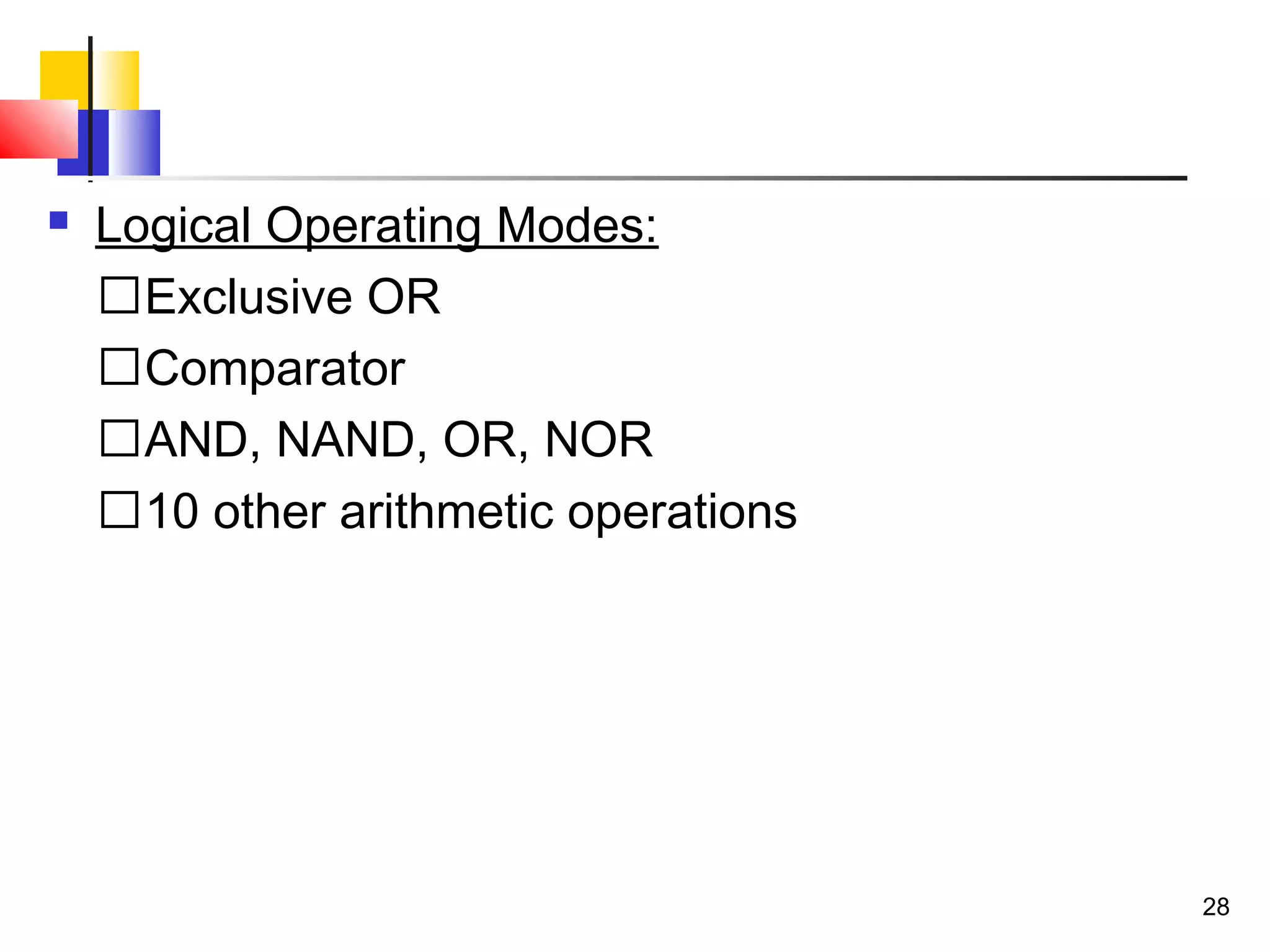
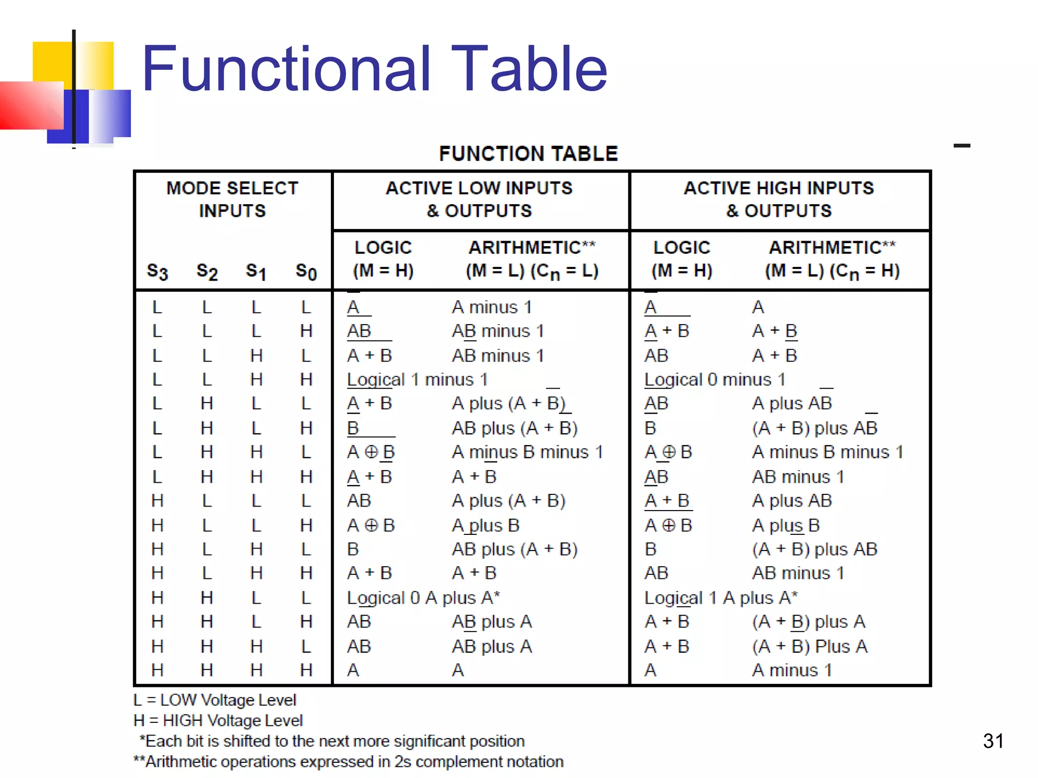
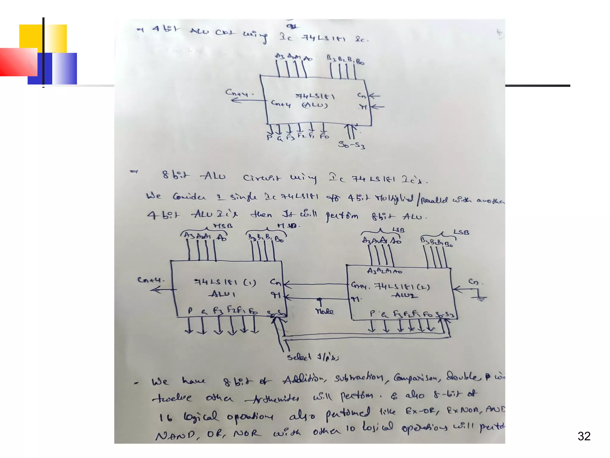
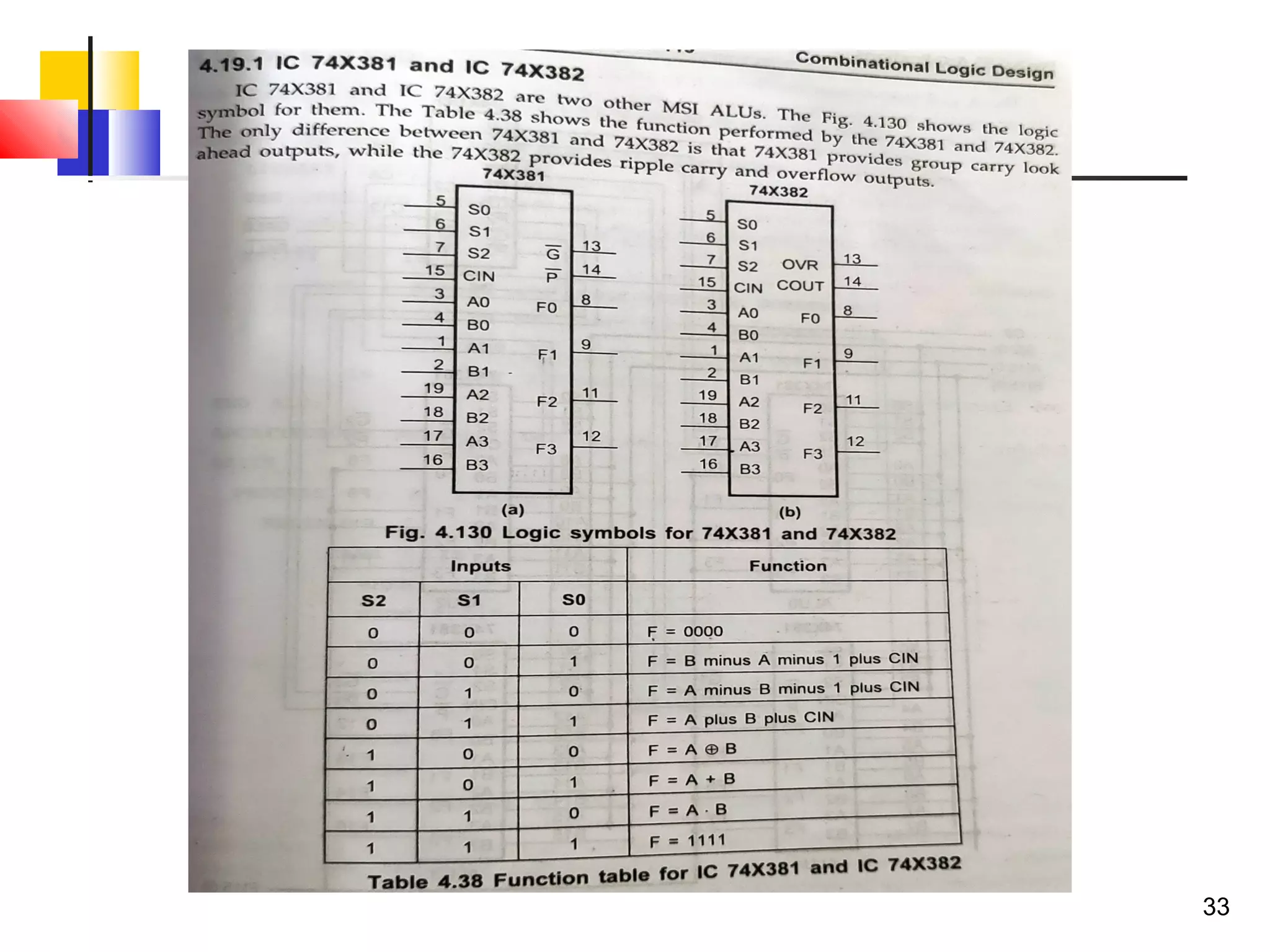
Downloaded 88 times


![1/8/2012 - L3 Data
Path Design
Copyright 2006 - Joanne
DeGroat, ECE, OSU 29
ALU Operations (integer
ALU)
Add (A+B)
Add with Carry (A+B+Cin)
Subtract (A-B)
Subtract with Borrow (A-B-Cin)
[Subract reverse (B-A)]
[Subract reverse with Borrow (B-A-
Cin)]
Negative A (-A)
Negative B (-B)
Increment A (A+1)
Increment B (B+1)
Decrement A (A-1)
Decrement B (B-1)
Logical AND
Logical OR
Logical XOR
Not A
Not B
A
B
Multiply Step or Multiply
Divide Step or Divide
Mask
Conditional AND/OR (uses
Mask)
Shift
Zero](https://image.slidesharecdn.com/unit4dica-180906162330/75/Unit-4-dica-29-2048.jpg)


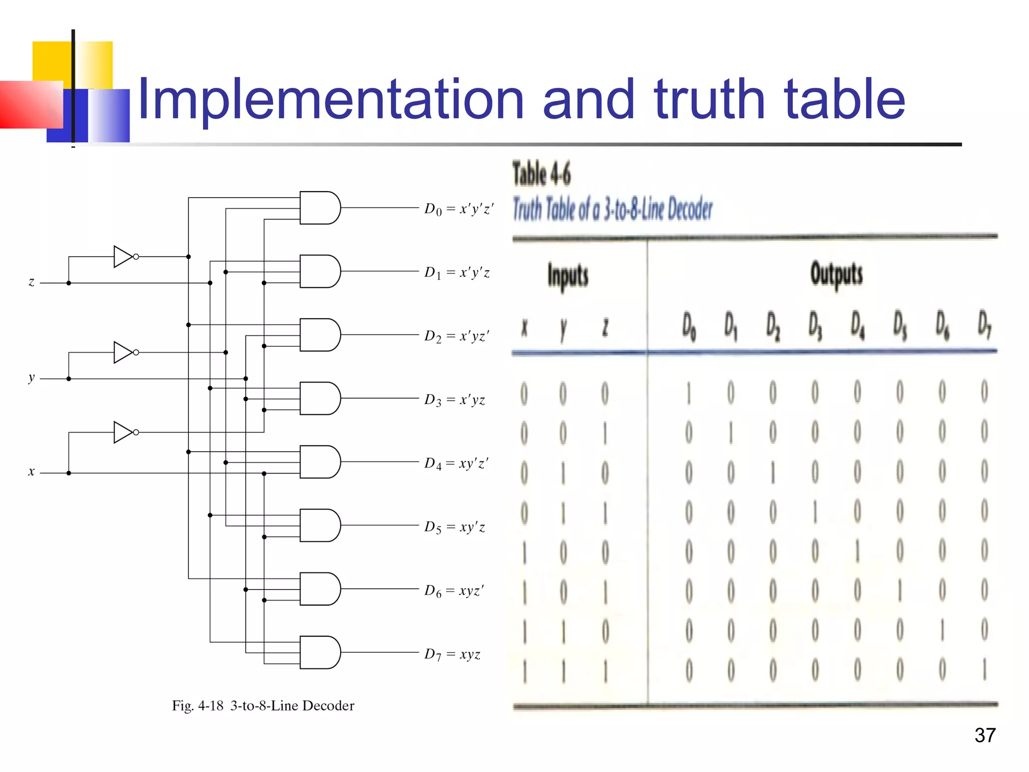
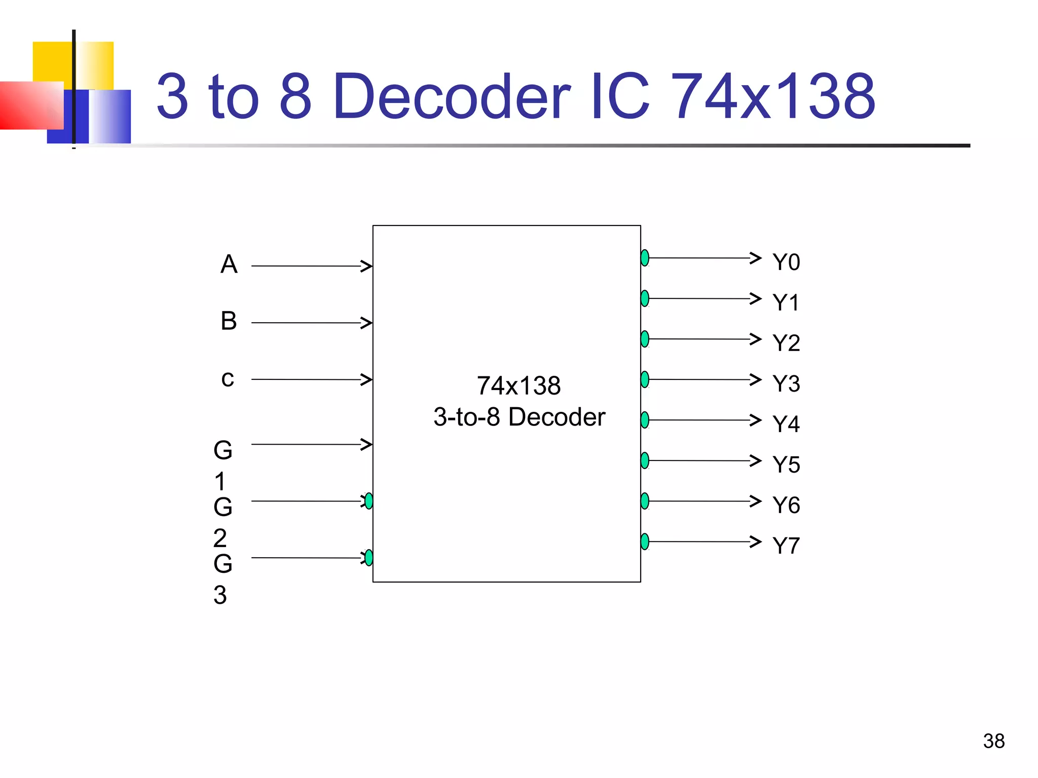


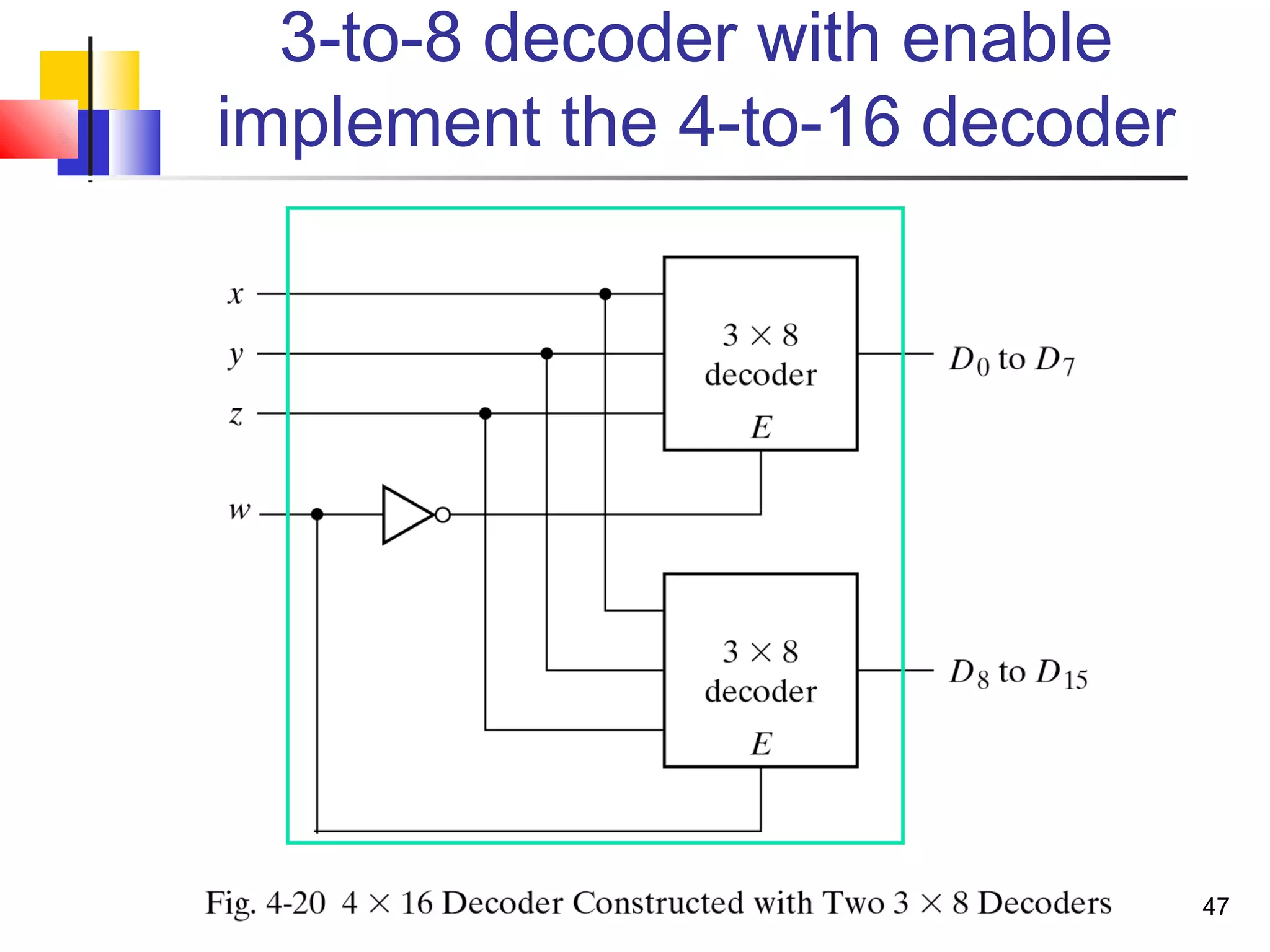


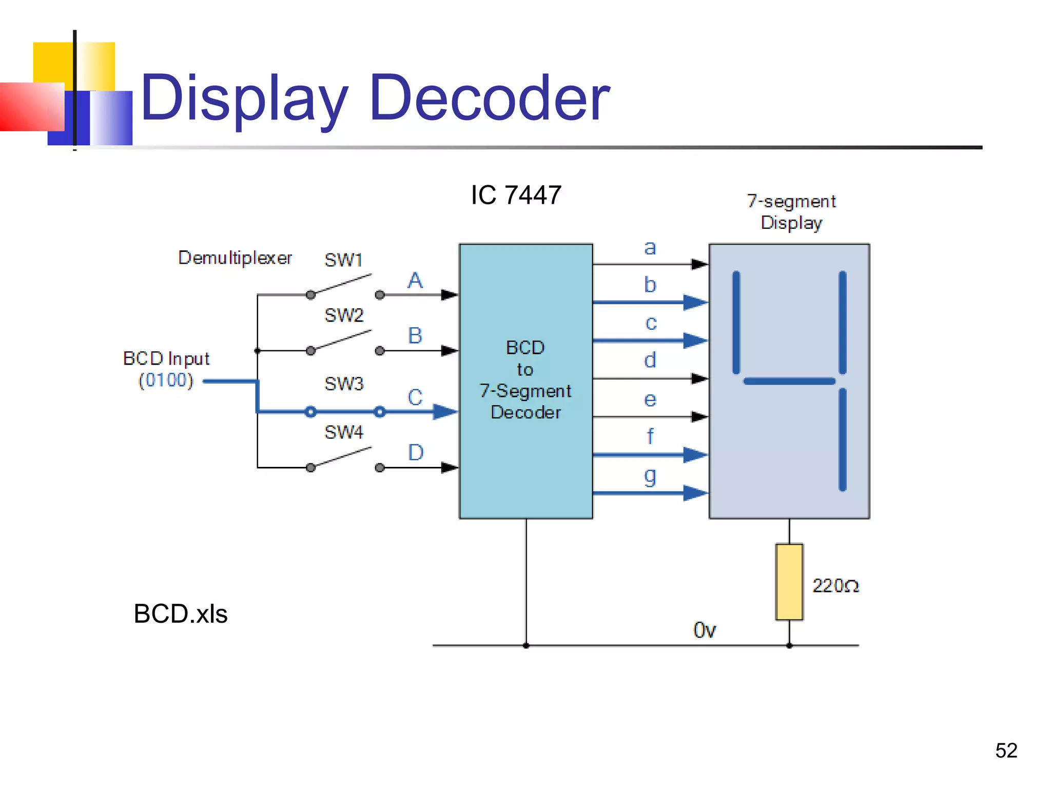
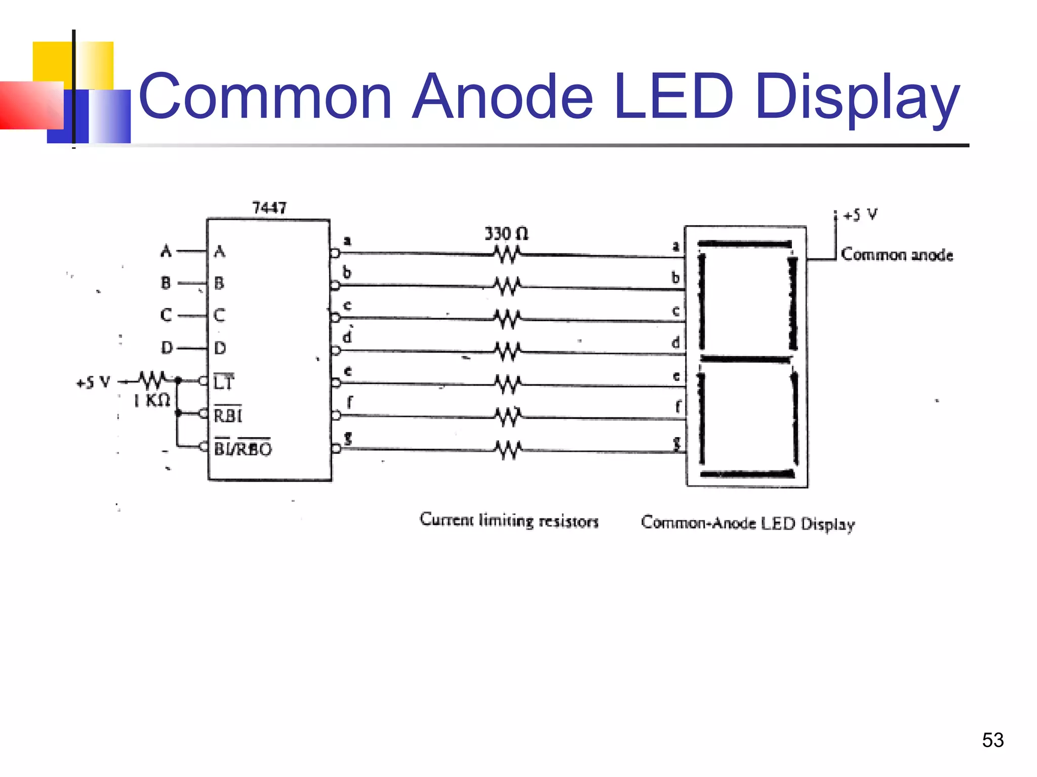

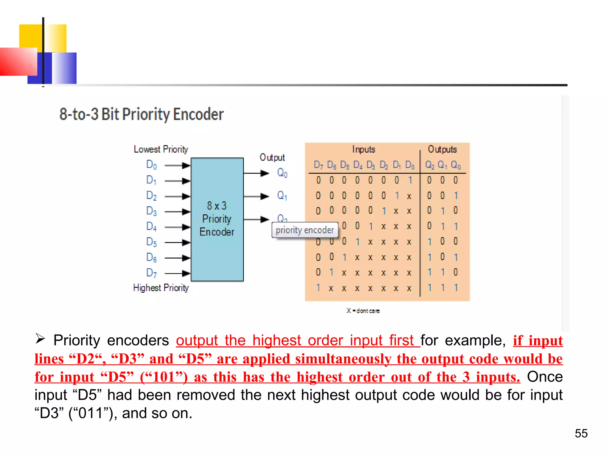

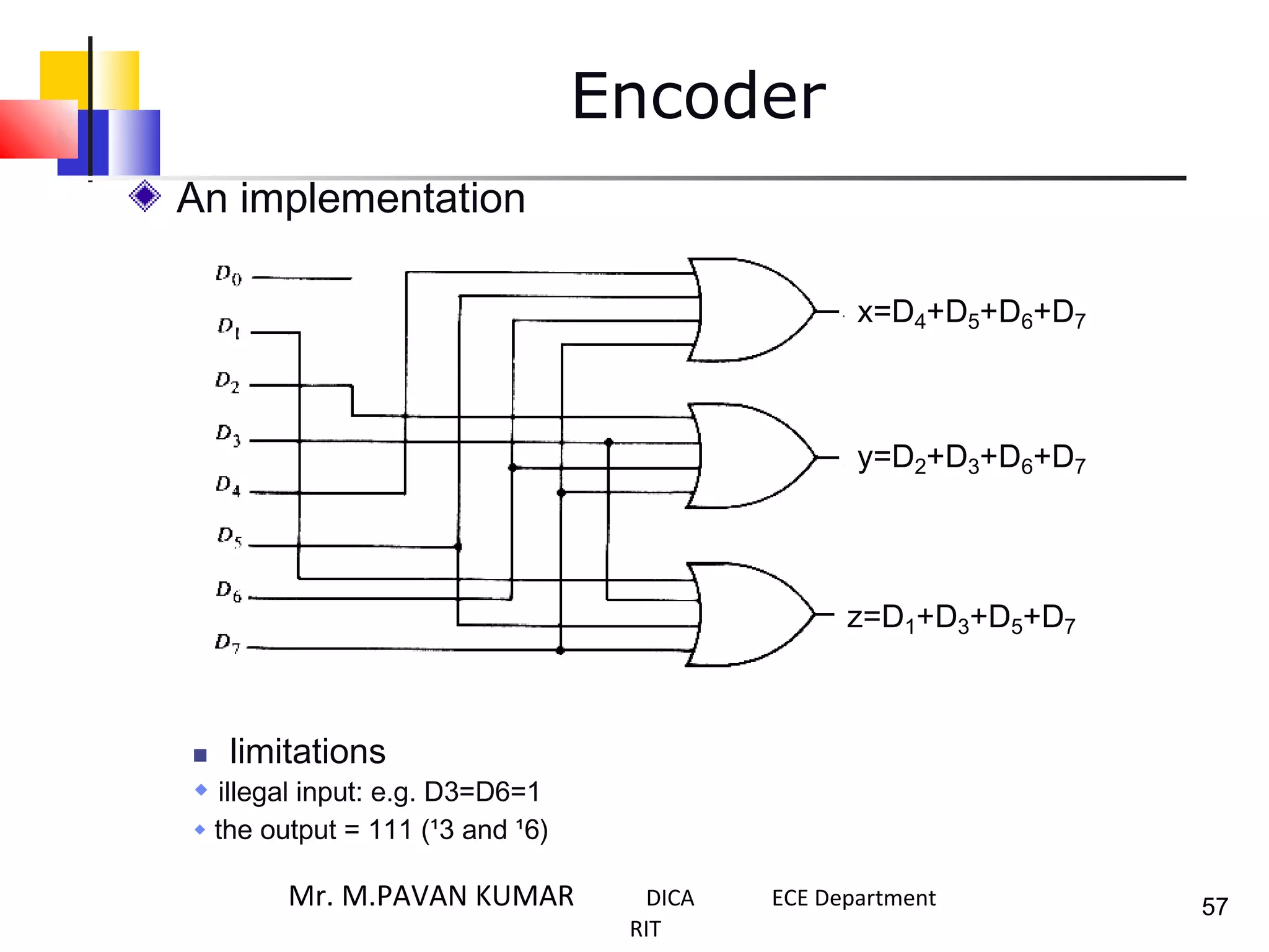


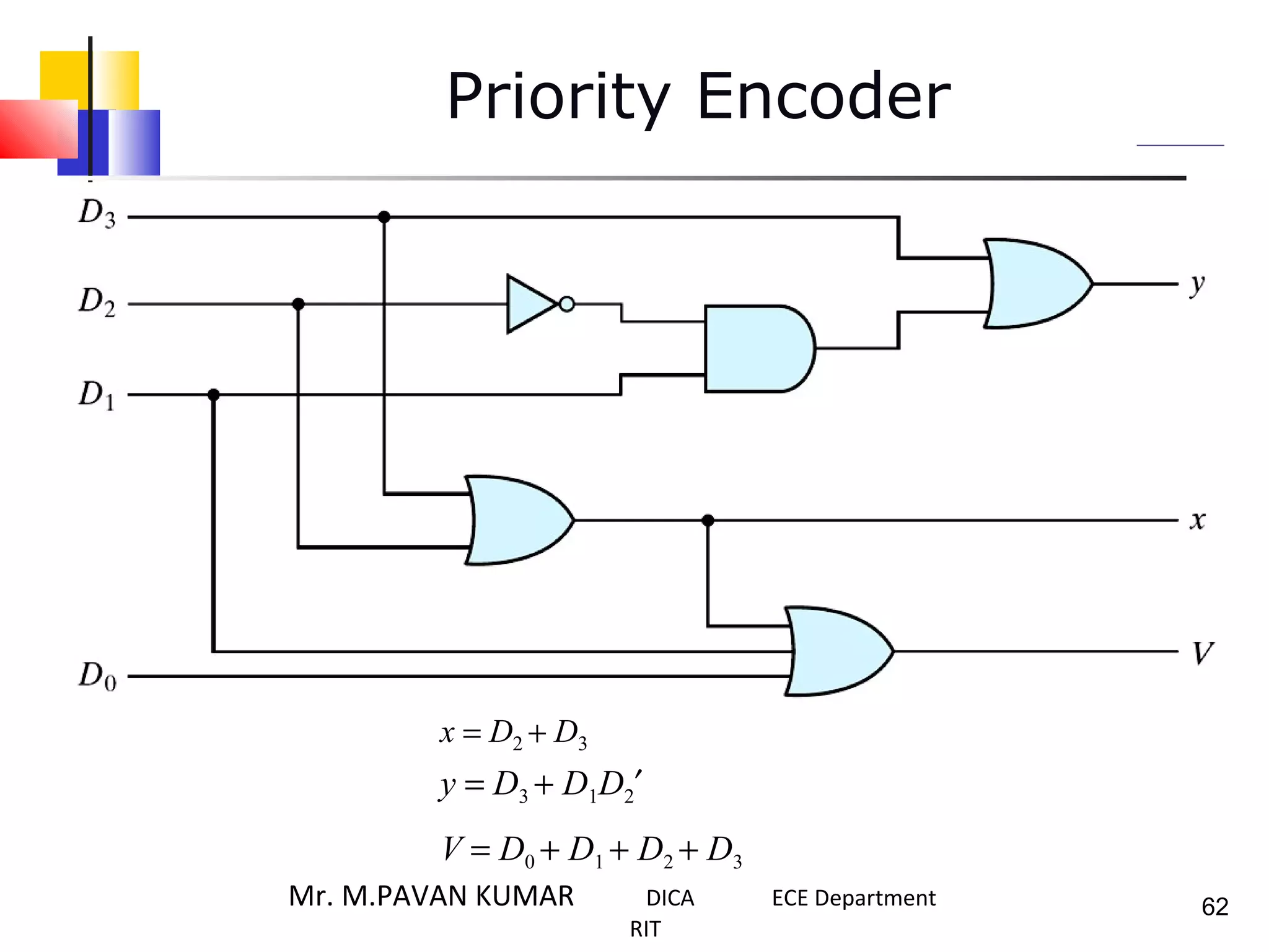

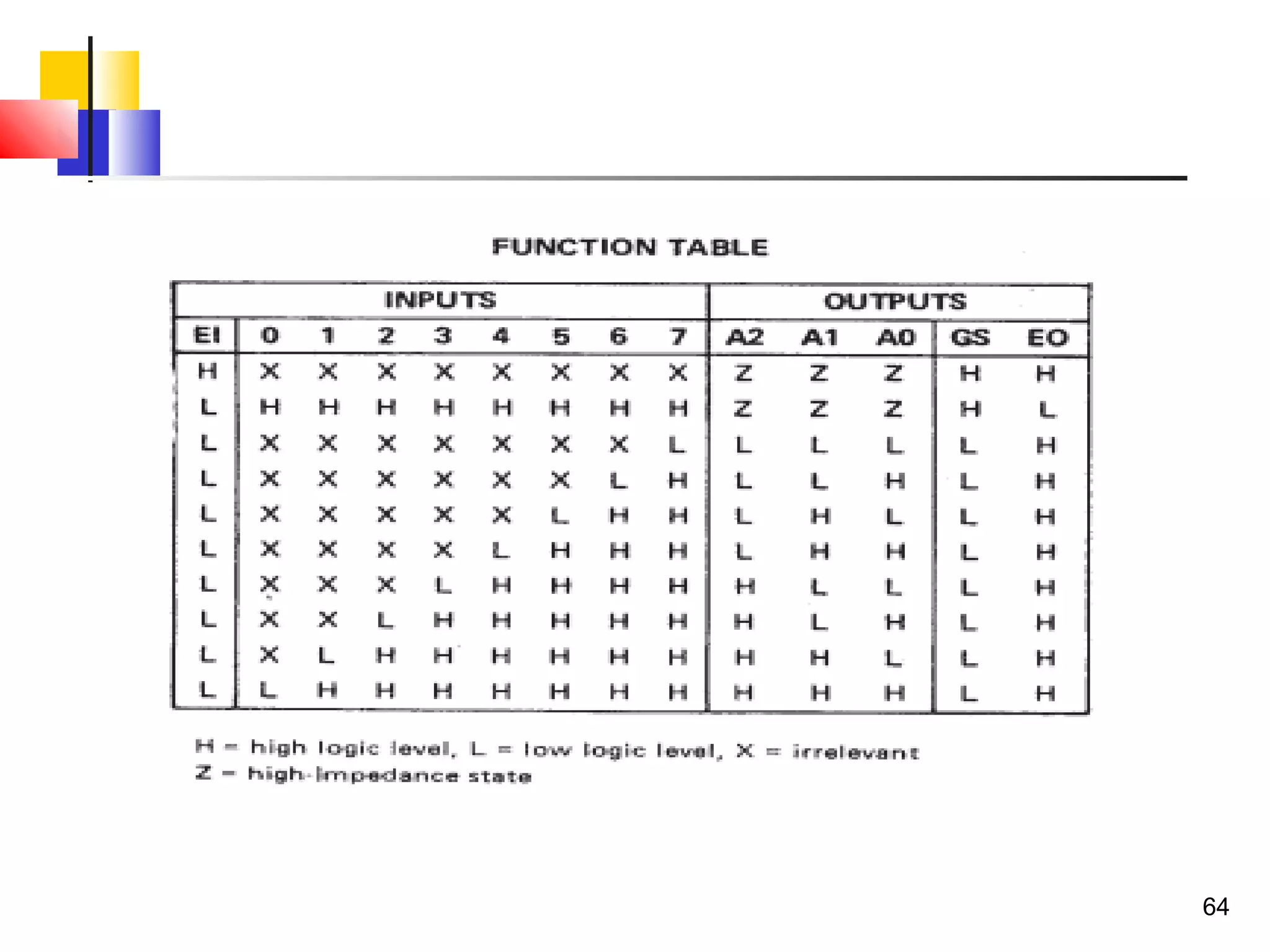


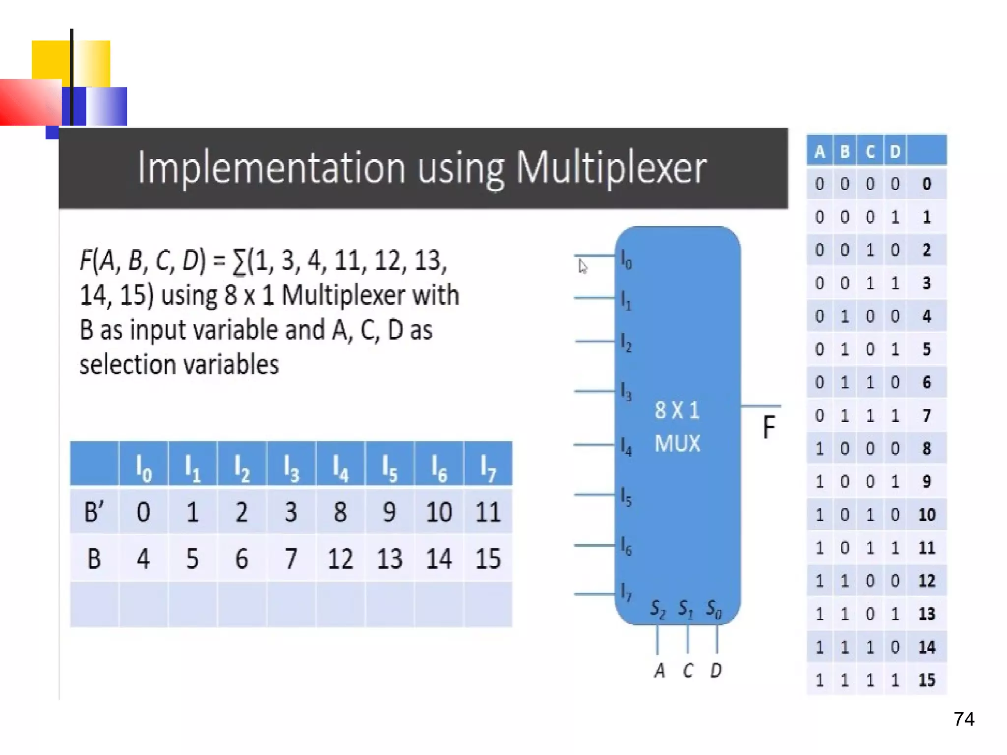


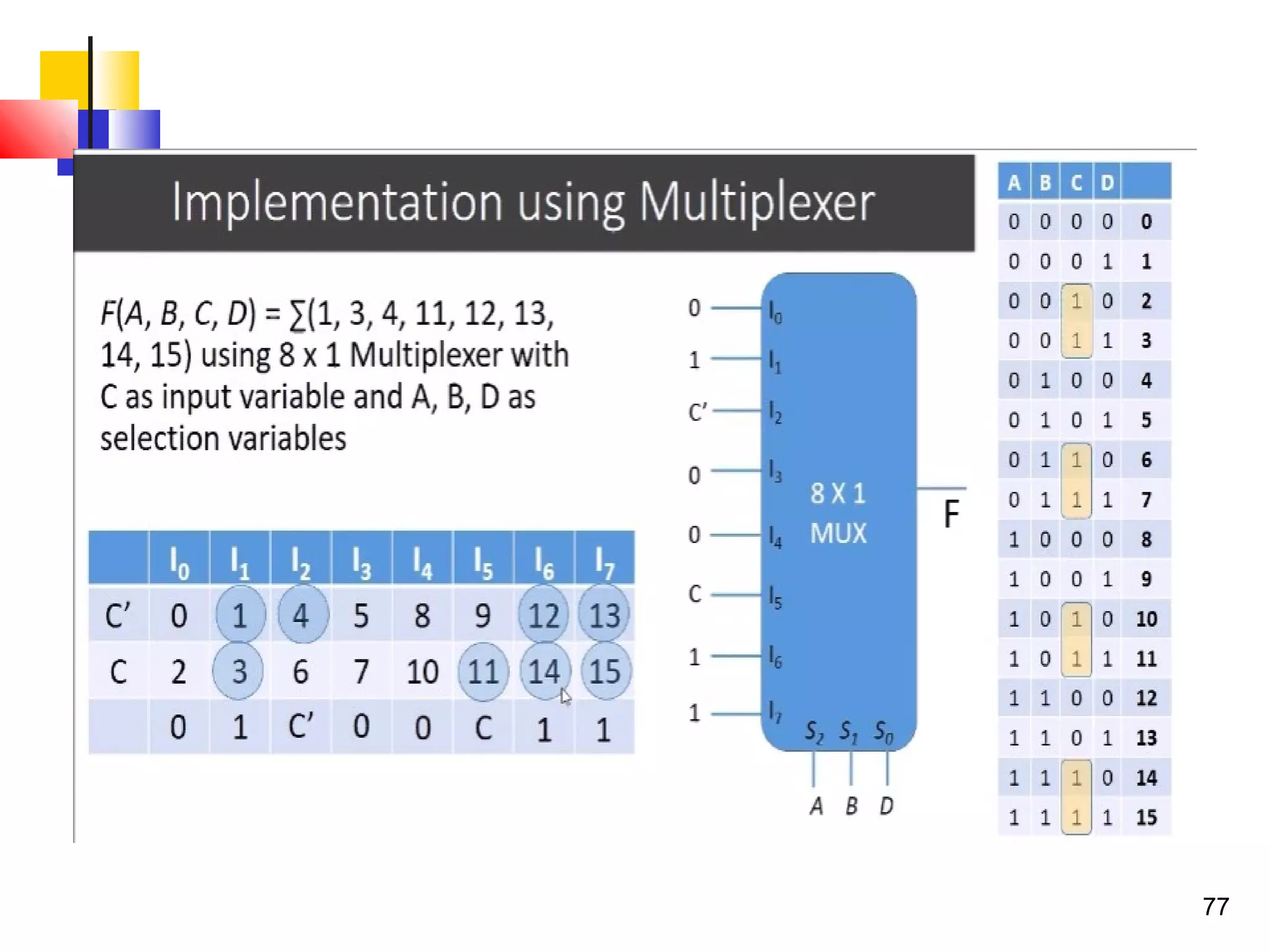

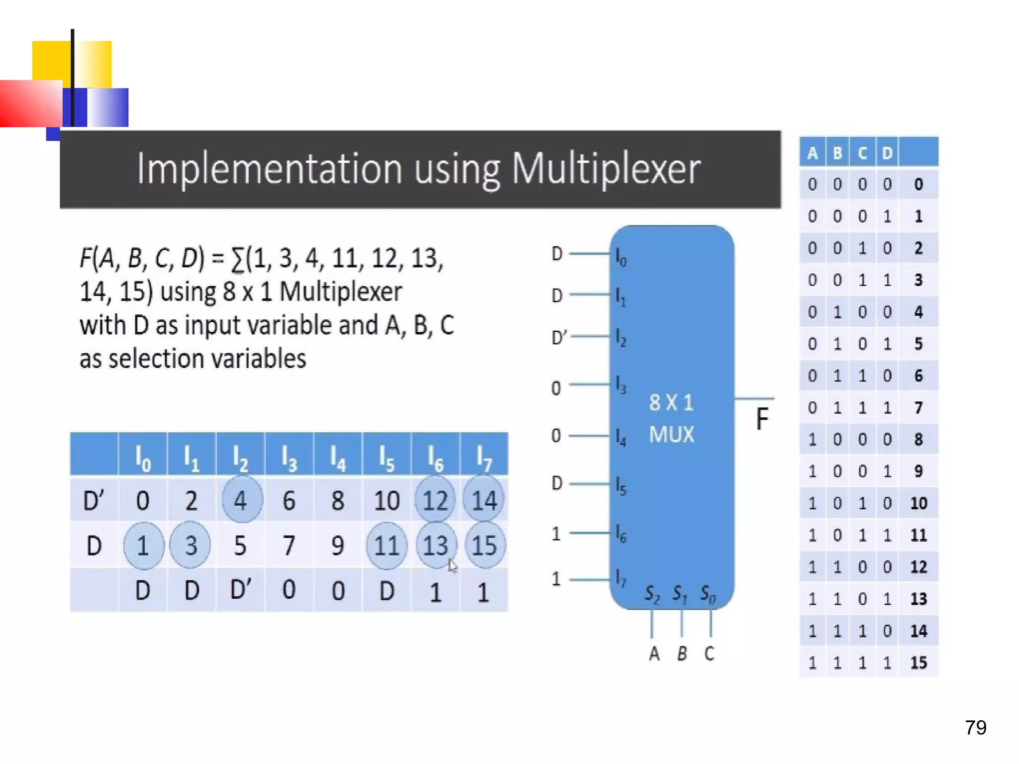

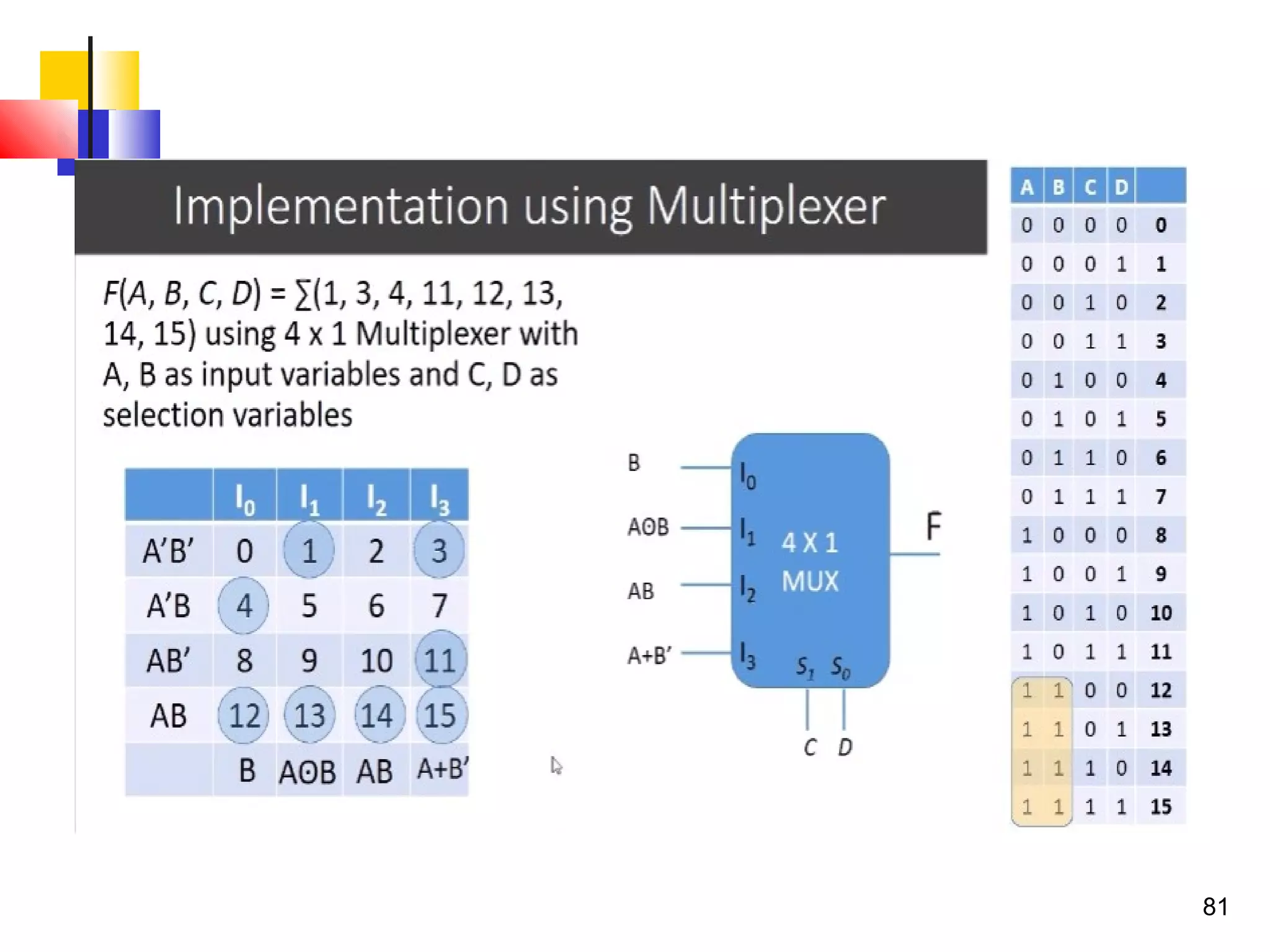

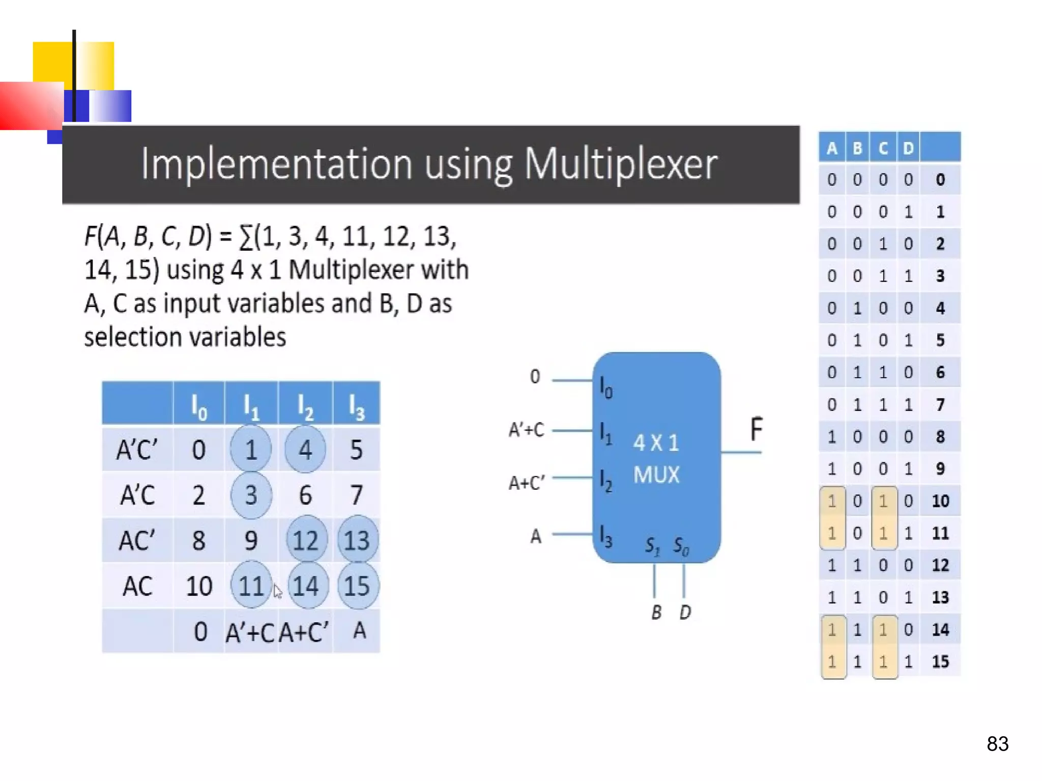
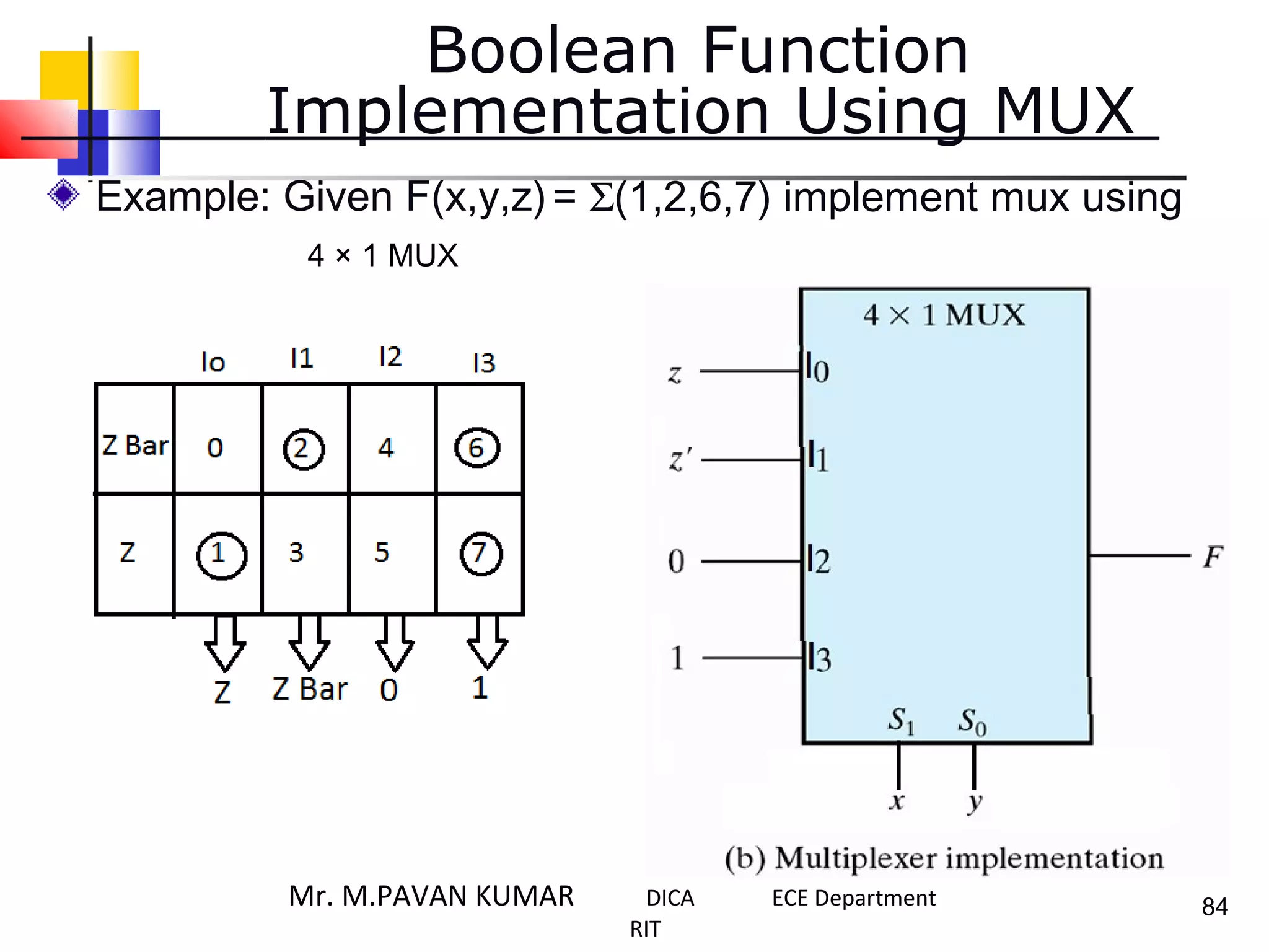

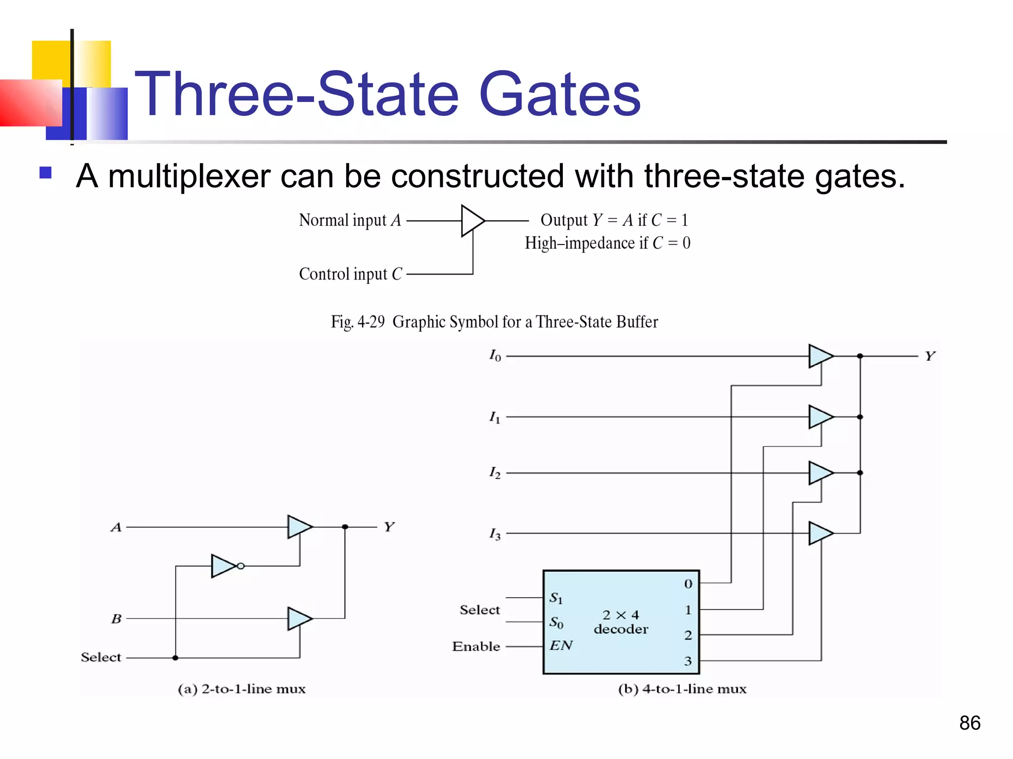
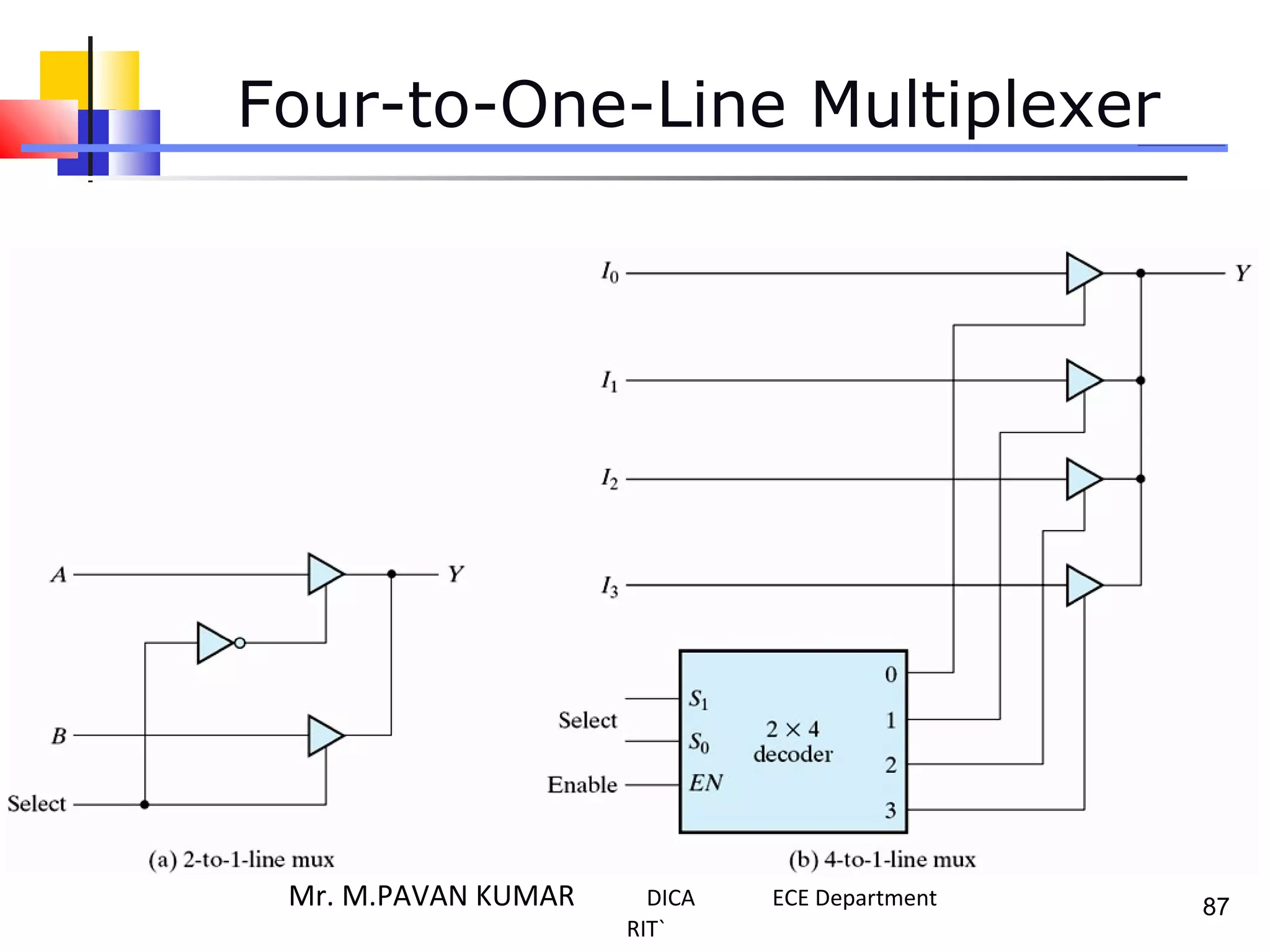


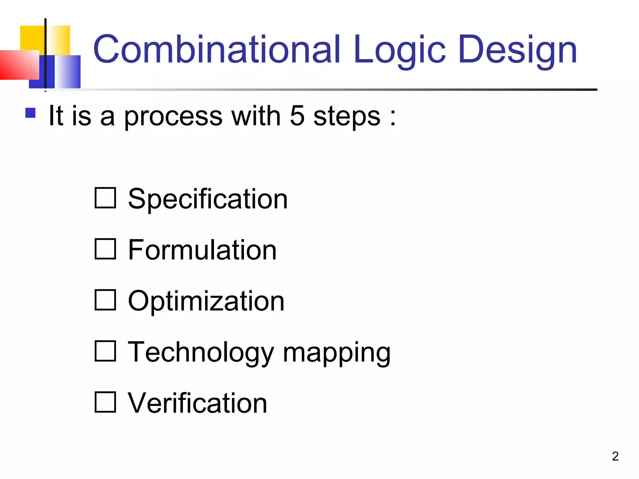
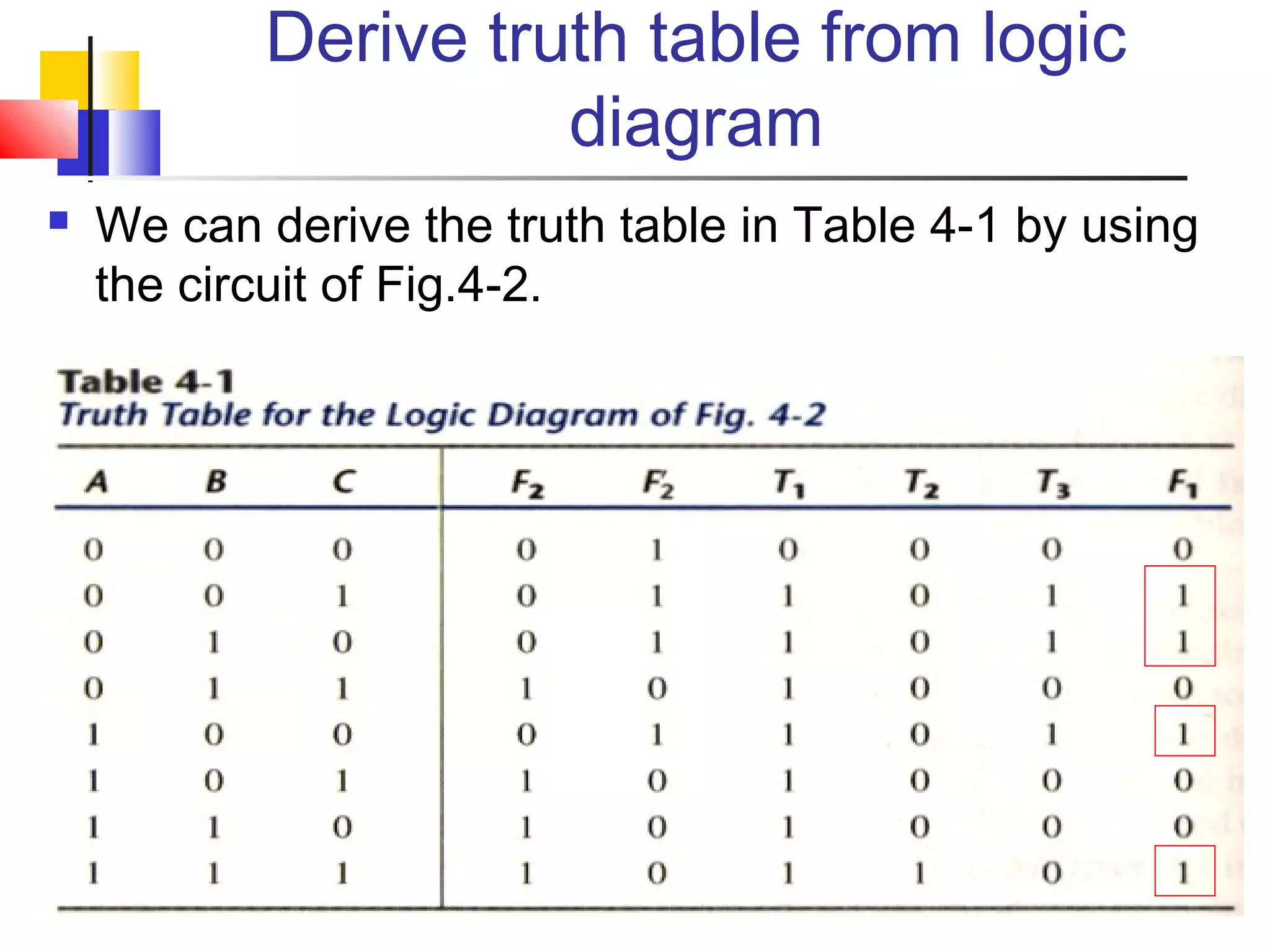
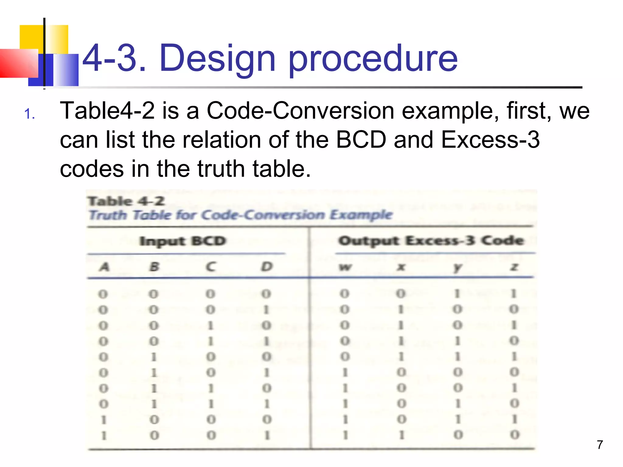
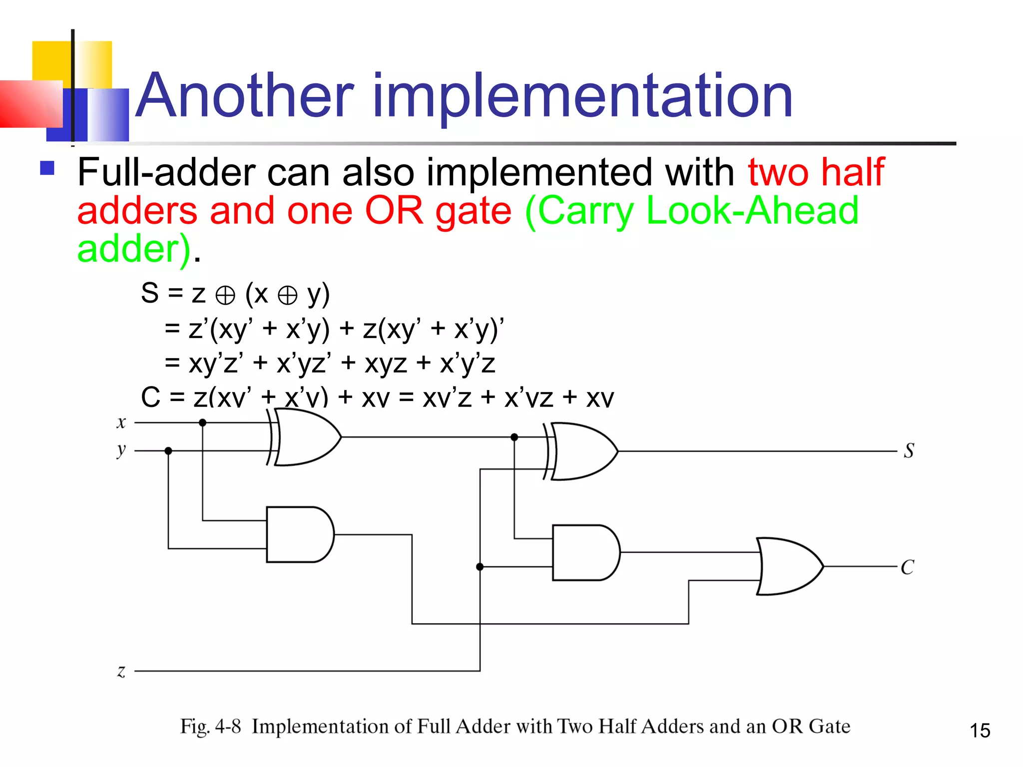
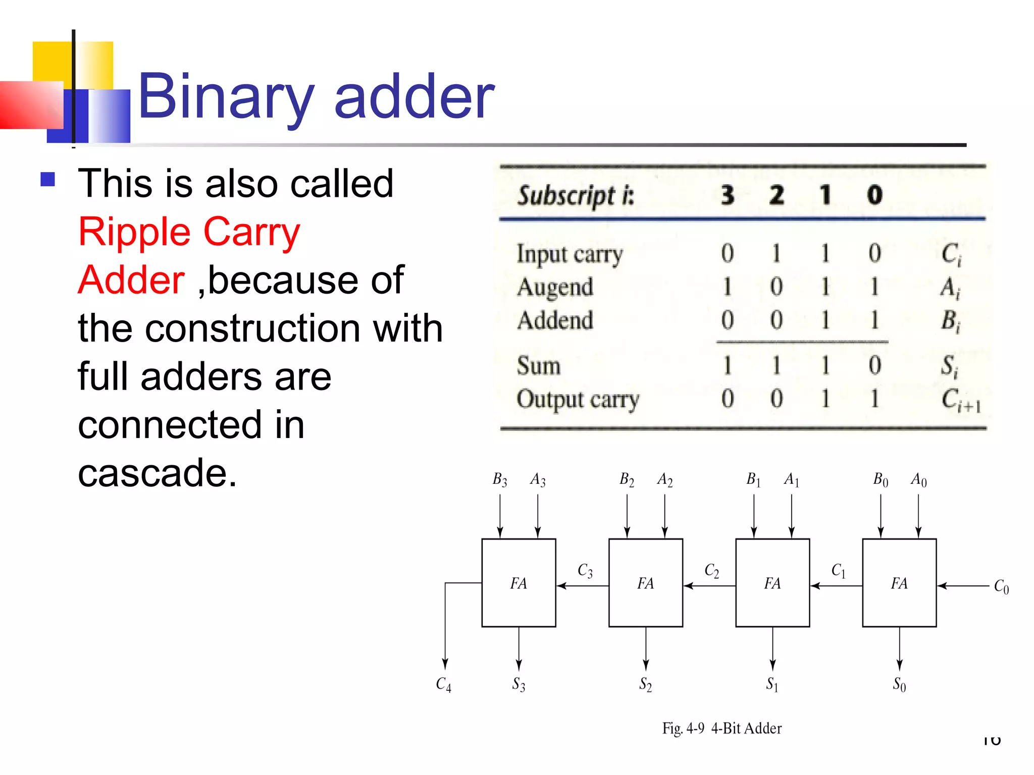
The document discusses combinational logic circuits. It describes combinational logic design procedures including specification, formulation, optimization, technology mapping, and verification. It also discusses analysis procedures for logic diagrams, including labeling gate outputs and determining Boolean functions. Additional topics covered include half adders, full adders, binary adders, decoders, encoders, multiplexers, priority encoders, and binary-coded decimal to seven-segment displays. Diagrams and truth tables are provided for various logic gates and circuits.