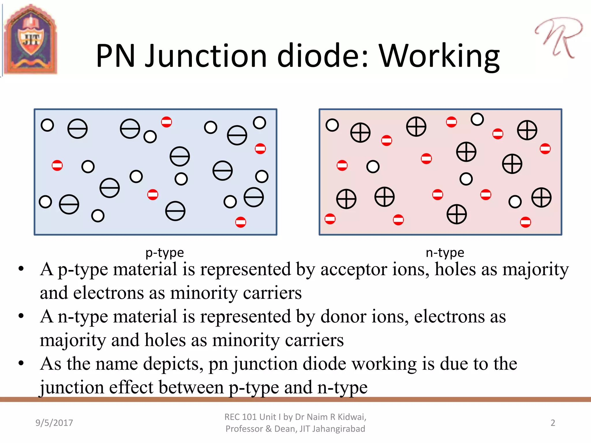
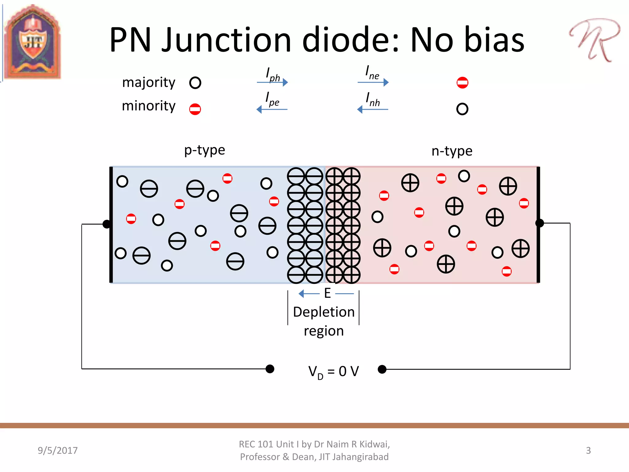
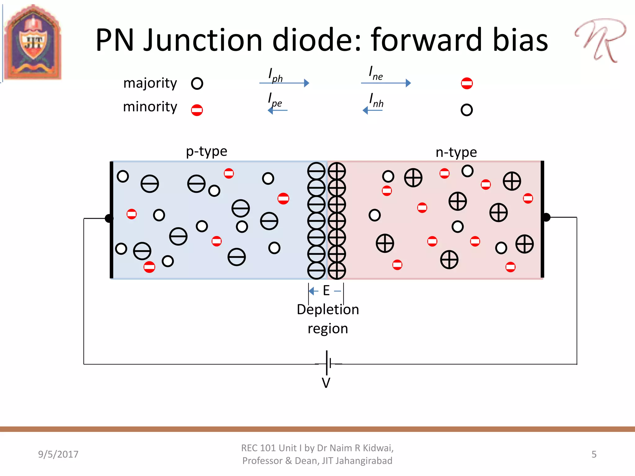
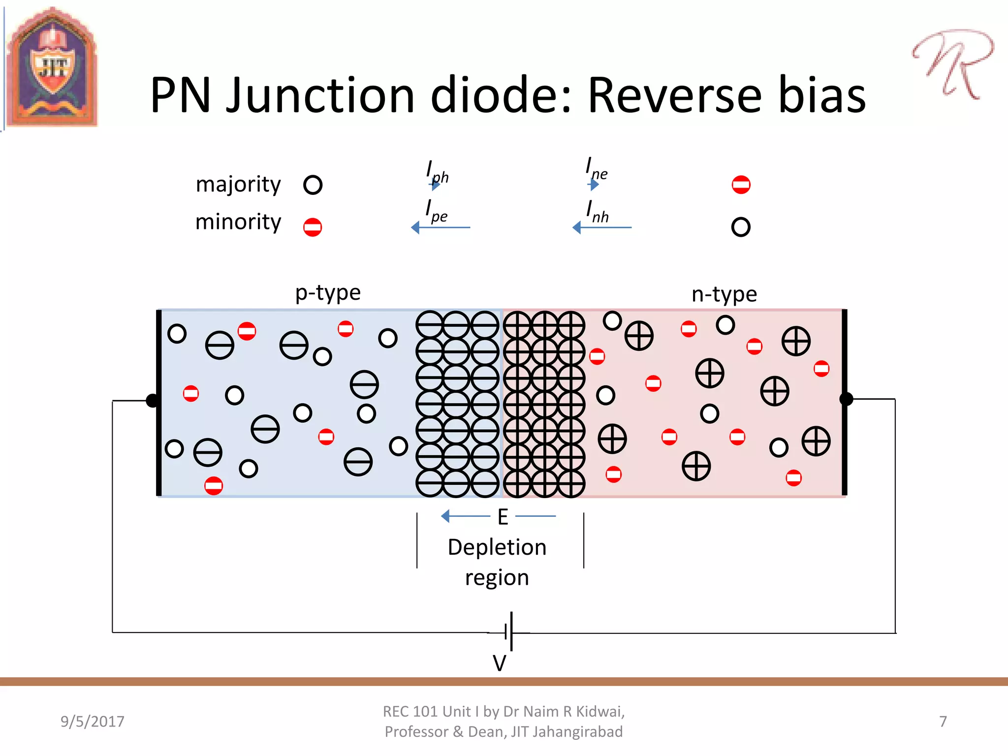
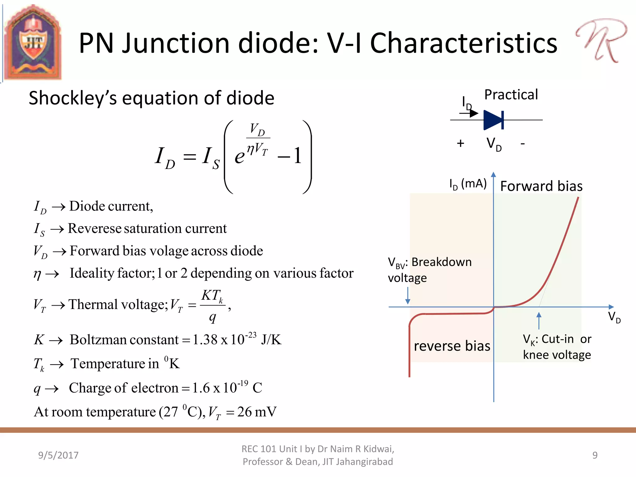
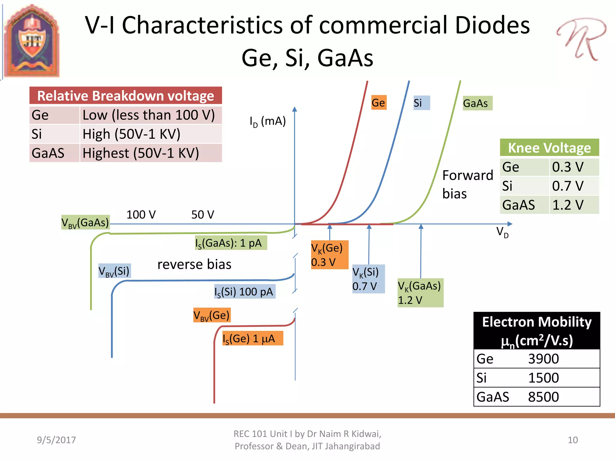
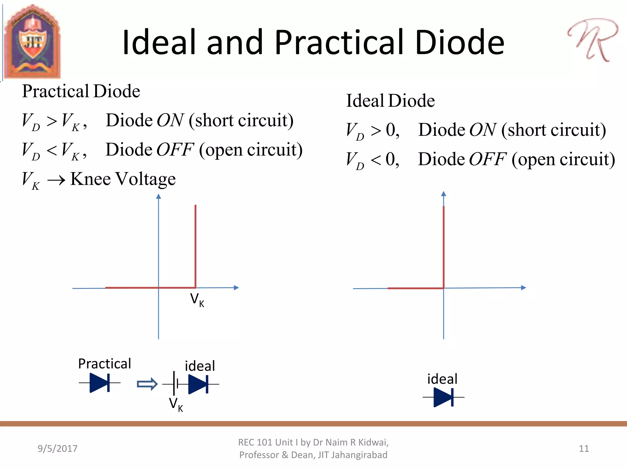
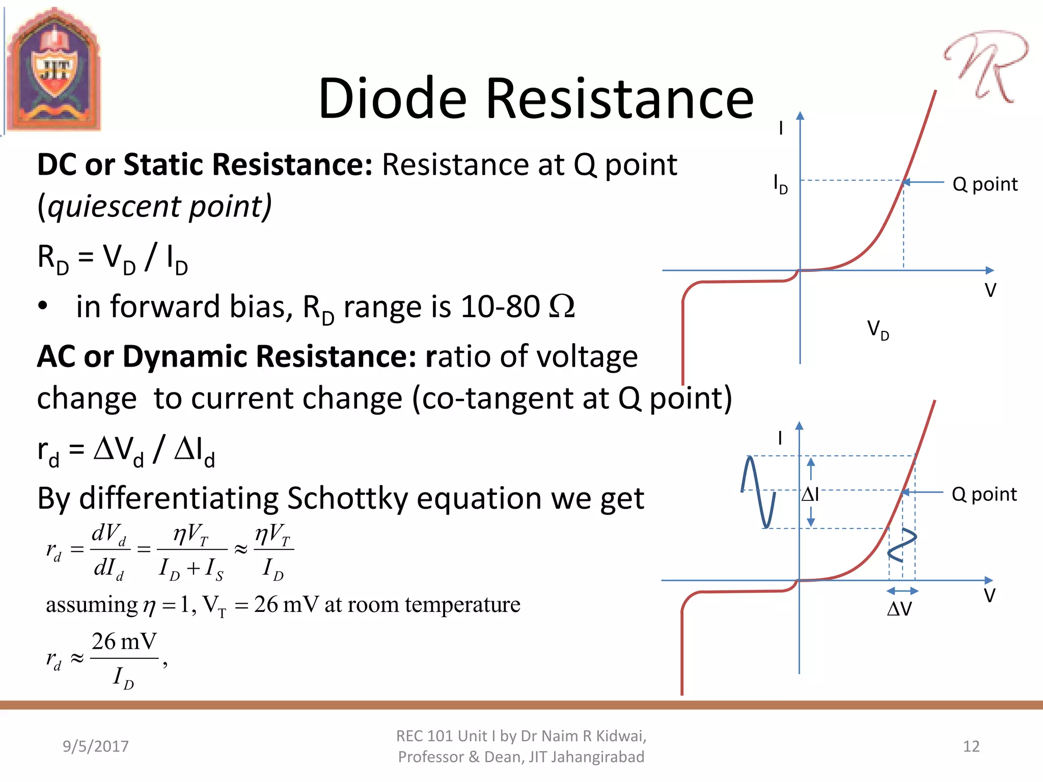
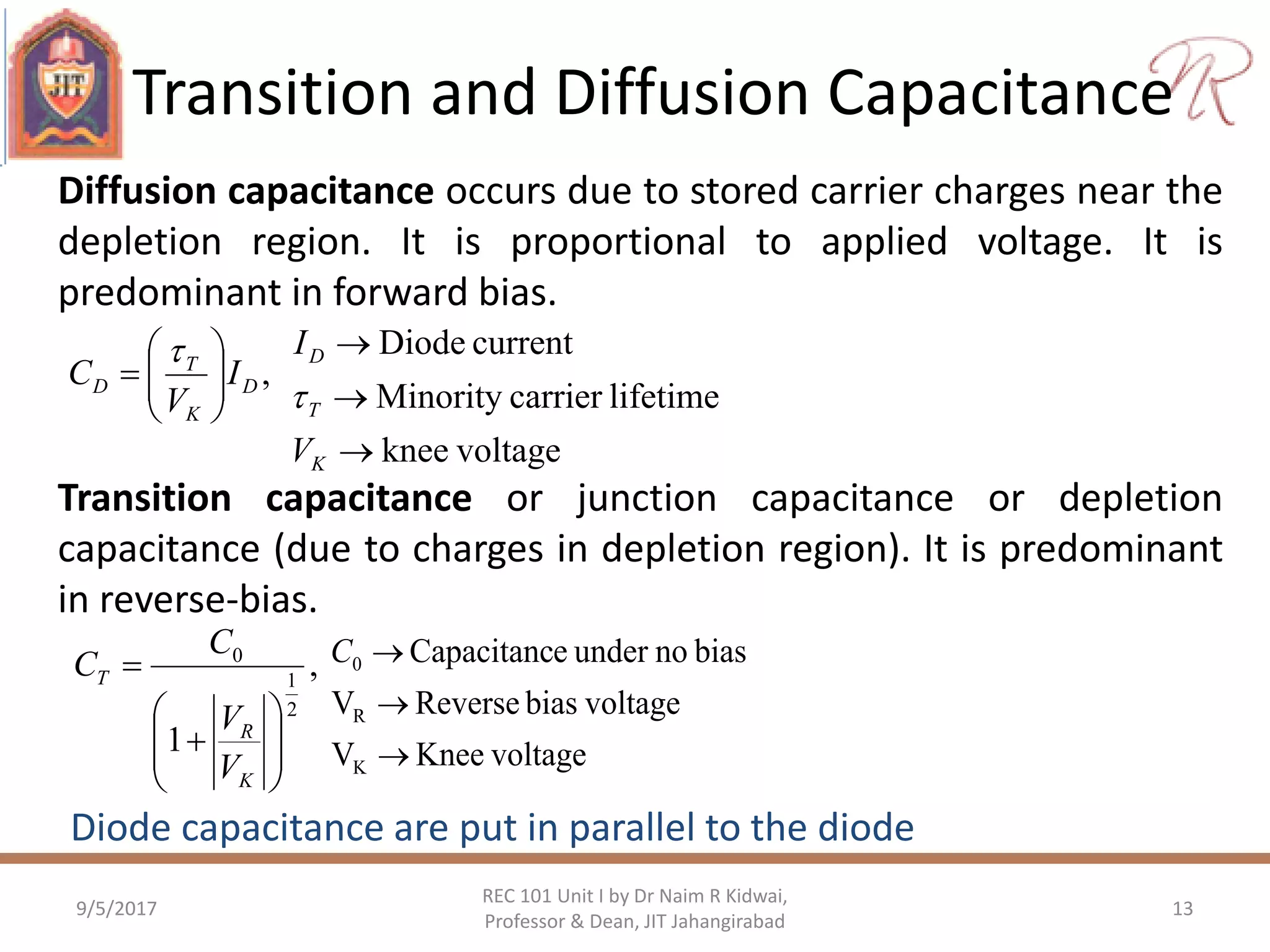
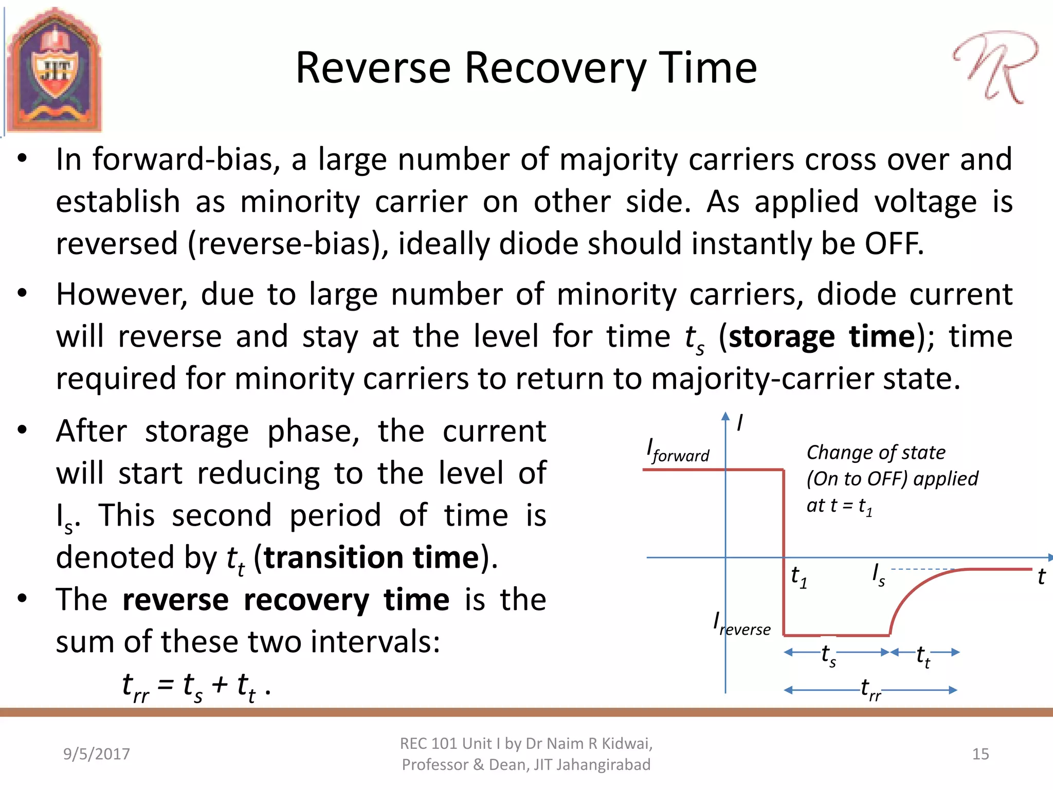
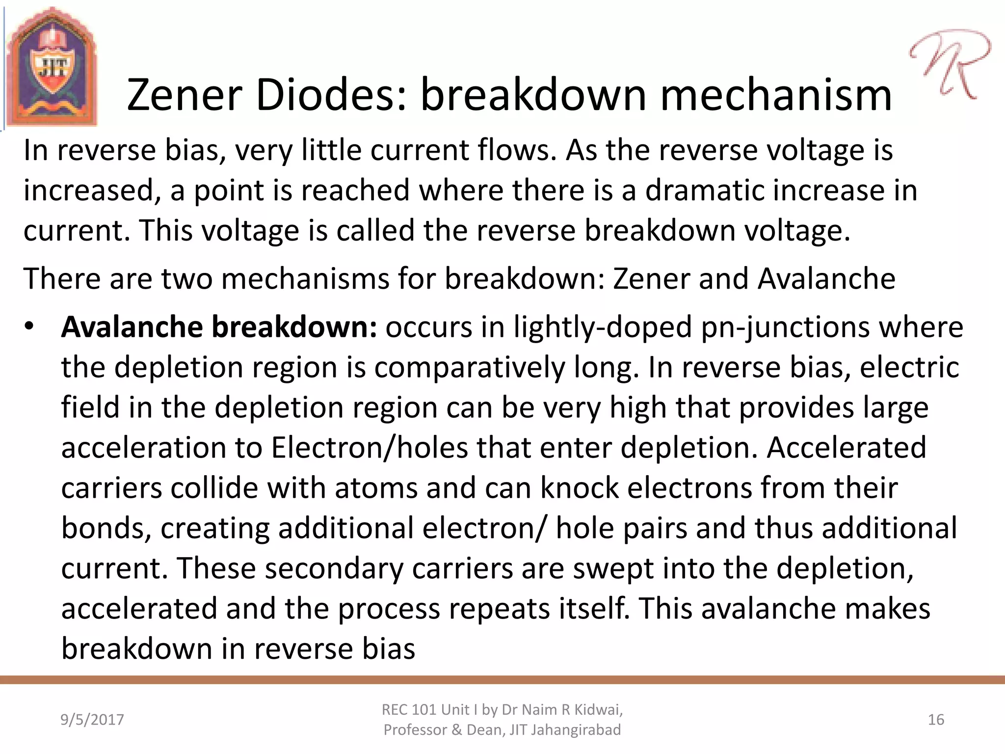
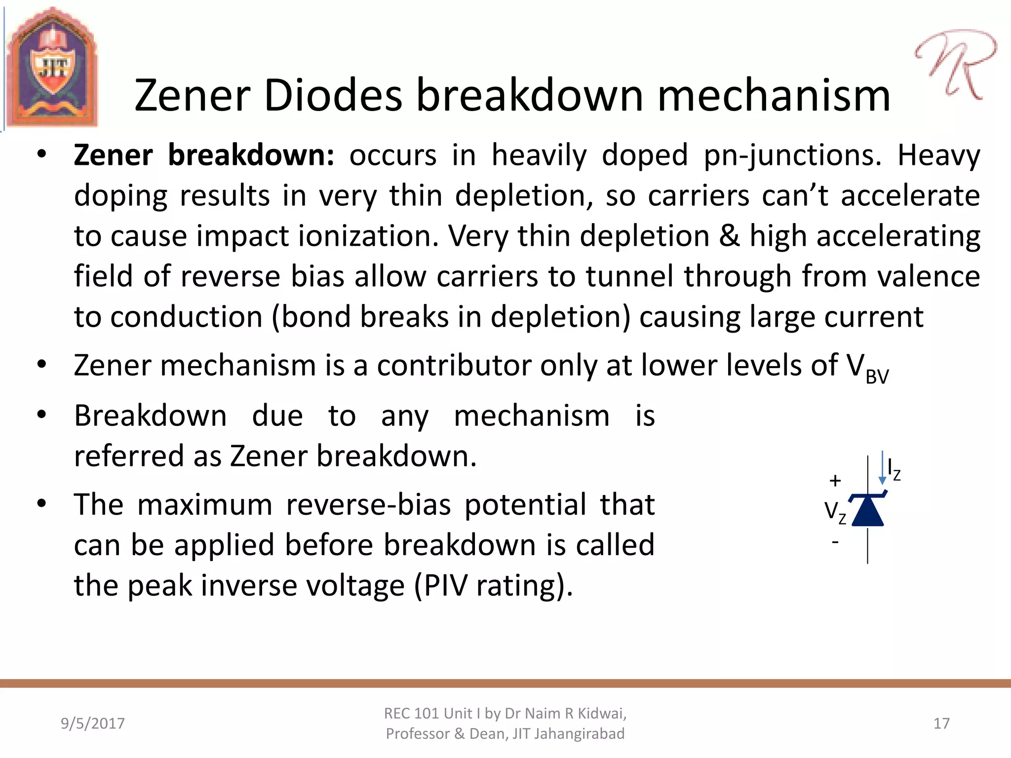
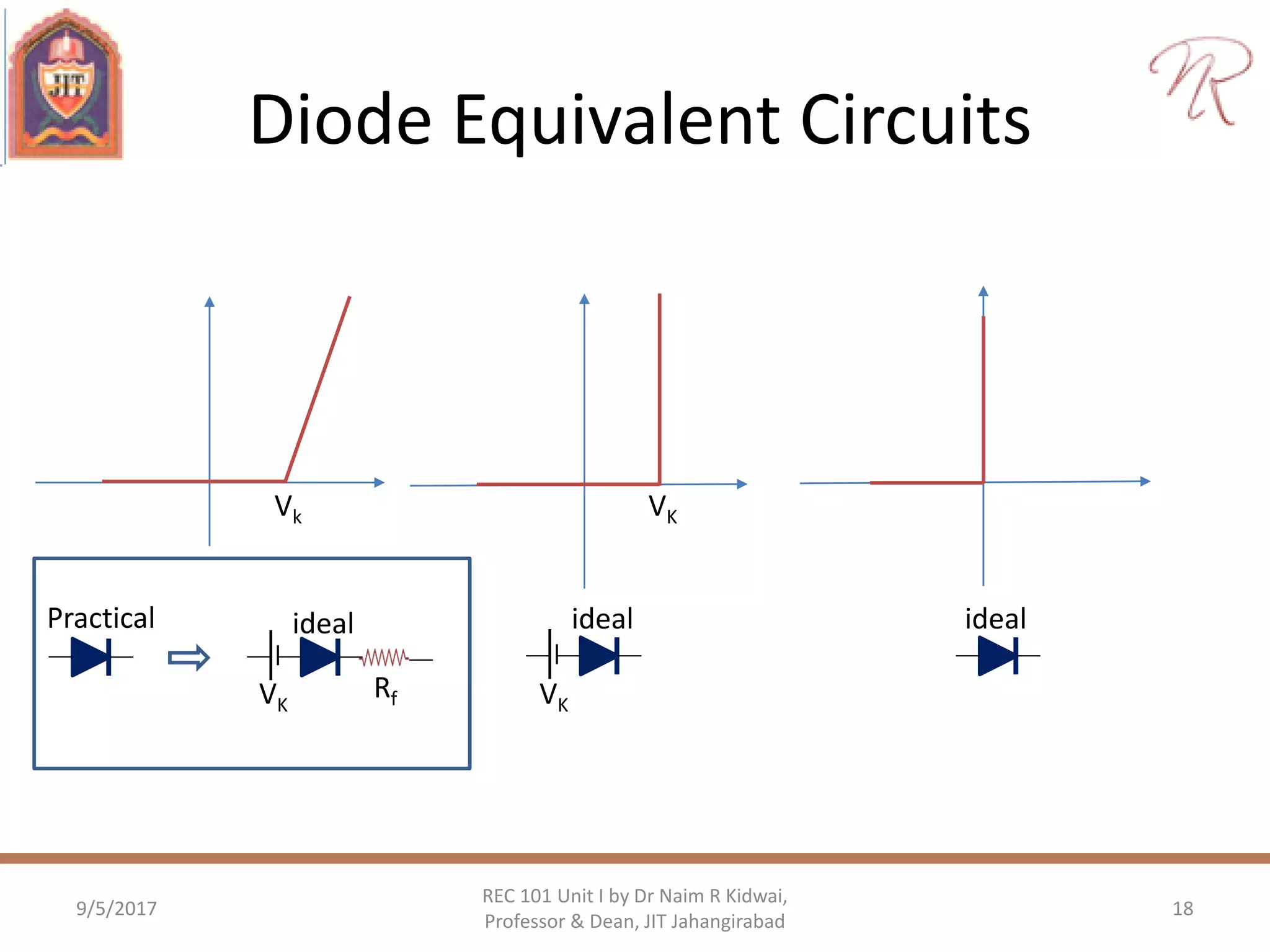
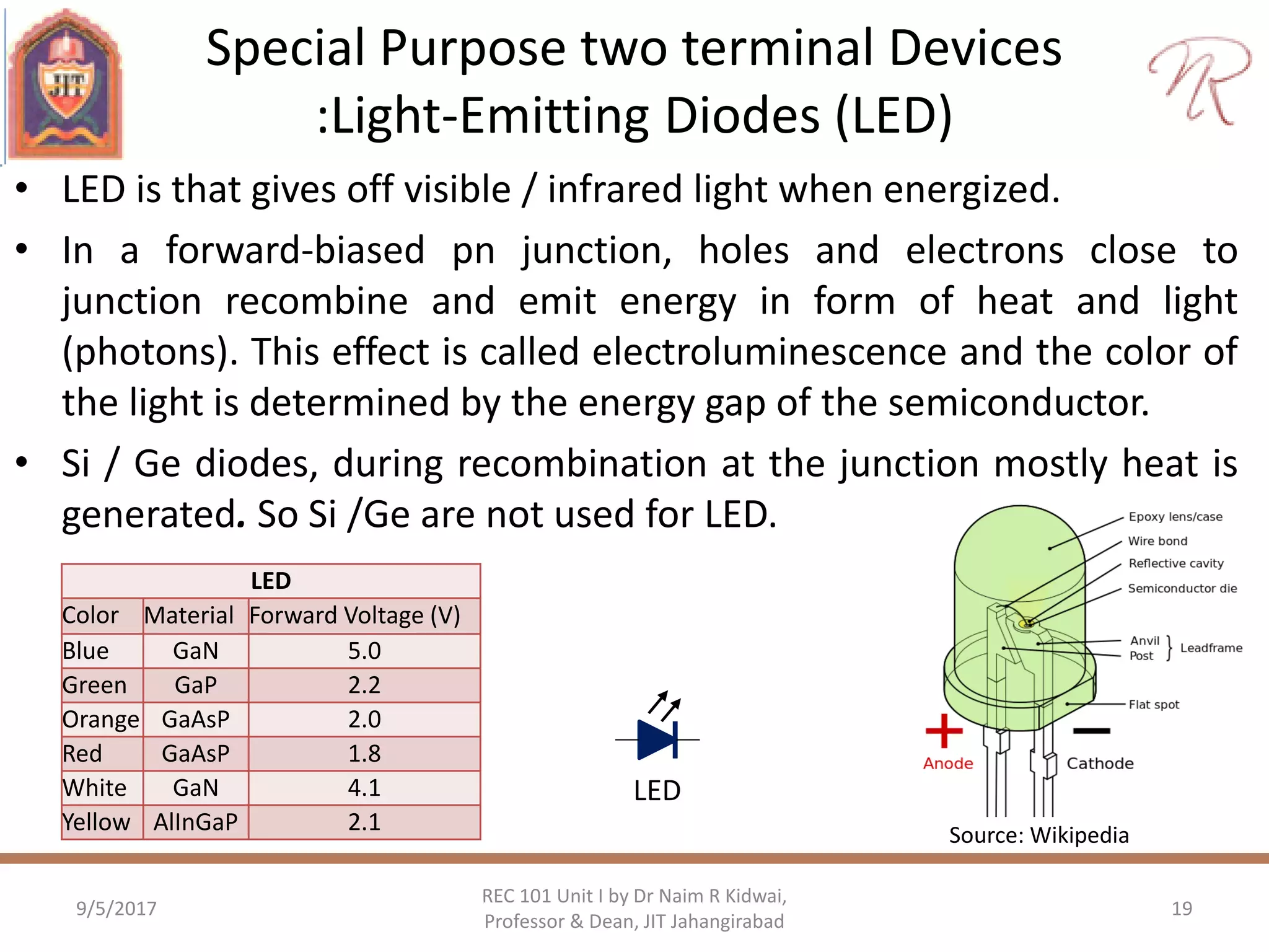
The presentation explains working of pn junction diode, V-I characteristics, breakdown mechanism, ac and dc resistance, diode capacitance, effect of temperature and equivalent circuit. It also covers special diodes, LED, Varicap diodes, Tunnel diode, and working of LCD
Call Girls Service Nagpur Tanvi Call 7001035870 Meet With Nagpur Escorts
Rec101 unit 1 (part ii) pn junction diode
1. PN junction diode
REC 101: Basic Electronics Unit 1
PN junction diode: Introduction of Semiconductor Materials Semiconductor Diode: Depletion
layer, V-I characteristics, ideal and practical, diode resistance, capacitance, Diode Equivalent
Circuits, Transition and Diffusion Capacitance, Zener Diodes breakdown mechanism (Zener
and avalanche) Diode Application: Series , Parallel and Series, Parallel Diode Configuration,
Half and Full Wave rectification, Clippers, Clampers, Zener diode as shunt regulator, Voltage-
Multiplier Circuits Special Purpose two terminal Devices :Light-Emitting Diodes, Varactor
(Varicap) Diodes, Tunnel Diodes, Liquid-Crystal Displays.
9/5/2017 1
REC 101 Unit I by Dr Naim R Kidwai,
Professor & Dean, JIT Jahangirabad
2. PN Junction diode: Working
9/5/2017 2
REC 101 Unit I by Dr Naim R Kidwai,
Professor & Dean, JIT Jahangirabad
p-type n-type
• A p-type material is represented by acceptor ions, holes as majority
and electrons as minority carriers
• A n-type material is represented by donor ions, electrons as
majority and holes as minority carriers
• As the name depicts, pn junction diode working is due to the
junction effect between p-type and n-type
3. PN Junction diode: No bias
9/5/2017 3
REC 101 Unit I by Dr Naim R Kidwai,
Professor & Dean, JIT Jahangirabad
VD = 0 V
Depletion
region
E
Iph
Ine
majority
minority
InhIpe
n-typep-type
4. PN Junction diode: No bias
9/5/2017 4
REC 101 Unit I by Dr Naim R Kidwai,
Professor & Dean, JIT Jahangirabad
• As the p-type and n-type are “joined”, the electrons & holes diffuses
across the junction and combine, resulting in a region with +ve charge
in n-region and –ve charge in p-region thus forming a barrier potential.
• This action continues until the barrier potential repels further diffusion
• In the region near junction only donor and acceptor atoms remain
• The region of positive and negative ions is called the depletion region
due to the “depletion” of free carriers in the region.
• In depletion region, Electric field (from +ve to –ve ions) oppose
majority carrier crossover and facilitate minority carrier crossover.
• At equilibrium number of majority carrier crossing the junction is
equal to number of minority carriers, thus no current flows (Direction
of minority current component is opposite to majority carrier current
component)
5. PN Junction diode: forward bias
9/5/2017 5
REC 101 Unit I by Dr Naim R Kidwai,
Professor & Dean, JIT Jahangirabad
Depletion
region
E
majority
minority
InhIpe
Iph
Ine
n-typep-type
V
6. PN Junction diode: forward bias
9/5/2017 6
REC 101 Unit I by Dr Naim R Kidwai,
Professor & Dean, JIT Jahangirabad
• A forward-bias or “on” condition is made by applying the
forward bias potential (+ve potential to the p -type and the -ve
potential to the n -type material)
• Forward-bias potential will “pressure” electrons in the n -type
and holes in the p-type material to recombine with the ions near
the boundary and reduce the width of the depletion region.
• The minority-carrier flow does change in magnitude, but the
reduction in the width of the depletion region results in a heavy
majority flow across the junction.
• As the forward bias increases in magnitude, the depletion region
will continue to decrease in width until a flood of electrons can
pass through the junction, resulting in an exponential rise in
current as shown in forward-bias region of the characteristics
7. PN Junction diode: Reverse bias
9/5/2017 7
REC 101 Unit I by Dr Naim R Kidwai,
Professor & Dean, JIT Jahangirabad
Depletion
region
E
majority
minority
InhIpe
Iph
Ine
n-typep-type
V
8. PN Junction diode: Reverse bias
9/5/2017 8
REC 101 Unit I by Dr Naim R Kidwai,
Professor & Dean, JIT Jahangirabad
• A reverse-bias or “off” condition is made by applying the reverse
bias potential (-ve potential to p -type and +ve potential to the n -
type material)
• Reverse-bias potential will result in widening of width of the
depletion region.
• The minority-carrier flow does change in magnitude, but the
widening of the depletion region results in great increase of
potential barrier to majority carrier flow across the junction to the
point that majority carrier flow across the junction stops.
• The current that exists under reverse-bias is called the reverse
saturation current (only due to minority carriers)
• As reverse bias increases, the depletion region will continue to
widen until a breakdown occurs.
9. PN Junction diode: V-I Characteristics
9/5/2017 9
REC 101 Unit I by Dr Naim R Kidwai,
Professor & Dean, JIT Jahangirabad
Forward bias
reverse bias VK: Cut-in or
knee voltage
VD
ID (mA)
VBV: Breakdown
voltage
Practical
+ VD -
ID
1T
D
V
V
SD eII
mV26C),(27retemperaturoomAt
C10x1.6electronofCharge
KineTemperatur
J/K10x1.38constantBoltzman
,voltage;Thermal
factoron variousdepending2or1factor;Ideality
diodeacrossvolagebiasForward
currentsaturationReverese
current,Diode
0
19-
0
23-
T
k
k
TT
D
S
D
V
q
T
K
q
KT
VV
V
I
I
Shockley’s equation of diode
10. V-I Characteristics of commercial Diodes
Ge, Si, GaAs
9/5/2017 10
REC 101 Unit I by Dr Naim R Kidwai,
Professor & Dean, JIT Jahangirabad
Forward
bias
reverse bias
VK(Ge)
0.3 V
VD
ID (mA)
VK(GaAs)
1.2 V
VK(Si)
0.7 V
GaAsSiGe
IS(Ge) 1 A
IS(GaAs): 1 pA
IS(Si) 100 pA
VBV(GaAs)
VBV(Si)
VBV(Ge)
50 V100 V
Knee Voltage
Ge 0.3 V
Si 0.7 V
GaAS 1.2 V
Relative Breakdown voltage
Ge Low (less than 100 V)
Si High (50V-1 KV)
GaAS Highest (50V-1 KV)
Electron Mobility
n(cm2/V.s)
Ge 3900
Si 1500
GaAS 8500
11. Ideal and Practical Diode
9/5/2017 11
REC 101 Unit I by Dr Naim R Kidwai,
Professor & Dean, JIT Jahangirabad
Practical
ideal
VK
VK
ideal
circuit)(openDiode,0
circuit)(shortDiode,0
DiodeIdeal
OFFV
ONV
D
D
VoltageKnee
circuit)(openDiode,
circuit)(shortDiode,
DiodePractical
K
KD
KD
V
OFFVV
ONVV
12. Diode Resistance
DC or Static Resistance: Resistance at Q point
(quiescent point)
RD = VD / ID
• in forward bias, RD range is 10-80
AC or Dynamic Resistance: ratio of voltage
change to current change (co-tangent at Q point)
rd = Vd / Id
By differentiating Schottky equation we get
9/5/2017
REC 101 Unit I by Dr Naim R Kidwai,
Professor & Dean, JIT Jahangirabad
12
V
I
V
I Q point
V
I
ID Q point
VD
,
mV26
retemperaturoomatmV26V1,assuming T
D
d
D
T
SD
T
d
d
d
I
r
I
V
II
V
dI
dV
r
13. Transition and Diffusion Capacitance
Diffusion capacitance occurs due to stored carrier charges near the
depletion region. It is proportional to applied voltage. It is
predominant in forward bias.
9/5/2017
REC 101 Unit I by Dr Naim R Kidwai,
Professor & Dean, JIT Jahangirabad
13
Transition capacitance or junction capacitance or depletion
capacitance (due to charges in depletion region). It is predominant
in reverse-bias.
,
1
2
1
0
K
R
T
V
V
C
C
voltageKneeV
voltagebiasReverseV
biasnoundereCapacitanc
K
R
0
C
,D
K
T
D I
V
C
voltageknee
lifetimecarrierMinority
currentDiode
K
T
D
V
I
Diode capacitance are put in parallel to the diode
14. Effect of Temperature on pn junction diode
Increase of temperature results in increase in carrier concentration.
As a result , Knee voltage and reverse breakdown voltage decreases
while Reverse saturation current increases
• In the forward-bias region the characteristics of a silicon diode
shift to the left at a rate of 2.5 mV per centigrade degree increase
in temperature
• In the reverse-bias region the reverse current of a silicon diode
doubles for every 10°C rise in temperature
9/5/2017
REC 101 Unit I by Dr Naim R Kidwai,
Professor & Dean, JIT Jahangirabad
14
15. Reverse Recovery Time
• In forward-bias, a large number of majority carriers cross over and
establish as minority carrier on other side. As applied voltage is
reversed (reverse-bias), ideally diode should instantly be OFF.
• However, due to large number of minority carriers, diode current
will reverse and stay at the level for time ts (storage time); time
required for minority carriers to return to majority-carrier state.
9/5/2017
REC 101 Unit I by Dr Naim R Kidwai,
Professor & Dean, JIT Jahangirabad
15
• After storage phase, the current
will start reducing to the level of
Is. This second period of time is
denoted by tt (transition time).
• The reverse recovery time is the
sum of these two intervals:
trr = ts + tt . trr
ts tt
Is
Iforward
Ireverse
t1
I
t
Change of state
(On to OFF) applied
at t = t1
16. Zener Diodes: breakdown mechanism
In reverse bias, very little current flows. As the reverse voltage is
increased, a point is reached where there is a dramatic increase in
current. This voltage is called the reverse breakdown voltage.
There are two mechanisms for breakdown: Zener and Avalanche
• Avalanche breakdown: occurs in lightly-doped pn-junctions where
the depletion region is comparatively long. In reverse bias, electric
field in the depletion region can be very high that provides large
acceleration to Electron/holes that enter depletion. Accelerated
carriers collide with atoms and can knock electrons from their
bonds, creating additional electron/ hole pairs and thus additional
current. These secondary carriers are swept into the depletion,
accelerated and the process repeats itself. This avalanche makes
breakdown in reverse bias
9/5/2017
REC 101 Unit I by Dr Naim R Kidwai,
Professor & Dean, JIT Jahangirabad
16
17. Zener Diodes breakdown mechanism
• Zener breakdown: occurs in heavily doped pn-junctions. Heavy
doping results in very thin depletion, so carriers can’t accelerate
to cause impact ionization. Very thin depletion & high accelerating
field of reverse bias allow carriers to tunnel through from valence
to conduction (bond breaks in depletion) causing large current
• Zener mechanism is a contributor only at lower levels of VBV
9/5/2017
REC 101 Unit I by Dr Naim R Kidwai,
Professor & Dean, JIT Jahangirabad
17
• Breakdown due to any mechanism is
referred as Zener breakdown.
• The maximum reverse-bias potential that
can be applied before breakdown is called
the peak inverse voltage (PIV rating).
+
VZ
-
IZ
18. Diode Equivalent Circuits
9/5/2017 18
REC 101 Unit I by Dr Naim R Kidwai,
Professor & Dean, JIT Jahangirabad
Vk VK
Practical ideal
VK
idealideal
VK
Rf
19. Special Purpose two terminal Devices
:Light-Emitting Diodes (LED)
• LED is that gives off visible / infrared light when energized.
• In a forward-biased pn junction, holes and electrons close to
junction recombine and emit energy in form of heat and light
(photons). This effect is called electroluminescence and the color of
the light is determined by the energy gap of the semiconductor.
• Si / Ge diodes, during recombination at the junction mostly heat is
generated. So Si /Ge are not used for LED.
9/5/2017
REC 101 Unit I by Dr Naim R Kidwai,
Professor & Dean, JIT Jahangirabad
19
LED
Color Material Forward Voltage (V)
Blue GaN 5.0
Green GaP 2.2
Orange GaAsP 2.0
Red GaAsP 1.8
White GaN 4.1
Yellow AlInGaP 2.1
LED
Source: Wikipedia
20. Special Purpose two terminal Devices
:Light-Emitting Diodes (LED)
• GaAs diodes emit light in the infrared zone while GaAsP, GaN diodes
emit light in visible region.
• The frequency for infrared light extends from about 100-400 THz,
with the visible light spectrum extending from about 400-750 THz.
• LED efficacy is, given as ratio of lumens generated per applied
electrical power (watt)
• A major concern of LED is Low breakdown voltage (typically 3-5 V)
• Earlier only green/yellow/orange/red LED were available (VF=2V)
• In 1990’s blue LED (VF=5 V ) and white LED (VF=4.1 V ) introduced
• Now LED efficacy is 100-135 lumens /watt
• LED find applications in display devices and home lighting
9/5/2017
REC 101 Unit I by Dr Naim R Kidwai,
Professor & Dean, JIT Jahangirabad
20
21. Special Purpose two terminal Devices :
Varactor (Varicap) Diodes,
• A varactor (varicap) diode/ tuning diode/ variable capacitance
diode/ variable reactance diode, has a variable capacitance which
is a function of the voltage that is impressed on its terminals.
• Varactor diodes are operated in reverse-bias, so no current flows.
However, as thickness of the depletion varies with the applied
bias voltage, the capacitance of the diode varies.
• Capacitance is inversely proportional to the depletion thickness
which in turn is proportional to the square root of the voltage.
9/5/2017
REC 101 Unit I by Dr Naim R Kidwai,
Professor & Dean, JIT Jahangirabad
21
Varicap
,
1
2
1
0
K
R
T
V
V
C
C
22. Special Purpose two terminal Devices :
Tunnel Diodes
• Tunnel diode (Esaki diode named after discoverer) is a highly
doped semiconductor device and is used mainly for low voltage
high frequency switching applications. It works on the principle of
Tunnelling effect.
• Tunnel diode is about 1000 times more heavily doped than
normal diode
• Its depletion region is very thin (0.0001 mm)
• Tunnel diode has special characteristics of negative resistance
• Tunnel diodes are used in high speed applications and oscillators.
• Heavy doping reduce Zener breakdown voltage to very low value.
9/5/2017
REC 101 Unit I by Dr Naim R Kidwai,
Professor & Dean, JIT Jahangirabad
22
23. Special Purpose two terminal Devices :
Tunnel Diodes
9/5/2017
REC 101 Unit I by Dr Naim R Kidwai,
Professor & Dean, JIT Jahangirabad
23
VD
ID
Ip
Iv
Vp Vv
-ve resistance zone
Peak
Valley
• As per quantum mechanics
there exists non zero
probability that the particle
with energy less than the
energy barrier will cross the
barrier as if it tunnels across
the barrier. This is called
as Tunnelling effect. The
probability increases with the
decreasing barrier energy.
Tunnel
24. Special Purpose two terminal Devices :
Liquid-Crystal Displays.
• LCD has the advantage of having a lower power requirement than
the LED, typically in W , compared to the mW for LEDs.
• It does, require an external or internal light source, and is limited
to a temperature range of about 0°C to 60°C.
• Lifetime is an area of concern as LCDs can chemically degrade.
• Types of LCD unit are field-effect and dynamic-scattering units.
• A liquid crystal is a material that flows like a liquid but whose
molecular structure has some properties normally associated with
solids. For light scattering units, the greatest interest is in nematic
liquid crystal, which has the rodlike crystal structure
• It passes the light, but when voltage is applied, molecular
structure is disturbed, resulting in regions with different
reflections
9/5/2017
REC 101 Unit I by Dr Naim R Kidwai,
Professor & Dean, JIT Jahangirabad
24
25. Special Purpose two terminal Devices :
Liquid-Crystal Displays.
9/5/2017
REC 101 Unit I by Dr Naim R Kidwai,
Professor & Dean, JIT Jahangirabad
25
Glass
Glass
Sealer
V=0
Incident light
Glass
Glass
Sealer
+
V
-
Incident light
Clear region Frosted region
Iridum oxide surface with
Conductive clear coating
Nematic Liquid crystal with no bias Nematic Liquid crystal with applied bias
26. Special Purpose two terminal Devices :
Liquid-Crystal Displays.
9/5/2017
REC 101 Unit I by Dr Naim R Kidwai,
Professor & Dean, JIT Jahangirabad
26
• The field-effect or twisted nematic LCD has the same segmented
appearance and thin layer of encapsulated liquid crystal, but its
mode of operation is very different.
• Similar to dynamic-scattering LCD, the field-effect LCD can be
operated in reflective or transmissive mode with an internal source.
• The internal light source is on the right, and the viewer is on the
left. It has an an addition of a light polarizer .
• Only the vertical component of the entering light on the right can
pass through the vertical-light polarizer on the right.
• In field-effect LCD, either the clear conducting surface to the right is
chemically etched or organic film is applied to orient the molecules
in the liquid crystal in the vertical plane, parallel to cell wall.
27. Special Purpose two terminal Devices :
Liquid-Crystal Displays.
9/5/2017
REC 101 Unit I by Dr Naim R Kidwai,
Professor & Dean, JIT Jahangirabad
27
Glass
Glass
Sealer +
V
-
Incident light
clear Conductive surface
Vertical
light
polarizers