Download as PDF, PPTX
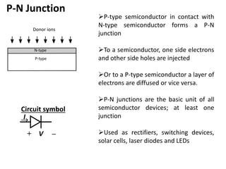
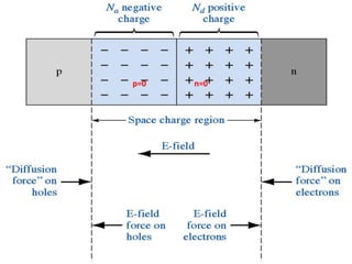
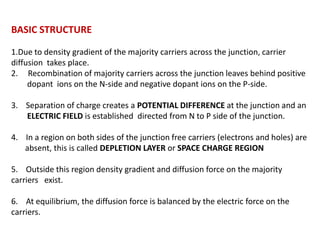
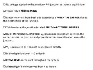
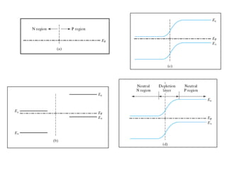
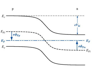
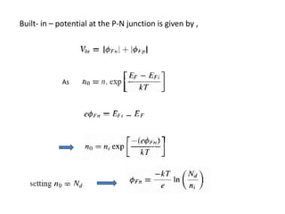
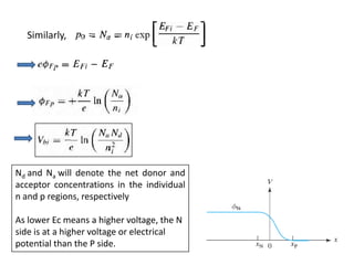
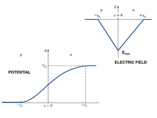
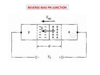
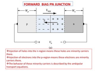
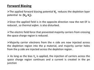
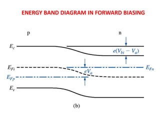
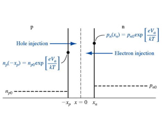
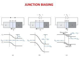

The document discusses P-N junctions, which are formed at the interface between P-type and N-type semiconductors. When these materials come into contact, majority charge carriers diffuse across the junction, leaving behind charged dopant ions. This creates an electric field and depletion region across the junction. At equilibrium with no applied voltage, a built-in potential barrier forms that prevents further carrier recombination. P-N junctions can be forward or reverse biased by an external voltage, affecting the electric field and current flow. They are the basic components of many semiconductor devices such as diodes, transistors, and solar cells.