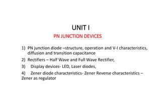
SlideShare a Scribd company logo
UNIT I
PN JUNCTION DEVICES
1) PN junction diode –structure, operation and V-I characteristics,
diffusion and transition capacitance
2) Rectifiers – Half Wave and Full Wave Rectifier,
3) Display devices- LED, Laser diodes,
4) Zener diode characteristics- Zener Reverse characteristics –
Zener as regulator
Types of Diodes
PN junction diode
• If we take P type semiconductor or N type semi conductor separately,
it is of little use
• If we join a piece of P type material with an N type material such that
crystal structure remains continuous at the boundary, a PN junction is
formed
• The p-n junction diode is made from the semiconductor materials
such as silicon, germanium, and gallium arsenide.
• The p-n junction diodes made from silicon semiconductors works at
higher temperature when compared with the p-n junction diodes
made from germanium semiconductors. Hence silicon is more
preferred
PN Diode
Formation of PN Junction
• Joining n-type material with p-type material causes excess electrons
in the n-type material to diffuse to the p-type side and excess holes
from the p-type material to diffuse to the n-type side.
• Movement of electrons to the p-type side exposes positive ions in the
n-type side while movement of holes to the n-type side exposes
negative ions in the p-type side, resulting in an electron field at the
junction and forming the depletion region.
• A voltage results from the electric field formed at the junction.
Operation of Diode
• The n side will have large number of electrons and very few holes (due to thermal
excitation) whereas the p side will have high concentration of holes and very few
electrons. Due to this a process called diffusion takes place. In this process free
electrons from the n side will diffuse (spread) into the p side and combine with
holes present there, leaving a positive immobile (not moveable) ion in the n side.
Hence few atoms on the p side are converted into negative ions.
• Similarly few atoms on the n-side will get converted to positive ions.
• Due to this large number of positive ions and negative ions will accumulate on
the n-side and p-side respectively. This region so formed is called as depletion
region.
• Due to the presence of these positive and negative ions a static electric
field called as "barrier potential" is created across the p-n junction of the diode. It
is called as "barrier potential" because it acts as a barrier and opposes the flow of
positive and negative ions across the junction.
Biasing of Diode
• Applying an external DC voltage to the diode is called
as biasing.
• If the p-side (anode) is connected to the positive
terminal of the supply and the n-side (cathode) to the
negative terminal of the supply, the diode is said to be
forward biased.
• If the n-side is connected to the positive terminal of
the supply and the p-side to the negative terminal of
the supply, the diode is said to be reversed biased.
Types of Biasing
Zero Biased PN Junction Diode
1)No external energy source is applied
2)A natural Potential Barrier is developed across a depletion layer which is
approximately 0.5 to 0.7v for silicon diodes and approximately 0.3 of a volt
for germanium diodes.
Reverse Biased PN Junction Diode
1)thickness of the depletion region increases
2)the diode acts like an open circuit blocking any current flow,
(only a very small leakage current).
Forward Biased PN Junction Diode
1)The thickness of the depletion region reduces
2)The diode acts like a short circuit allowing full current
to flow
V-I characteristics of Diode
Diode Current
Diode current equation expresses the relationship between the current flowing through the diode
as a function of the voltage applied across it. Mathematically it is given as
where:
I = the net current flowing through the diode;
I0 = "dark saturation current", the diode leakage current density in the absence
of light;
V = applied voltage across the terminals of the diode;
q = absolute value of electron charge;
k = Boltzmann's constant; and
T = absolute temperature (K)
n= between 1 and 2, ideality factor
.
Diode Current (contd.)
• In forward biased condition, there will a large amount of
current flow through the diode. Thus the diode current
equation (equation 1) becomes
• On the other hand, if the diode is reverse biased, then the
exponential term in equation (1) becomes negligible. Thus we
have
Diode junction capacitances
• Transition capacitance (CT)
• Diffusion capacitance (CD)
Transition Capacitance
1. When P-N junction is reverse biased the depletion region act as an insulator
or as a dielectric medium and the p-type an N-type region have low
resistance and act as the plates.
2. Thus this P-N junction can be considered as a parallel plate capacitor.
3. This junction capacitance is called as space charge capacitance or transition
capacitance and is denoted as CT .
4. Since reverse bias causes the majority charge carriers to move away from
the junction , so the thickness of the depletion region denoted as W
increases with the increase in reverse bias voltage.
Diode Resistances
• Ideal diode-> Forward Bias-Zero resistance, Reverse Bias-
Infinite resistance
• There are four resistances
1. DC or Static resistance
2. AC or Dynamic resistance
3. Average AC resistance
4. Reverse resistance
Resistor Resistance Graph Diode Resistance Graph
Derivation of Dynamic Resistance
𝐼 = 𝐼0 𝑒 ൗ𝑣
𝜂𝑣 𝑇 − 1
𝑑𝐼
𝑑𝑣
=
𝑑
𝑑𝑣
𝐼0 𝑒 ൗ𝑣
𝜂𝑣 𝑇 − 1
=
𝐼0 𝑒 ൗ𝑣
𝜂𝑣 𝑇
𝜂𝑣 𝑇
=
𝐼+𝐼0
𝜂𝑣 𝑇
=
𝐼
𝜂𝑣 𝑇
𝑟𝑓 =
𝑑𝑣
𝑑𝐼
=
𝜂𝑣 𝑇
𝐼
=
26 𝑚𝑉
𝐼
Transition Capacitance
• The amount of capacitance changed with increase in voltage is called transition capacitance.
• The transition capacitance is also known as depletion region capacitance, junction
capacitance or barrier capacitance.
• Transition capacitance is denoted as CT.
• The change of capacitance at the depletion region can be defined as the change in electric
charge per change in voltage.
• CT = dQ / dV Where,
CT = Transition capacitance
dQ = Change in electric charge
dV = Change in voltage
• The transition capacitance can be mathematically written as,
CT = ε A / W Where,
ε = Permittivity of the semiconductor
A = Area of plates or p-type and n-type regions
W = Width of depletion region
Diffusion capacitance (CD)
1. When the junction is forward biased, a capacitance comes into play , that is
known as diffusion capacitance denoted as CD. It is much greater than the
transition capacitance.
2. During forward bias, the potential barrier is reduced. The charge carriers
moves away from the junction and recombine.
3. The density of the charge carriers is high near the junction and reduces or
decays as the distance increases.
4. The change in charge with respect to applied voltage results in capacitance
called as diffusion capacitance.
5. Diffusion capacitance is directly proportional to the electric current or
applied voltage.
Diffusion capacitance (CD) (contd.)
• When the width of depletion region decreases, the diffusion
capacitance increases.
• The formula for diffusion capacitance is CD = τ ID / η VT , where τ is the
mean life time of the charge carrier, ID is the diode current and VT is
the applied forward voltage, and η is generation recombination factor.
• The diffusion capacitance is directly proportional to the diode current.
In forward biased CD >> CT . And thus CT can be neglected.
• The diffusion capacitance value will be in the range of nano farads
(nF) to micro farads (μF).
Example:
• For an asymmetrical silicon diode, let the mean life time of the holes
be 10ns, and 𝜂=1. if the forward current is 0.1mA, determine the
diffusion capacitance
• Ans= 38.5pF
Display devices- LED
Display devices- Laser diodes
• Laser Diode is a semiconductor device similar to a light-emitting
diode (LED).
• It uses p-n junction to emit coherent light in which all the waves are
at the same frequency and phase.
• This coherent light is produced by the laser diode using a process
termed as “Light Amplification by Stimulated Emission of Radiation”,
which is abbreviated as LASER.
• Since a p-n junction is used to produce laser light, this device is
named as a laser diode.
Laser diodes
Laser diodes

More Related Content

What's hot

CMOS Logic
CMOS LogicCMOS Logic
Basic electronics, lecture 1
Basic electronics, lecture 1Basic electronics, lecture 1
Basic electronics, lecture 1
Muhammad Ibrahim
 
Zener Diode Full Presentation
Zener Diode Full Presentation Zener Diode Full Presentation
Zener Diode Full Presentation
Adeel Rasheed
 
Mosfet’s
Mosfet’sMosfet’s
Mosfet’s
Ishwar Bhoge
 
Halfwave and full wave rectificaton
Halfwave and full wave rectificaton Halfwave and full wave rectificaton
Halfwave and full wave rectificaton
University of Karachi
 
Logic families
Logic familiesLogic families
Logic families
SARITHA REDDY
 
Presentation on JFET
Presentation on JFETPresentation on JFET
Presentation on JFET
Md. Ashraf Uddin
 
Semiconductor theory
Semiconductor theorySemiconductor theory
Diode v i characteristic
Diode v i characteristicDiode v i characteristic
Diode v i characteristic
Unsa Shakir
 
Analog Electronics ppt on Transition & diffusion capacitance by Being topper
Analog Electronics  ppt on Transition & diffusion capacitance by Being topperAnalog Electronics  ppt on Transition & diffusion capacitance by Being topper
Analog Electronics ppt on Transition & diffusion capacitance by Being topper
Vipin Kumar
 
Tunnel diode
Tunnel diodeTunnel diode
Tunnel diode
Sheikh Danish
 
05-Breakdown in PN Diode.pptx
05-Breakdown in PN Diode.pptx05-Breakdown in PN Diode.pptx
05-Breakdown in PN Diode.pptx
SVNITHISHSELVAN
 
Types of DIODES Basic electronics by sarmad khosa
Types of DIODES Basic electronics by sarmad khosaTypes of DIODES Basic electronics by sarmad khosa
Types of DIODES Basic electronics by sarmad khosa
Sarmad Baloch
 
OPAMP integrator & differentiator.pptx
OPAMP integrator  & differentiator.pptxOPAMP integrator  & differentiator.pptx
OPAMP integrator & differentiator.pptx
JatinMahato1
 
Active and passive
Active and passiveActive and passive
Active and passive
SUneel Gupta
 
Resonance in series and parallel circuits
Resonance in series and parallel circuitsResonance in series and parallel circuits
Resonance in series and parallel circuits
hardikpanchal424
 
Mosfet
MosfetMosfet
Diodes
Diodes Diodes
EST 130, Transistor Biasing and Amplification.
EST 130, Transistor Biasing and Amplification.EST 130, Transistor Biasing and Amplification.
EST 130, Transistor Biasing and Amplification.
CKSunith1
 

What's hot (20)

CMOS Logic
CMOS LogicCMOS Logic
CMOS Logic
 
Basic electronics, lecture 1
Basic electronics, lecture 1Basic electronics, lecture 1
Basic electronics, lecture 1
 
Zener Diode Full Presentation
Zener Diode Full Presentation Zener Diode Full Presentation
Zener Diode Full Presentation
 
Mosfet’s
Mosfet’sMosfet’s
Mosfet’s
 
Halfwave and full wave rectificaton
Halfwave and full wave rectificaton Halfwave and full wave rectificaton
Halfwave and full wave rectificaton
 
Logic families
Logic familiesLogic families
Logic families
 
Inductors
InductorsInductors
Inductors
 
Presentation on JFET
Presentation on JFETPresentation on JFET
Presentation on JFET
 
Semiconductor theory
Semiconductor theorySemiconductor theory
Semiconductor theory
 
Diode v i characteristic
Diode v i characteristicDiode v i characteristic
Diode v i characteristic
 
Analog Electronics ppt on Transition & diffusion capacitance by Being topper
Analog Electronics  ppt on Transition & diffusion capacitance by Being topperAnalog Electronics  ppt on Transition & diffusion capacitance by Being topper
Analog Electronics ppt on Transition & diffusion capacitance by Being topper
 
Tunnel diode
Tunnel diodeTunnel diode
Tunnel diode
 
05-Breakdown in PN Diode.pptx
05-Breakdown in PN Diode.pptx05-Breakdown in PN Diode.pptx
05-Breakdown in PN Diode.pptx
 
Types of DIODES Basic electronics by sarmad khosa
Types of DIODES Basic electronics by sarmad khosaTypes of DIODES Basic electronics by sarmad khosa
Types of DIODES Basic electronics by sarmad khosa
 
OPAMP integrator & differentiator.pptx
OPAMP integrator  & differentiator.pptxOPAMP integrator  & differentiator.pptx
OPAMP integrator & differentiator.pptx
 
Active and passive
Active and passiveActive and passive
Active and passive
 
Resonance in series and parallel circuits
Resonance in series and parallel circuitsResonance in series and parallel circuits
Resonance in series and parallel circuits
 
Mosfet
MosfetMosfet
Mosfet
 
Diodes
Diodes Diodes
Diodes
 
EST 130, Transistor Biasing and Amplification.
EST 130, Transistor Biasing and Amplification.EST 130, Transistor Biasing and Amplification.
EST 130, Transistor Biasing and Amplification.
 

Similar to EC 8353 EDC

UNIT4.pptx
UNIT4.pptxUNIT4.pptx
Unit 1
Unit 1Unit 1
UNIT 1- Semiconductor diodes (3).pptx
UNIT 1- Semiconductor diodes (3).pptxUNIT 1- Semiconductor diodes (3).pptx
UNIT 1- Semiconductor diodes (3).pptx
nakkabava24
 
Electronics ichapter1
Electronics ichapter1Electronics ichapter1
Electronics ichapter1
Ankit Dubey
 
Unit 2 semiconductors
Unit 2  semiconductors Unit 2  semiconductors
Unit 2 semiconductors
Abhinay Potlabathini
 
Semiconductor fundamentals.pptx
Semiconductor fundamentals.pptxSemiconductor fundamentals.pptx
Semiconductor fundamentals.pptx
ssuser593a2d
 
EC8252-Electronic Devices Question Bank.pdf
EC8252-Electronic Devices Question Bank.pdfEC8252-Electronic Devices Question Bank.pdf
EC8252-Electronic Devices Question Bank.pdf
RajaSekaran923497
 
UNIT_5 PPT-MBM.pptx
UNIT_5 PPT-MBM.pptxUNIT_5 PPT-MBM.pptx
UNIT_5 PPT-MBM.pptx
MadhuriMulik1
 
Special diodes.ppt
Special diodes.pptSpecial diodes.ppt
Special diodes.ppt
SaifURehmanSidhu
 
P n junction diode prabhakar
P n junction diode prabhakar P n junction diode prabhakar
P n junction diode prabhakar
PrabhakarPremUpreti
 
Type of pn junction & rectifiers plus Transistor
Type of pn junction & rectifiers plus TransistorType of pn junction & rectifiers plus Transistor
Type of pn junction & rectifiers plus Transistor
Muhammad Adeel Shakir
 
[FULL ANIMATED(Download to view)] Unbiased diode, Forward biased , reverse bi...
[FULL ANIMATED(Download to view)] Unbiased diode, Forward biased , reverse bi...[FULL ANIMATED(Download to view)] Unbiased diode, Forward biased , reverse bi...
[FULL ANIMATED(Download to view)] Unbiased diode, Forward biased , reverse bi...
Pratik Nakrani
 
Electronic devices circuits
Electronic devices circuitsElectronic devices circuits
Electronic devices circuits
sudeep kumar
 
SEMICONDUCTOR (project)
SEMICONDUCTOR (project)SEMICONDUCTOR (project)
SEMICONDUCTOR (project)
SUDHA BHUJEL
 
AE UNIT I.ppt
AE UNIT I.pptAE UNIT I.ppt
AE UNIT I.ppt
ArunS118525
 
ADE UNIT-I.pptx
ADE UNIT-I.pptxADE UNIT-I.pptx
ADE UNIT-I.pptx
KUMARS641064
 
UNIT II.ppt
UNIT II.pptUNIT II.ppt
UNIT II.ppt
monishasarai25
 
PN JUNCTION DIODE CONSTRUCTION AND VI CHARACTERISTICS
PN JUNCTION DIODE CONSTRUCTION AND VI CHARACTERISTICSPN JUNCTION DIODE CONSTRUCTION AND VI CHARACTERISTICS
PN JUNCTION DIODE CONSTRUCTION AND VI CHARACTERISTICS
ShobanaS19
 

Similar to EC 8353 EDC (20)

UNIT4.pptx
UNIT4.pptxUNIT4.pptx
UNIT4.pptx
 
Unit 1
Unit 1Unit 1
Unit 1
 
UNIT 1- Semiconductor diodes (3).pptx
UNIT 1- Semiconductor diodes (3).pptxUNIT 1- Semiconductor diodes (3).pptx
UNIT 1- Semiconductor diodes (3).pptx
 
Electronics ichapter1
Electronics ichapter1Electronics ichapter1
Electronics ichapter1
 
Unit 2 semiconductors
Unit 2  semiconductors Unit 2  semiconductors
Unit 2 semiconductors
 
Semiconductor fundamentals.pptx
Semiconductor fundamentals.pptxSemiconductor fundamentals.pptx
Semiconductor fundamentals.pptx
 
EC8252-Electronic Devices Question Bank.pdf
EC8252-Electronic Devices Question Bank.pdfEC8252-Electronic Devices Question Bank.pdf
EC8252-Electronic Devices Question Bank.pdf
 
UNIT_5 PPT-MBM.pptx
UNIT_5 PPT-MBM.pptxUNIT_5 PPT-MBM.pptx
UNIT_5 PPT-MBM.pptx
 
Special diodes.ppt
Special diodes.pptSpecial diodes.ppt
Special diodes.ppt
 
P n junction diode prabhakar
P n junction diode prabhakar P n junction diode prabhakar
P n junction diode prabhakar
 
lec 5.ppt
lec 5.pptlec 5.ppt
lec 5.ppt
 
Type of pn junction & rectifiers plus Transistor
Type of pn junction & rectifiers plus TransistorType of pn junction & rectifiers plus Transistor
Type of pn junction & rectifiers plus Transistor
 
[FULL ANIMATED(Download to view)] Unbiased diode, Forward biased , reverse bi...
[FULL ANIMATED(Download to view)] Unbiased diode, Forward biased , reverse bi...[FULL ANIMATED(Download to view)] Unbiased diode, Forward biased , reverse bi...
[FULL ANIMATED(Download to view)] Unbiased diode, Forward biased , reverse bi...
 
Electronic devices circuits
Electronic devices circuitsElectronic devices circuits
Electronic devices circuits
 
SEMICONDUCTOR (project)
SEMICONDUCTOR (project)SEMICONDUCTOR (project)
SEMICONDUCTOR (project)
 
AE UNIT I.ppt
AE UNIT I.pptAE UNIT I.ppt
AE UNIT I.ppt
 
Theory of solids
Theory of solidsTheory of solids
Theory of solids
 
ADE UNIT-I.pptx
ADE UNIT-I.pptxADE UNIT-I.pptx
ADE UNIT-I.pptx
 
UNIT II.ppt
UNIT II.pptUNIT II.ppt
UNIT II.ppt
 
PN JUNCTION DIODE CONSTRUCTION AND VI CHARACTERISTICS
PN JUNCTION DIODE CONSTRUCTION AND VI CHARACTERISTICSPN JUNCTION DIODE CONSTRUCTION AND VI CHARACTERISTICS
PN JUNCTION DIODE CONSTRUCTION AND VI CHARACTERISTICS
 

More from rmkceteee

EE8501 PSA
EE8501 PSAEE8501 PSA
EE8501 PSA
rmkceteee
 
EE 8301 EMI
EE 8301 EMIEE 8301 EMI
EE 8301 EMI
rmkceteee
 
EE6004 FACTS
EE6004 FACTSEE6004 FACTS
EE6004 FACTS
rmkceteee
 
MA8353 TPDE
MA8353 TPDEMA8353 TPDE
MA8353 TPDE
rmkceteee
 
EE8591 DSP
EE8591 DSPEE8591 DSP
EE8591 DSP
rmkceteee
 
EE6703 SEM
EE6703 SEMEE6703 SEM
EE6703 SEM
rmkceteee
 
EE6702 Protection and Switchgear
EE6702 Protection and SwitchgearEE6702 Protection and Switchgear
EE6702 Protection and Switchgear
rmkceteee
 
EE8552 Power Electronics
EE8552 Power ElectronicsEE8552 Power Electronics
EE8552 Power Electronics
rmkceteee
 
MG6851 POM
MG6851 POMMG6851 POM
MG6851 POM
rmkceteee
 
EE8351 DLC
EE8351 DLCEE8351 DLC
EE8351 DLC
rmkceteee
 
EE8551 MPMC
EE8551  MPMCEE8551  MPMC
EE8551 MPMC
rmkceteee
 
EE6008 MBSD
EE6008  MBSDEE6008  MBSD
EE6008 MBSD
rmkceteee
 
EE8391 EMT
EE8391  EMTEE8391  EMT
EE8391 EMT
rmkceteee
 
EE8403 Measurements and Instrumentation
EE8403 Measurements and Instrumentation EE8403 Measurements and Instrumentation
EE8403 Measurements and Instrumentation
rmkceteee
 
EE8401 Electrical machines II
EE8401 Electrical machines IIEE8401 Electrical machines II
EE8401 Electrical machines II
rmkceteee
 
IC8451 Control Systems
IC8451 Control SystemsIC8451 Control Systems
IC8451 Control Systems
rmkceteee
 
EE6601 Solid State Drives
EE6601 Solid State DrivesEE6601 Solid State Drives
EE6601 Solid State Drives
rmkceteee
 
EE6801 - Electric Energy Generation Utilisation and Conservation
EE6801 - Electric Energy Generation Utilisation and ConservationEE6801 - Electric Energy Generation Utilisation and Conservation
EE6801 - Electric Energy Generation Utilisation and Conservation
rmkceteee
 
EE6602 Embedded System
EE6602 Embedded SystemEE6602 Embedded System
EE6602 Embedded System
rmkceteee
 
EE8451 Linear Integrated Circuits and Applications
EE8451 Linear Integrated Circuits and ApplicationsEE8451 Linear Integrated Circuits and Applications
EE8451 Linear Integrated Circuits and Applications
rmkceteee
 

More from rmkceteee (20)

EE8501 PSA
EE8501 PSAEE8501 PSA
EE8501 PSA
 
EE 8301 EMI
EE 8301 EMIEE 8301 EMI
EE 8301 EMI
 
EE6004 FACTS
EE6004 FACTSEE6004 FACTS
EE6004 FACTS
 
MA8353 TPDE
MA8353 TPDEMA8353 TPDE
MA8353 TPDE
 
EE8591 DSP
EE8591 DSPEE8591 DSP
EE8591 DSP
 
EE6703 SEM
EE6703 SEMEE6703 SEM
EE6703 SEM
 
EE6702 Protection and Switchgear
EE6702 Protection and SwitchgearEE6702 Protection and Switchgear
EE6702 Protection and Switchgear
 
EE8552 Power Electronics
EE8552 Power ElectronicsEE8552 Power Electronics
EE8552 Power Electronics
 
MG6851 POM
MG6851 POMMG6851 POM
MG6851 POM
 
EE8351 DLC
EE8351 DLCEE8351 DLC
EE8351 DLC
 
EE8551 MPMC
EE8551  MPMCEE8551  MPMC
EE8551 MPMC
 
EE6008 MBSD
EE6008  MBSDEE6008  MBSD
EE6008 MBSD
 
EE8391 EMT
EE8391  EMTEE8391  EMT
EE8391 EMT
 
EE8403 Measurements and Instrumentation
EE8403 Measurements and Instrumentation EE8403 Measurements and Instrumentation
EE8403 Measurements and Instrumentation
 
EE8401 Electrical machines II
EE8401 Electrical machines IIEE8401 Electrical machines II
EE8401 Electrical machines II
 
IC8451 Control Systems
IC8451 Control SystemsIC8451 Control Systems
IC8451 Control Systems
 
EE6601 Solid State Drives
EE6601 Solid State DrivesEE6601 Solid State Drives
EE6601 Solid State Drives
 
EE6801 - Electric Energy Generation Utilisation and Conservation
EE6801 - Electric Energy Generation Utilisation and ConservationEE6801 - Electric Energy Generation Utilisation and Conservation
EE6801 - Electric Energy Generation Utilisation and Conservation
 
EE6602 Embedded System
EE6602 Embedded SystemEE6602 Embedded System
EE6602 Embedded System
 
EE8451 Linear Integrated Circuits and Applications
EE8451 Linear Integrated Circuits and ApplicationsEE8451 Linear Integrated Circuits and Applications
EE8451 Linear Integrated Circuits and Applications
 

Recently uploaded

The basics of sentences session 5pptx.pptx
The basics of sentences session 5pptx.pptxThe basics of sentences session 5pptx.pptx
The basics of sentences session 5pptx.pptx
heathfieldcps1
 
Overview on Edible Vaccine: Pros & Cons with Mechanism
Overview on Edible Vaccine: Pros & Cons with MechanismOverview on Edible Vaccine: Pros & Cons with Mechanism
Overview on Edible Vaccine: Pros & Cons with Mechanism
DeeptiGupta154
 
Phrasal Verbs.XXXXXXXXXXXXXXXXXXXXXXXXXX
Phrasal Verbs.XXXXXXXXXXXXXXXXXXXXXXXXXXPhrasal Verbs.XXXXXXXXXXXXXXXXXXXXXXXXXX
Phrasal Verbs.XXXXXXXXXXXXXXXXXXXXXXXXXX
MIRIAMSALINAS13
 
The geography of Taylor Swift - some ideas
The geography of Taylor Swift - some ideasThe geography of Taylor Swift - some ideas
The geography of Taylor Swift - some ideas
GeoBlogs
 
Biological Screening of Herbal Drugs in detailed.
Biological Screening of Herbal Drugs in detailed.Biological Screening of Herbal Drugs in detailed.
Biological Screening of Herbal Drugs in detailed.
Ashokrao Mane college of Pharmacy Peth-Vadgaon
 
Unit 2- Research Aptitude (UGC NET Paper I).pdf
Unit 2- Research Aptitude (UGC NET Paper I).pdfUnit 2- Research Aptitude (UGC NET Paper I).pdf
Unit 2- Research Aptitude (UGC NET Paper I).pdf
Thiyagu K
 
Supporting (UKRI) OA monographs at Salford.pptx
Supporting (UKRI) OA monographs at Salford.pptxSupporting (UKRI) OA monographs at Salford.pptx
Supporting (UKRI) OA monographs at Salford.pptx
Jisc
 
"Protectable subject matters, Protection in biotechnology, Protection of othe...
"Protectable subject matters, Protection in biotechnology, Protection of othe..."Protectable subject matters, Protection in biotechnology, Protection of othe...
"Protectable subject matters, Protection in biotechnology, Protection of othe...
SACHIN R KONDAGURI
 
How libraries can support authors with open access requirements for UKRI fund...
How libraries can support authors with open access requirements for UKRI fund...How libraries can support authors with open access requirements for UKRI fund...
How libraries can support authors with open access requirements for UKRI fund...
Jisc
 
Instructions for Submissions thorugh G- Classroom.pptx
Instructions for Submissions thorugh G- Classroom.pptxInstructions for Submissions thorugh G- Classroom.pptx
Instructions for Submissions thorugh G- Classroom.pptx
Jheel Barad
 
1.4 modern child centered education - mahatma gandhi-2.pptx
1.4 modern child centered education - mahatma gandhi-2.pptx1.4 modern child centered education - mahatma gandhi-2.pptx
1.4 modern child centered education - mahatma gandhi-2.pptx
JosvitaDsouza2
 
BÀI TẬP BỔ TRỢ TIẾNG ANH GLOBAL SUCCESS LỚP 3 - CẢ NĂM (CÓ FILE NGHE VÀ ĐÁP Á...
BÀI TẬP BỔ TRỢ TIẾNG ANH GLOBAL SUCCESS LỚP 3 - CẢ NĂM (CÓ FILE NGHE VÀ ĐÁP Á...BÀI TẬP BỔ TRỢ TIẾNG ANH GLOBAL SUCCESS LỚP 3 - CẢ NĂM (CÓ FILE NGHE VÀ ĐÁP Á...
BÀI TẬP BỔ TRỢ TIẾNG ANH GLOBAL SUCCESS LỚP 3 - CẢ NĂM (CÓ FILE NGHE VÀ ĐÁP Á...
Nguyen Thanh Tu Collection
 
Adversarial Attention Modeling for Multi-dimensional Emotion Regression.pdf
Adversarial Attention Modeling for Multi-dimensional Emotion Regression.pdfAdversarial Attention Modeling for Multi-dimensional Emotion Regression.pdf
Adversarial Attention Modeling for Multi-dimensional Emotion Regression.pdf
Po-Chuan Chen
 
Language Across the Curriculm LAC B.Ed.
Language Across the  Curriculm LAC B.Ed.Language Across the  Curriculm LAC B.Ed.
Language Across the Curriculm LAC B.Ed.
Atul Kumar Singh
 
Acetabularia Information For Class 9 .docx
Acetabularia Information For Class 9  .docxAcetabularia Information For Class 9  .docx
Acetabularia Information For Class 9 .docx
vaibhavrinwa19
 
aaaaaaaaaaaaaaaaaaaaaaaaaaaaaaaaaaaaaaaaa
aaaaaaaaaaaaaaaaaaaaaaaaaaaaaaaaaaaaaaaaaaaaaaaaaaaaaaaaaaaaaaaaaaaaaaaaaaaaaaaaaa
aaaaaaaaaaaaaaaaaaaaaaaaaaaaaaaaaaaaaaaaa
siemaillard
 
Chapter 3 - Islamic Banking Products and Services.pptx
Chapter 3 - Islamic Banking Products and Services.pptxChapter 3 - Islamic Banking Products and Services.pptx
Chapter 3 - Islamic Banking Products and Services.pptx
Mohd Adib Abd Muin, Senior Lecturer at Universiti Utara Malaysia
 
Lapbook sobre os Regimes Totalitários.pdf
Lapbook sobre os Regimes Totalitários.pdfLapbook sobre os Regimes Totalitários.pdf
Lapbook sobre os Regimes Totalitários.pdf
Jean Carlos Nunes Paixão
 
The Accursed House by Émile Gaboriau.pptx
The Accursed House by Émile Gaboriau.pptxThe Accursed House by Émile Gaboriau.pptx
The Accursed House by Émile Gaboriau.pptx
DhatriParmar
 
Additional Benefits for Employee Website.pdf
Additional Benefits for Employee Website.pdfAdditional Benefits for Employee Website.pdf
Additional Benefits for Employee Website.pdf
joachimlavalley1
 

Recently uploaded (20)

The basics of sentences session 5pptx.pptx
The basics of sentences session 5pptx.pptxThe basics of sentences session 5pptx.pptx
The basics of sentences session 5pptx.pptx
 
Overview on Edible Vaccine: Pros & Cons with Mechanism
Overview on Edible Vaccine: Pros & Cons with MechanismOverview on Edible Vaccine: Pros & Cons with Mechanism
Overview on Edible Vaccine: Pros & Cons with Mechanism
 
Phrasal Verbs.XXXXXXXXXXXXXXXXXXXXXXXXXX
Phrasal Verbs.XXXXXXXXXXXXXXXXXXXXXXXXXXPhrasal Verbs.XXXXXXXXXXXXXXXXXXXXXXXXXX
Phrasal Verbs.XXXXXXXXXXXXXXXXXXXXXXXXXX
 
The geography of Taylor Swift - some ideas
The geography of Taylor Swift - some ideasThe geography of Taylor Swift - some ideas
The geography of Taylor Swift - some ideas
 
Biological Screening of Herbal Drugs in detailed.
Biological Screening of Herbal Drugs in detailed.Biological Screening of Herbal Drugs in detailed.
Biological Screening of Herbal Drugs in detailed.
 
Unit 2- Research Aptitude (UGC NET Paper I).pdf
Unit 2- Research Aptitude (UGC NET Paper I).pdfUnit 2- Research Aptitude (UGC NET Paper I).pdf
Unit 2- Research Aptitude (UGC NET Paper I).pdf
 
Supporting (UKRI) OA monographs at Salford.pptx
Supporting (UKRI) OA monographs at Salford.pptxSupporting (UKRI) OA monographs at Salford.pptx
Supporting (UKRI) OA monographs at Salford.pptx
 
"Protectable subject matters, Protection in biotechnology, Protection of othe...
"Protectable subject matters, Protection in biotechnology, Protection of othe..."Protectable subject matters, Protection in biotechnology, Protection of othe...
"Protectable subject matters, Protection in biotechnology, Protection of othe...
 
How libraries can support authors with open access requirements for UKRI fund...
How libraries can support authors with open access requirements for UKRI fund...How libraries can support authors with open access requirements for UKRI fund...
How libraries can support authors with open access requirements for UKRI fund...
 
Instructions for Submissions thorugh G- Classroom.pptx
Instructions for Submissions thorugh G- Classroom.pptxInstructions for Submissions thorugh G- Classroom.pptx
Instructions for Submissions thorugh G- Classroom.pptx
 
1.4 modern child centered education - mahatma gandhi-2.pptx
1.4 modern child centered education - mahatma gandhi-2.pptx1.4 modern child centered education - mahatma gandhi-2.pptx
1.4 modern child centered education - mahatma gandhi-2.pptx
 
BÀI TẬP BỔ TRỢ TIẾNG ANH GLOBAL SUCCESS LỚP 3 - CẢ NĂM (CÓ FILE NGHE VÀ ĐÁP Á...
BÀI TẬP BỔ TRỢ TIẾNG ANH GLOBAL SUCCESS LỚP 3 - CẢ NĂM (CÓ FILE NGHE VÀ ĐÁP Á...BÀI TẬP BỔ TRỢ TIẾNG ANH GLOBAL SUCCESS LỚP 3 - CẢ NĂM (CÓ FILE NGHE VÀ ĐÁP Á...
BÀI TẬP BỔ TRỢ TIẾNG ANH GLOBAL SUCCESS LỚP 3 - CẢ NĂM (CÓ FILE NGHE VÀ ĐÁP Á...
 
Adversarial Attention Modeling for Multi-dimensional Emotion Regression.pdf
Adversarial Attention Modeling for Multi-dimensional Emotion Regression.pdfAdversarial Attention Modeling for Multi-dimensional Emotion Regression.pdf
Adversarial Attention Modeling for Multi-dimensional Emotion Regression.pdf
 
Language Across the Curriculm LAC B.Ed.
Language Across the  Curriculm LAC B.Ed.Language Across the  Curriculm LAC B.Ed.
Language Across the Curriculm LAC B.Ed.
 
Acetabularia Information For Class 9 .docx
Acetabularia Information For Class 9  .docxAcetabularia Information For Class 9  .docx
Acetabularia Information For Class 9 .docx
 
aaaaaaaaaaaaaaaaaaaaaaaaaaaaaaaaaaaaaaaaa
aaaaaaaaaaaaaaaaaaaaaaaaaaaaaaaaaaaaaaaaaaaaaaaaaaaaaaaaaaaaaaaaaaaaaaaaaaaaaaaaaa
aaaaaaaaaaaaaaaaaaaaaaaaaaaaaaaaaaaaaaaaa
 
Chapter 3 - Islamic Banking Products and Services.pptx
Chapter 3 - Islamic Banking Products and Services.pptxChapter 3 - Islamic Banking Products and Services.pptx
Chapter 3 - Islamic Banking Products and Services.pptx
 
Lapbook sobre os Regimes Totalitários.pdf
Lapbook sobre os Regimes Totalitários.pdfLapbook sobre os Regimes Totalitários.pdf
Lapbook sobre os Regimes Totalitários.pdf
 
The Accursed House by Émile Gaboriau.pptx
The Accursed House by Émile Gaboriau.pptxThe Accursed House by Émile Gaboriau.pptx
The Accursed House by Émile Gaboriau.pptx
 
Additional Benefits for Employee Website.pdf
Additional Benefits for Employee Website.pdfAdditional Benefits for Employee Website.pdf
Additional Benefits for Employee Website.pdf
 

EC 8353 EDC

  • 1. UNIT I PN JUNCTION DEVICES 1) PN junction diode –structure, operation and V-I characteristics, diffusion and transition capacitance 2) Rectifiers – Half Wave and Full Wave Rectifier, 3) Display devices- LED, Laser diodes, 4) Zener diode characteristics- Zener Reverse characteristics – Zener as regulator
  • 3.
  • 4. PN junction diode • If we take P type semiconductor or N type semi conductor separately, it is of little use • If we join a piece of P type material with an N type material such that crystal structure remains continuous at the boundary, a PN junction is formed • The p-n junction diode is made from the semiconductor materials such as silicon, germanium, and gallium arsenide. • The p-n junction diodes made from silicon semiconductors works at higher temperature when compared with the p-n junction diodes made from germanium semiconductors. Hence silicon is more preferred
  • 6. Formation of PN Junction • Joining n-type material with p-type material causes excess electrons in the n-type material to diffuse to the p-type side and excess holes from the p-type material to diffuse to the n-type side. • Movement of electrons to the p-type side exposes positive ions in the n-type side while movement of holes to the n-type side exposes negative ions in the p-type side, resulting in an electron field at the junction and forming the depletion region. • A voltage results from the electric field formed at the junction.
  • 7. Operation of Diode • The n side will have large number of electrons and very few holes (due to thermal excitation) whereas the p side will have high concentration of holes and very few electrons. Due to this a process called diffusion takes place. In this process free electrons from the n side will diffuse (spread) into the p side and combine with holes present there, leaving a positive immobile (not moveable) ion in the n side. Hence few atoms on the p side are converted into negative ions. • Similarly few atoms on the n-side will get converted to positive ions. • Due to this large number of positive ions and negative ions will accumulate on the n-side and p-side respectively. This region so formed is called as depletion region. • Due to the presence of these positive and negative ions a static electric field called as "barrier potential" is created across the p-n junction of the diode. It is called as "barrier potential" because it acts as a barrier and opposes the flow of positive and negative ions across the junction.
  • 8.
  • 9. Biasing of Diode • Applying an external DC voltage to the diode is called as biasing. • If the p-side (anode) is connected to the positive terminal of the supply and the n-side (cathode) to the negative terminal of the supply, the diode is said to be forward biased. • If the n-side is connected to the positive terminal of the supply and the p-side to the negative terminal of the supply, the diode is said to be reversed biased.
  • 11. Zero Biased PN Junction Diode 1)No external energy source is applied 2)A natural Potential Barrier is developed across a depletion layer which is approximately 0.5 to 0.7v for silicon diodes and approximately 0.3 of a volt for germanium diodes.
  • 12. Reverse Biased PN Junction Diode 1)thickness of the depletion region increases 2)the diode acts like an open circuit blocking any current flow, (only a very small leakage current).
  • 13. Forward Biased PN Junction Diode 1)The thickness of the depletion region reduces 2)The diode acts like a short circuit allowing full current to flow
  • 15. Diode Current Diode current equation expresses the relationship between the current flowing through the diode as a function of the voltage applied across it. Mathematically it is given as where: I = the net current flowing through the diode; I0 = "dark saturation current", the diode leakage current density in the absence of light; V = applied voltage across the terminals of the diode; q = absolute value of electron charge; k = Boltzmann's constant; and T = absolute temperature (K) n= between 1 and 2, ideality factor .
  • 16. Diode Current (contd.) • In forward biased condition, there will a large amount of current flow through the diode. Thus the diode current equation (equation 1) becomes • On the other hand, if the diode is reverse biased, then the exponential term in equation (1) becomes negligible. Thus we have
  • 17. Diode junction capacitances • Transition capacitance (CT) • Diffusion capacitance (CD)
  • 18. Transition Capacitance 1. When P-N junction is reverse biased the depletion region act as an insulator or as a dielectric medium and the p-type an N-type region have low resistance and act as the plates. 2. Thus this P-N junction can be considered as a parallel plate capacitor. 3. This junction capacitance is called as space charge capacitance or transition capacitance and is denoted as CT . 4. Since reverse bias causes the majority charge carriers to move away from the junction , so the thickness of the depletion region denoted as W increases with the increase in reverse bias voltage.
  • 19. Diode Resistances • Ideal diode-> Forward Bias-Zero resistance, Reverse Bias- Infinite resistance • There are four resistances 1. DC or Static resistance 2. AC or Dynamic resistance 3. Average AC resistance 4. Reverse resistance
  • 20. Resistor Resistance Graph Diode Resistance Graph
  • 21. Derivation of Dynamic Resistance 𝐼 = 𝐼0 𝑒 ൗ𝑣 𝜂𝑣 𝑇 − 1 𝑑𝐼 𝑑𝑣 = 𝑑 𝑑𝑣 𝐼0 𝑒 ൗ𝑣 𝜂𝑣 𝑇 − 1 = 𝐼0 𝑒 ൗ𝑣 𝜂𝑣 𝑇 𝜂𝑣 𝑇 = 𝐼+𝐼0 𝜂𝑣 𝑇 = 𝐼 𝜂𝑣 𝑇 𝑟𝑓 = 𝑑𝑣 𝑑𝐼 = 𝜂𝑣 𝑇 𝐼 = 26 𝑚𝑉 𝐼
  • 22. Transition Capacitance • The amount of capacitance changed with increase in voltage is called transition capacitance. • The transition capacitance is also known as depletion region capacitance, junction capacitance or barrier capacitance. • Transition capacitance is denoted as CT. • The change of capacitance at the depletion region can be defined as the change in electric charge per change in voltage. • CT = dQ / dV Where, CT = Transition capacitance dQ = Change in electric charge dV = Change in voltage • The transition capacitance can be mathematically written as, CT = ε A / W Where, ε = Permittivity of the semiconductor A = Area of plates or p-type and n-type regions W = Width of depletion region
  • 23. Diffusion capacitance (CD) 1. When the junction is forward biased, a capacitance comes into play , that is known as diffusion capacitance denoted as CD. It is much greater than the transition capacitance. 2. During forward bias, the potential barrier is reduced. The charge carriers moves away from the junction and recombine. 3. The density of the charge carriers is high near the junction and reduces or decays as the distance increases. 4. The change in charge with respect to applied voltage results in capacitance called as diffusion capacitance. 5. Diffusion capacitance is directly proportional to the electric current or applied voltage.
  • 24. Diffusion capacitance (CD) (contd.) • When the width of depletion region decreases, the diffusion capacitance increases. • The formula for diffusion capacitance is CD = τ ID / η VT , where τ is the mean life time of the charge carrier, ID is the diode current and VT is the applied forward voltage, and η is generation recombination factor. • The diffusion capacitance is directly proportional to the diode current. In forward biased CD >> CT . And thus CT can be neglected. • The diffusion capacitance value will be in the range of nano farads (nF) to micro farads (μF).
  • 25. Example: • For an asymmetrical silicon diode, let the mean life time of the holes be 10ns, and 𝜂=1. if the forward current is 0.1mA, determine the diffusion capacitance • Ans= 38.5pF
  • 27. Display devices- Laser diodes • Laser Diode is a semiconductor device similar to a light-emitting diode (LED). • It uses p-n junction to emit coherent light in which all the waves are at the same frequency and phase. • This coherent light is produced by the laser diode using a process termed as “Light Amplification by Stimulated Emission of Radiation”, which is abbreviated as LASER. • Since a p-n junction is used to produce laser light, this device is named as a laser diode.