Clocked Sequential Circuit: Registers and Counters
4 April 2019 1
Dr Naim R Kidwai, Professor, Integral University,
Lucknow India, www.nrkidwai.wordpress.com
Learning Objectives:
1. To learn about registers/ shift registers
2. To learn about design and analysis of counters
3. To learn design of ripple counters
Register
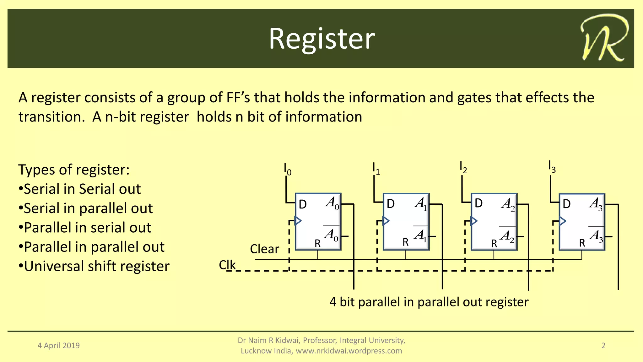
A register consists of a group of FF’s that holds the information and gates that effects the
transition. A n-bit register holds n bit of information
4 April 2019
Dr Naim R Kidwai, Professor, Integral University,
Lucknow India, www.nrkidwai.wordpress.com
2
Types of register:
•Serial in Serial out
•Serial in parallel out
•Parallel in serial out
•Parallel in parallel out
•Universal shift register
4 bit parallel in parallel out register
D 0A
0A
D 1A
1A
D 2A
2A
D 3A
3A
Clk
R R R R
I0 I1
I2 I3
Clear
Shift Register
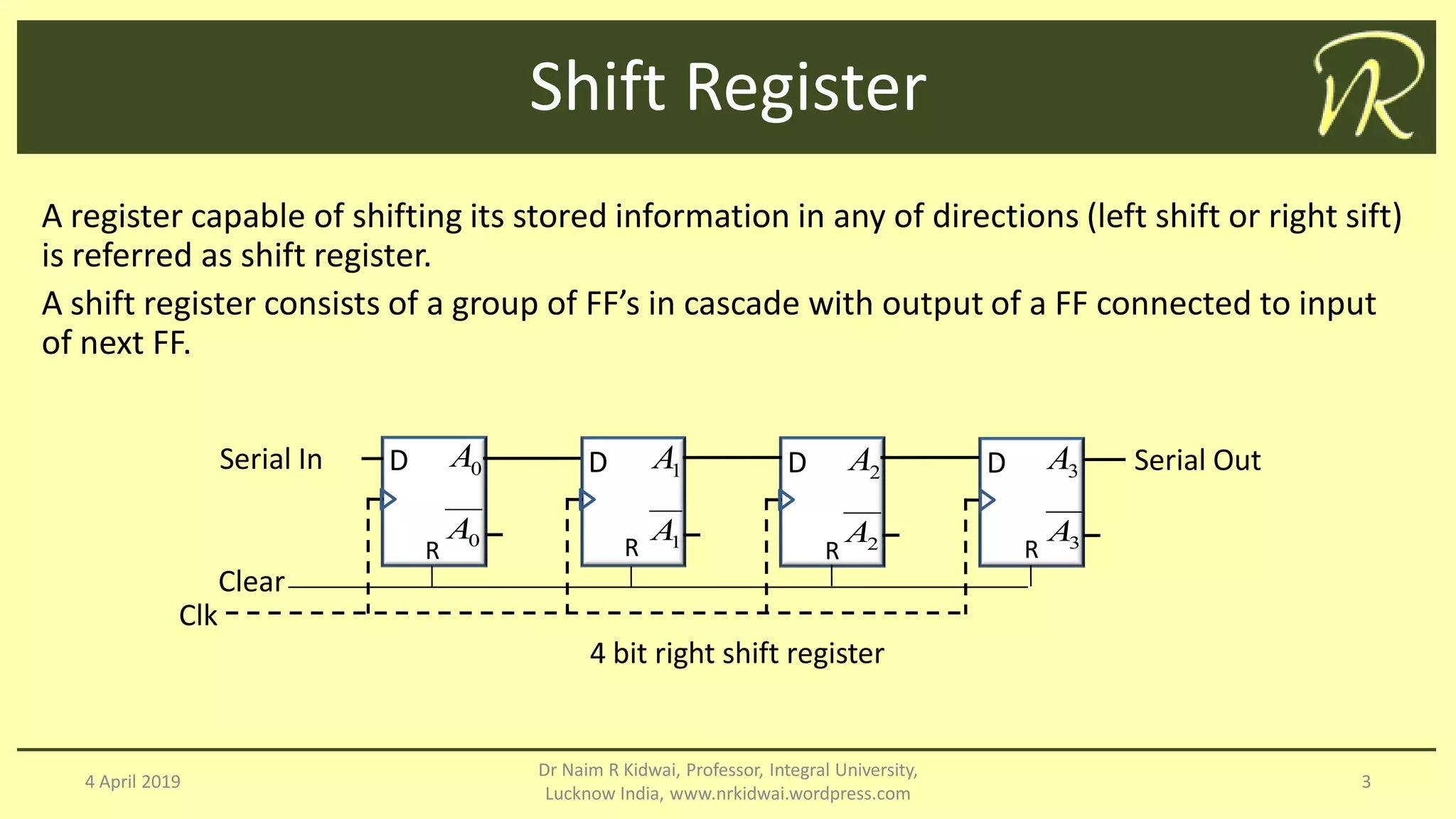
A register capable of shifting its stored information in any of directions (left shift or right sift)
is referred as shift register.
A shift register consists of a group of FF’s in cascade with output of a FF connected to input
of next FF.
4 April 2019
Dr Naim R Kidwai, Professor, Integral University,
Lucknow India, www.nrkidwai.wordpress.com
3
4 bit right shift register
D 0A
0A
D 1A
1A
D 2A
2A
D 3A
3A
Clk
R R R R
Serial In
Clear
Serial Out
Universal Shift Register
4 April 2019
Dr Naim R Kidwai, Professor, Integral University,
Lucknow India, www.nrkidwai.wordpress.com
4
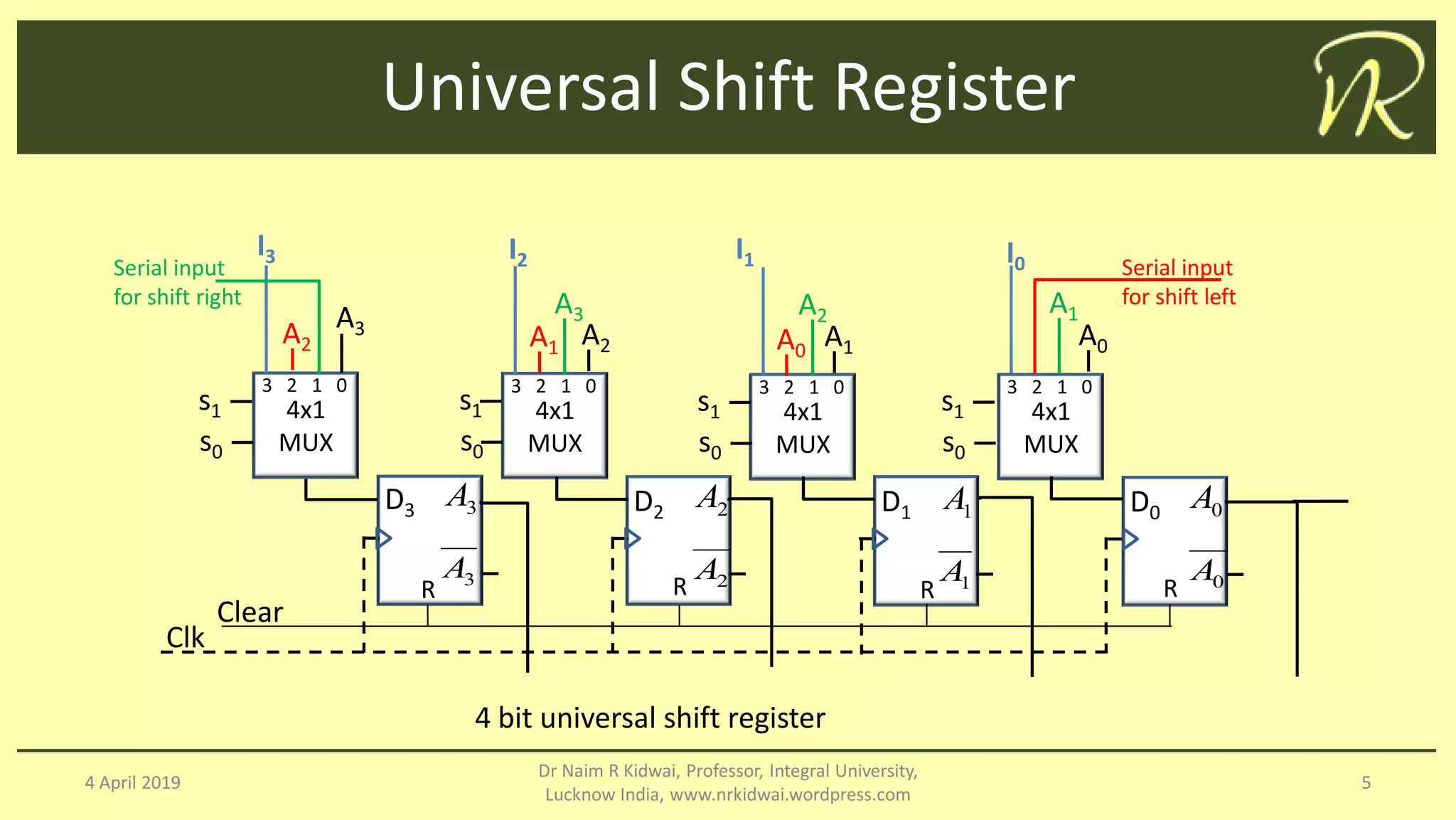
A universal shift register has following capabilities
• A clear input to reset all FF’s to ‘0’
• A clock input to synchronize all FF’s
• A shift right control to enable shift right operation and the serial input and output lines
associated with shift right
• A shift left control to enable shift right operation and the serial input and output lines
associated with shift left
• A parallel load with n input lines / n output lines
Universal Shift Register
4 April 2019
Dr Naim R Kidwai, Professor, Integral University,
Lucknow India, www.nrkidwai.wordpress.com
5
4 bit universal shift register
Clk
Clear
D3 3A
3A
R
D2 2A
2A
R
D1 1A
1A
R
D0 0A
0A
R
I2
4x1
MUX
3 2 1 0
I1
4x1
MUX
3 2 1 0
I0
4x1
MUX
3 2 1 0
I3
4x1
MUX
3 2 1 0
Serial input
for shift right
Serial input
for shift left
A3
A3 A2 A1
A0
A1
A2 A0A1A2
s1
s0
s1
s0
s1
s0
s1
s0
Counters
4 April 2019
Dr Naim R Kidwai, Professor, Integral University,
Lucknow India, www.nrkidwai.wordpress.com
6
Counter is a register that follows a pre-described sequence of states at application of input
pulses is called counter
Ripple counter: FF output transition serves as clock input to other FF’s
Synchronous counter: All FF’s of counter receive same clock pulse
Binary Counter: sequence of states follow binary sequence
Synchronous Counter design Example
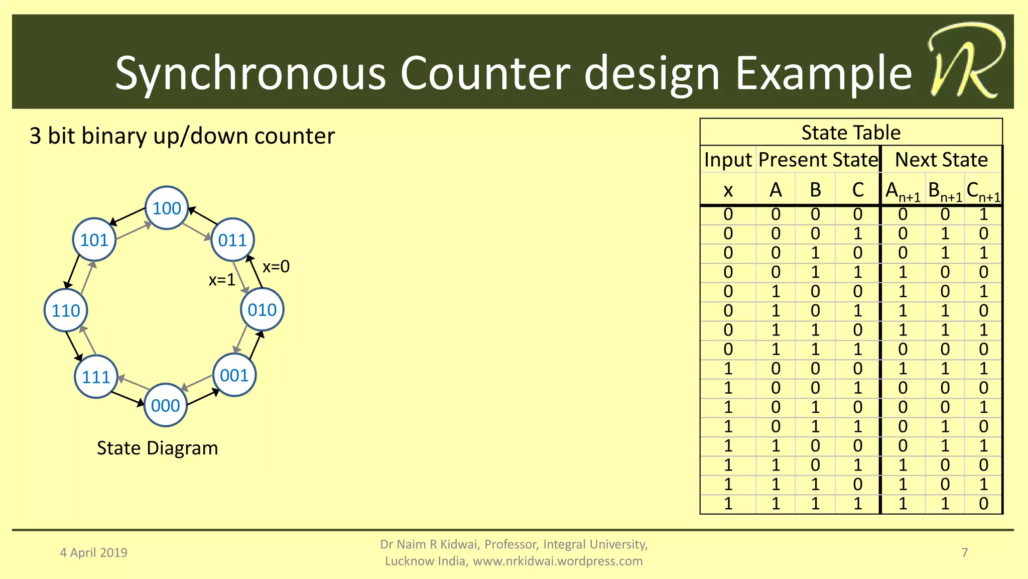
3 bit binary up/down counter
4 April 2019
Dr Naim R Kidwai, Professor, Integral University,
Lucknow India, www.nrkidwai.wordpress.com
7
State Table
Input Present State Next State
x A B C An+1 Bn+1 Cn+1
0 0 0 0 0 0 1
0 0 0 1 0 1 0
0 0 1 0 0 1 1
0 0 1 1 1 0 0
0 1 0 0 1 0 1
0 1 0 1 1 1 0
0 1 1 0 1 1 1
0 1 1 1 0 0 0
1 0 0 0 1 1 1
1 0 0 1 0 0 0
1 0 1 0 0 0 1
1 0 1 1 0 1 0
1 1 0 0 0 1 1
1 1 0 1 1 0 0
1 1 1 0 1 0 1
1 1 1 1 1 1 0
100
000
011
001
101
111
010110
x=1
x=0
State Diagram
Synchronous Counter design Example
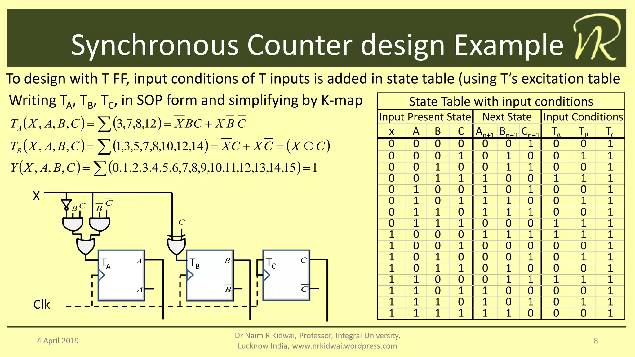
To design with T FF, input conditions of T inputs is added in state table (using T’s excitation table
4 April 2019
Dr Naim R Kidwai, Professor, Integral University,
Lucknow India, www.nrkidwai.wordpress.com
8
State Table with input conditions
Input Present State Next State Input Conditions
x A B C An+1 Bn+1 Cn+1 TA TB TC
0 0 0 0 0 0 1 0 0 1
0 0 0 1 0 1 0 0 1 1
0 0 1 0 0 1 1 0 0 1
0 0 1 1 1 0 0 1 1 1
0 1 0 0 1 0 1 0 0 1
0 1 0 1 1 1 0 0 1 1
0 1 1 0 1 1 1 0 0 1
0 1 1 1 0 0 0 1 1 1
1 0 0 0 1 1 1 1 1 1
1 0 0 1 0 0 0 0 0 1
1 0 1 0 0 0 1 0 1 1
1 0 1 1 0 1 0 0 0 1
1 1 0 0 0 1 1 1 1 1
1 1 0 1 1 0 0 0 0 1
1 1 1 0 1 0 1 0 1 1
1 1 1 1 1 1 0 0 0 1
   
     
    115,14,13,12,11,10,9,8,7,6.5.4.3.2.1.0,,,
14,12,10,8,7,5,3,1,,,
12,8,7,3,,,






CBAXY
CXCXCXCBAXT
CBXBCXCBAXT
B
A
X
TC
C
C
TB
B
B
TA
A
A
B C B
C
C
Clk
Writing TA, TB, TC, in SOP form and simplifying by K-map
Other Counters
4 April 2019
Dr Naim R Kidwai, Professor, Integral University,
Lucknow India, www.nrkidwai.wordpress.com
9
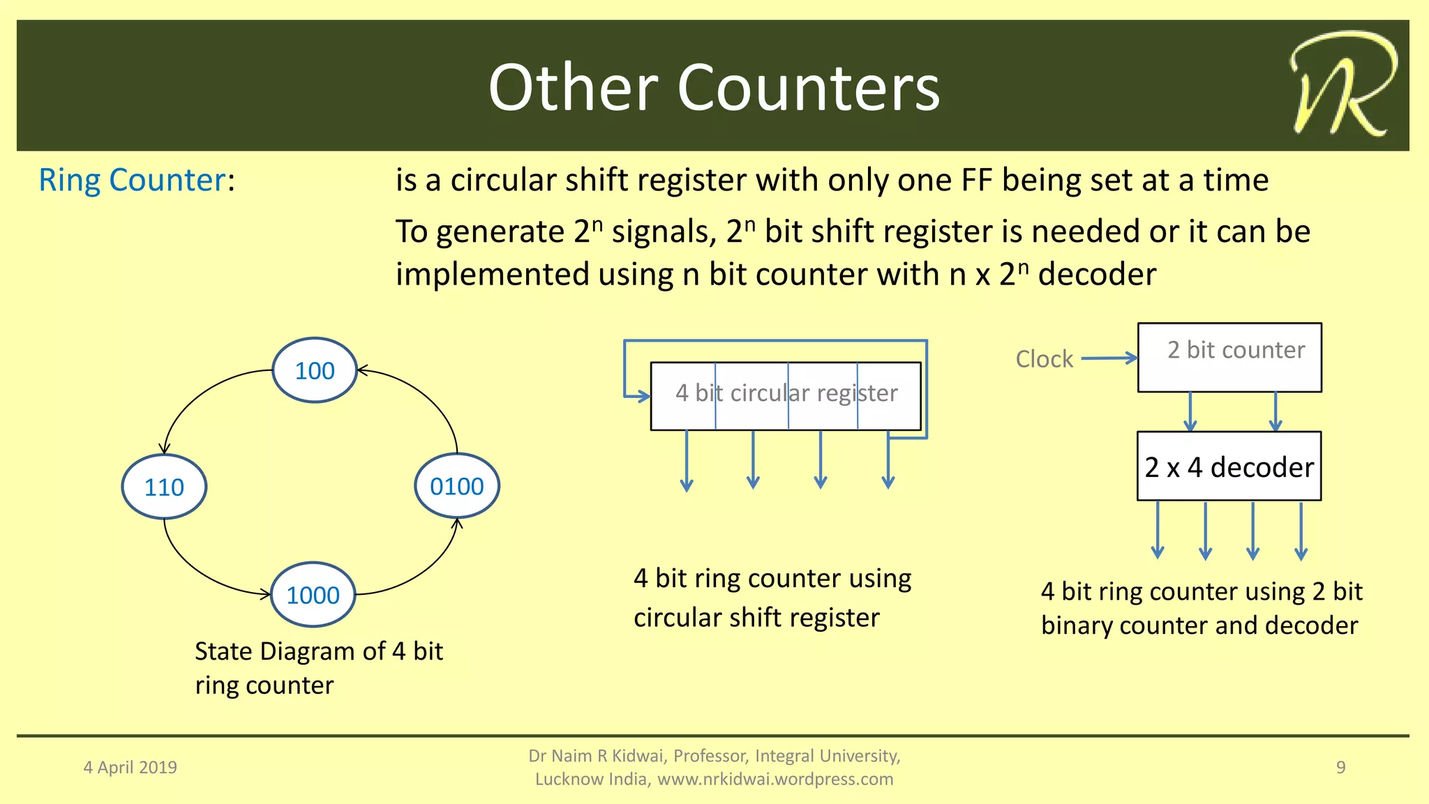
Ring Counter: is a circular shift register with only one FF being set at a time
To generate 2n signals, 2n bit shift register is needed or it can be
implemented using n bit counter with n x 2n decoder
4 bit circular register
2 bit counter
2 x 4 decoder
Clock100
1000
0100110
State Diagram of 4 bit
ring counter
4 bit ring counter using
circular shift register
4 bit ring counter using 2 bit
binary counter and decoder
Other Counters
4 April 2019
Dr Naim R Kidwai, Professor, Integral University,
Lucknow India, www.nrkidwai.wordpress.com
10
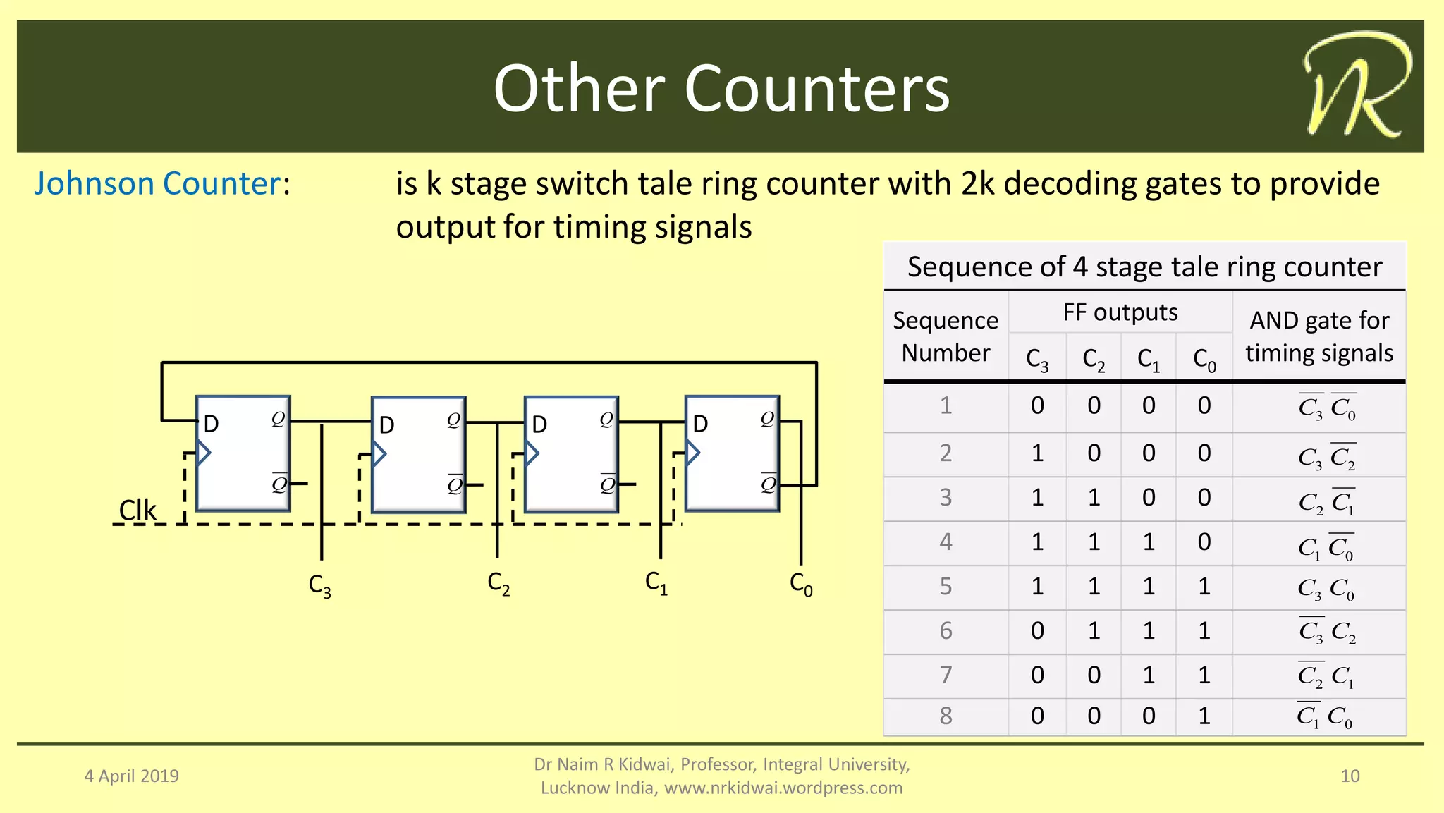
Johnson Counter: is k stage switch tale ring counter with 2k decoding gates to provide
output for timing signals
D Q
Q
Clk
D Q
Q
D Q
Q
D Q
Q
C3
C2 C1 C0
Sequence of 4 stage tale ring counter
Sequence
Number
FF outputs AND gate for
timing signalsC3 C2 C1 C0
1 0 0 0 0
2 1 0 0 0
3 1 1 0 0
4 1 1 1 0
5 1 1 1 1
6 0 1 1 1
7 0 0 1 1
8 0 0 0 1
03 CC
23 CC
12 CC
01 CC
03 CC
23 CC
12 CC
01 CC
Ripple Counter
4 April 2019
Dr Naim R Kidwai, Professor, Integral University,
Lucknow India, www.nrkidwai.wordpress.com
11
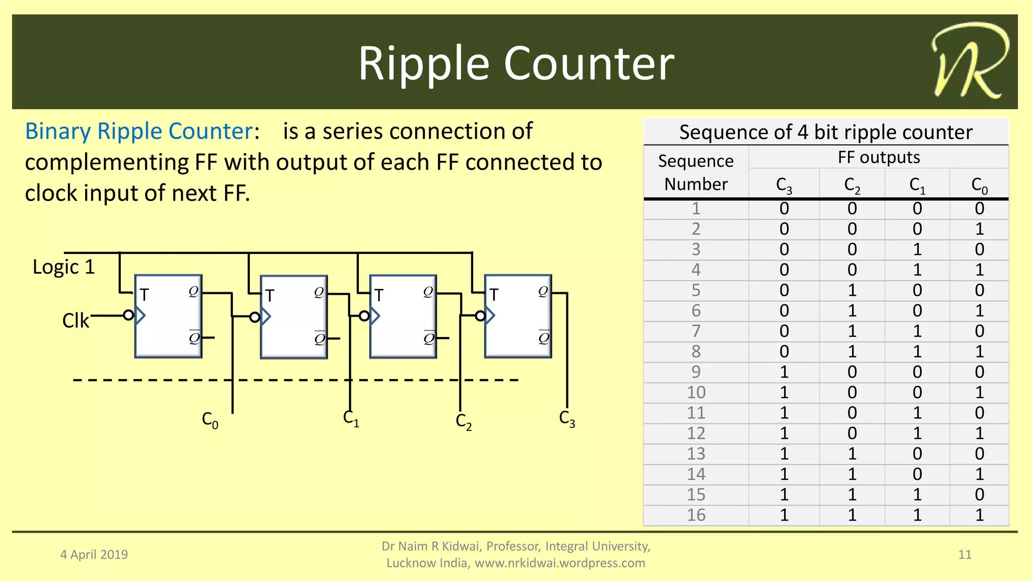
Binary Ripple Counter: is a series connection of
complementing FF with output of each FF connected to
clock input of next FF.
T Q
Q
Clk
T Q
Q
T Q
Q
T Q
Q
C0 C1 C2
C3
Sequence of 4 bit ripple counter
Sequence
Number
FF outputs
C3 C2 C1 C0
1 0 0 0 0
2 0 0 0 1
3 0 0 1 0
4 0 0 1 1
5 0 1 0 0
6 0 1 0 1
7 0 1 1 0
8 0 1 1 1
9 1 0 0 0
10 1 0 0 1
11 1 0 1 0
12 1 0 1 1
13 1 1 0 0
14 1 1 0 1
15 1 1 1 0
16 1 1 1 1
Logic 1
BCD Ripple Counter
4 April 2019
Dr Naim R Kidwai, Professor, Integral University,
Lucknow India, www.nrkidwai.wordpress.com
12
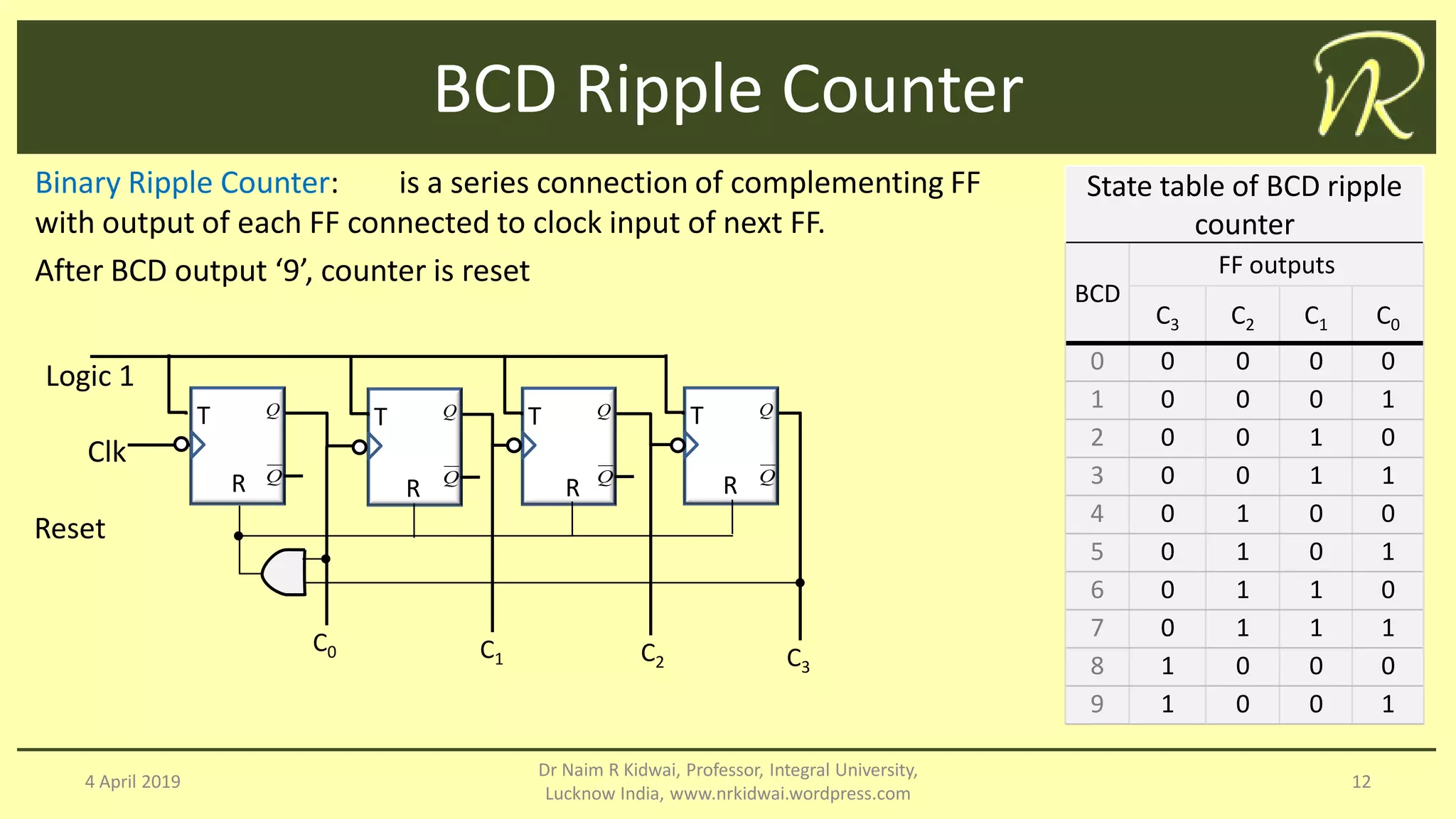
Binary Ripple Counter: is a series connection of complementing FF
with output of each FF connected to clock input of next FF.
After BCD output ‘9’, counter is reset
State table of BCD ripple
counter
BCD
FF outputs
C3 C2 C1 C0
0 0 0 0 0
1 0 0 0 1
2 0 0 1 0
3 0 0 1 1
4 0 1 0 0
5 0 1 0 1
6 0 1 1 0
7 0 1 1 1
8 1 0 0 0
9 1 0 0 1
T Q
Q
Clk
T Q
Q
T Q
Q
T Q
Q
C0 C1 C2 C3
Logic 1
Reset
R R R R

synchronous Sequential circuit counters and registers

  • 1.
    Clocked Sequential Circuit:Registers and Counters 4 April 2019 1 Dr Naim R Kidwai, Professor, Integral University, Lucknow India, www.nrkidwai.wordpress.com Learning Objectives: 1. To learn about registers/ shift registers 2. To learn about design and analysis of counters 3. To learn design of ripple counters
  • 2.
    Register A register consistsof a group of FF’s that holds the information and gates that effects the transition. A n-bit register holds n bit of information 4 April 2019 Dr Naim R Kidwai, Professor, Integral University, Lucknow India, www.nrkidwai.wordpress.com 2 Types of register: •Serial in Serial out •Serial in parallel out •Parallel in serial out •Parallel in parallel out •Universal shift register 4 bit parallel in parallel out register D 0A 0A D 1A 1A D 2A 2A D 3A 3A Clk R R R R I0 I1 I2 I3 Clear
  • 3.
    Shift Register A registercapable of shifting its stored information in any of directions (left shift or right sift) is referred as shift register. A shift register consists of a group of FF’s in cascade with output of a FF connected to input of next FF. 4 April 2019 Dr Naim R Kidwai, Professor, Integral University, Lucknow India, www.nrkidwai.wordpress.com 3 4 bit right shift register D 0A 0A D 1A 1A D 2A 2A D 3A 3A Clk R R R R Serial In Clear Serial Out
  • 4.
    Universal Shift Register 4April 2019 Dr Naim R Kidwai, Professor, Integral University, Lucknow India, www.nrkidwai.wordpress.com 4 A universal shift register has following capabilities • A clear input to reset all FF’s to ‘0’ • A clock input to synchronize all FF’s • A shift right control to enable shift right operation and the serial input and output lines associated with shift right • A shift left control to enable shift right operation and the serial input and output lines associated with shift left • A parallel load with n input lines / n output lines
  • 5.
    Universal Shift Register 4April 2019 Dr Naim R Kidwai, Professor, Integral University, Lucknow India, www.nrkidwai.wordpress.com 5 4 bit universal shift register Clk Clear D3 3A 3A R D2 2A 2A R D1 1A 1A R D0 0A 0A R I2 4x1 MUX 3 2 1 0 I1 4x1 MUX 3 2 1 0 I0 4x1 MUX 3 2 1 0 I3 4x1 MUX 3 2 1 0 Serial input for shift right Serial input for shift left A3 A3 A2 A1 A0 A1 A2 A0A1A2 s1 s0 s1 s0 s1 s0 s1 s0
  • 6.
    Counters 4 April 2019 DrNaim R Kidwai, Professor, Integral University, Lucknow India, www.nrkidwai.wordpress.com 6 Counter is a register that follows a pre-described sequence of states at application of input pulses is called counter Ripple counter: FF output transition serves as clock input to other FF’s Synchronous counter: All FF’s of counter receive same clock pulse Binary Counter: sequence of states follow binary sequence
  • 7.
    Synchronous Counter designExample 3 bit binary up/down counter 4 April 2019 Dr Naim R Kidwai, Professor, Integral University, Lucknow India, www.nrkidwai.wordpress.com 7 State Table Input Present State Next State x A B C An+1 Bn+1 Cn+1 0 0 0 0 0 0 1 0 0 0 1 0 1 0 0 0 1 0 0 1 1 0 0 1 1 1 0 0 0 1 0 0 1 0 1 0 1 0 1 1 1 0 0 1 1 0 1 1 1 0 1 1 1 0 0 0 1 0 0 0 1 1 1 1 0 0 1 0 0 0 1 0 1 0 0 0 1 1 0 1 1 0 1 0 1 1 0 0 0 1 1 1 1 0 1 1 0 0 1 1 1 0 1 0 1 1 1 1 1 1 1 0 100 000 011 001 101 111 010110 x=1 x=0 State Diagram
  • 8.
    Synchronous Counter designExample To design with T FF, input conditions of T inputs is added in state table (using T’s excitation table 4 April 2019 Dr Naim R Kidwai, Professor, Integral University, Lucknow India, www.nrkidwai.wordpress.com 8 State Table with input conditions Input Present State Next State Input Conditions x A B C An+1 Bn+1 Cn+1 TA TB TC 0 0 0 0 0 0 1 0 0 1 0 0 0 1 0 1 0 0 1 1 0 0 1 0 0 1 1 0 0 1 0 0 1 1 1 0 0 1 1 1 0 1 0 0 1 0 1 0 0 1 0 1 0 1 1 1 0 0 1 1 0 1 1 0 1 1 1 0 0 1 0 1 1 1 0 0 0 1 1 1 1 0 0 0 1 1 1 1 1 1 1 0 0 1 0 0 0 0 0 1 1 0 1 0 0 0 1 0 1 1 1 0 1 1 0 1 0 0 0 1 1 1 0 0 0 1 1 1 1 1 1 1 0 1 1 0 0 0 0 1 1 1 1 0 1 0 1 0 1 1 1 1 1 1 1 1 0 0 0 1               115,14,13,12,11,10,9,8,7,6.5.4.3.2.1.0,,, 14,12,10,8,7,5,3,1,,, 12,8,7,3,,,       CBAXY CXCXCXCBAXT CBXBCXCBAXT B A X TC C C TB B B TA A A B C B C C Clk Writing TA, TB, TC, in SOP form and simplifying by K-map
  • 9.
    Other Counters 4 April2019 Dr Naim R Kidwai, Professor, Integral University, Lucknow India, www.nrkidwai.wordpress.com 9 Ring Counter: is a circular shift register with only one FF being set at a time To generate 2n signals, 2n bit shift register is needed or it can be implemented using n bit counter with n x 2n decoder 4 bit circular register 2 bit counter 2 x 4 decoder Clock100 1000 0100110 State Diagram of 4 bit ring counter 4 bit ring counter using circular shift register 4 bit ring counter using 2 bit binary counter and decoder
  • 10.
    Other Counters 4 April2019 Dr Naim R Kidwai, Professor, Integral University, Lucknow India, www.nrkidwai.wordpress.com 10 Johnson Counter: is k stage switch tale ring counter with 2k decoding gates to provide output for timing signals D Q Q Clk D Q Q D Q Q D Q Q C3 C2 C1 C0 Sequence of 4 stage tale ring counter Sequence Number FF outputs AND gate for timing signalsC3 C2 C1 C0 1 0 0 0 0 2 1 0 0 0 3 1 1 0 0 4 1 1 1 0 5 1 1 1 1 6 0 1 1 1 7 0 0 1 1 8 0 0 0 1 03 CC 23 CC 12 CC 01 CC 03 CC 23 CC 12 CC 01 CC
  • 11.
    Ripple Counter 4 April2019 Dr Naim R Kidwai, Professor, Integral University, Lucknow India, www.nrkidwai.wordpress.com 11 Binary Ripple Counter: is a series connection of complementing FF with output of each FF connected to clock input of next FF. T Q Q Clk T Q Q T Q Q T Q Q C0 C1 C2 C3 Sequence of 4 bit ripple counter Sequence Number FF outputs C3 C2 C1 C0 1 0 0 0 0 2 0 0 0 1 3 0 0 1 0 4 0 0 1 1 5 0 1 0 0 6 0 1 0 1 7 0 1 1 0 8 0 1 1 1 9 1 0 0 0 10 1 0 0 1 11 1 0 1 0 12 1 0 1 1 13 1 1 0 0 14 1 1 0 1 15 1 1 1 0 16 1 1 1 1 Logic 1
  • 12.
    BCD Ripple Counter 4April 2019 Dr Naim R Kidwai, Professor, Integral University, Lucknow India, www.nrkidwai.wordpress.com 12 Binary Ripple Counter: is a series connection of complementing FF with output of each FF connected to clock input of next FF. After BCD output ‘9’, counter is reset State table of BCD ripple counter BCD FF outputs C3 C2 C1 C0 0 0 0 0 0 1 0 0 0 1 2 0 0 1 0 3 0 0 1 1 4 0 1 0 0 5 0 1 0 1 6 0 1 1 0 7 0 1 1 1 8 1 0 0 0 9 1 0 0 1 T Q Q Clk T Q Q T Q Q T Q Q C0 C1 C2 C3 Logic 1 Reset R R R R