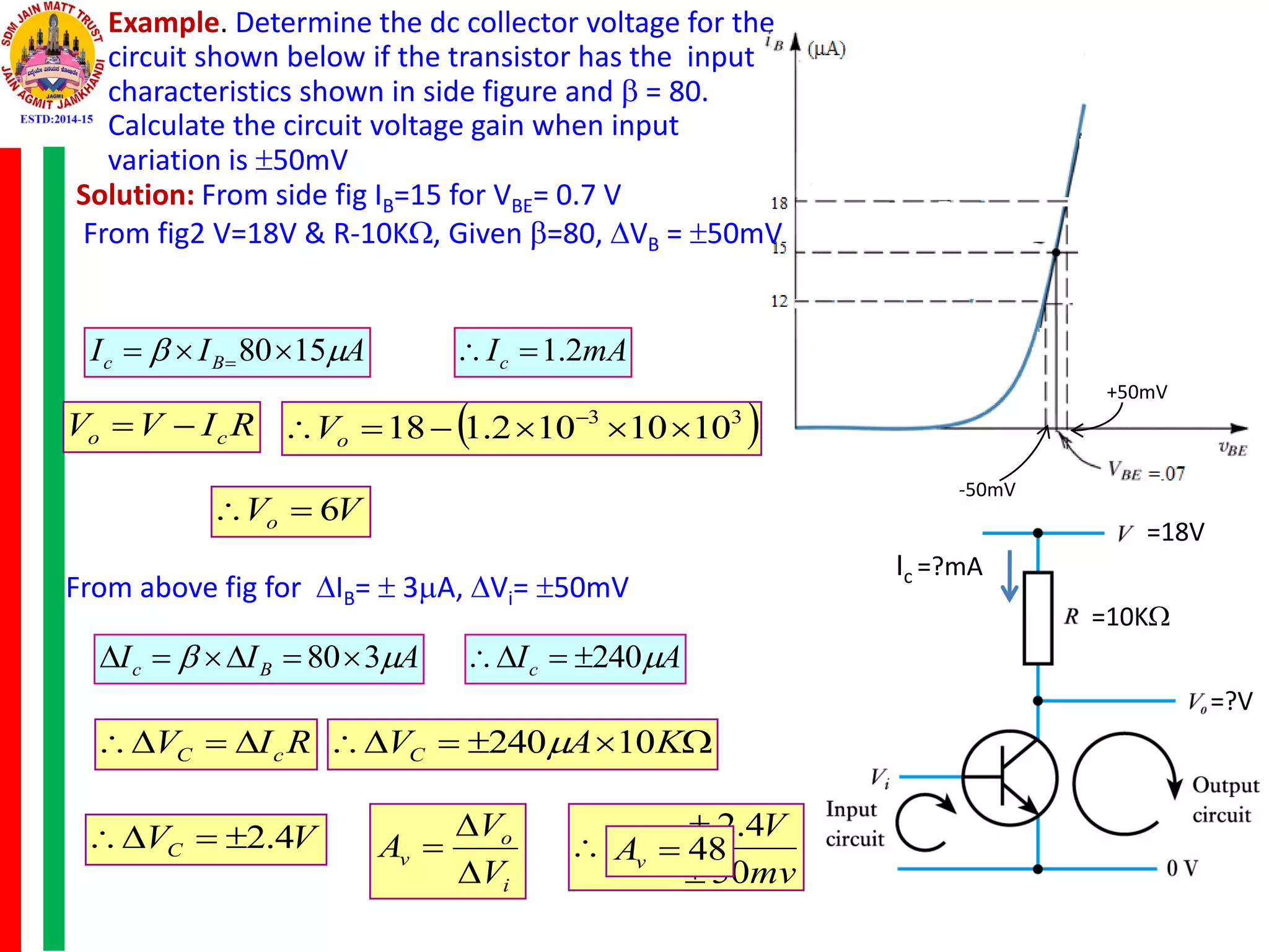
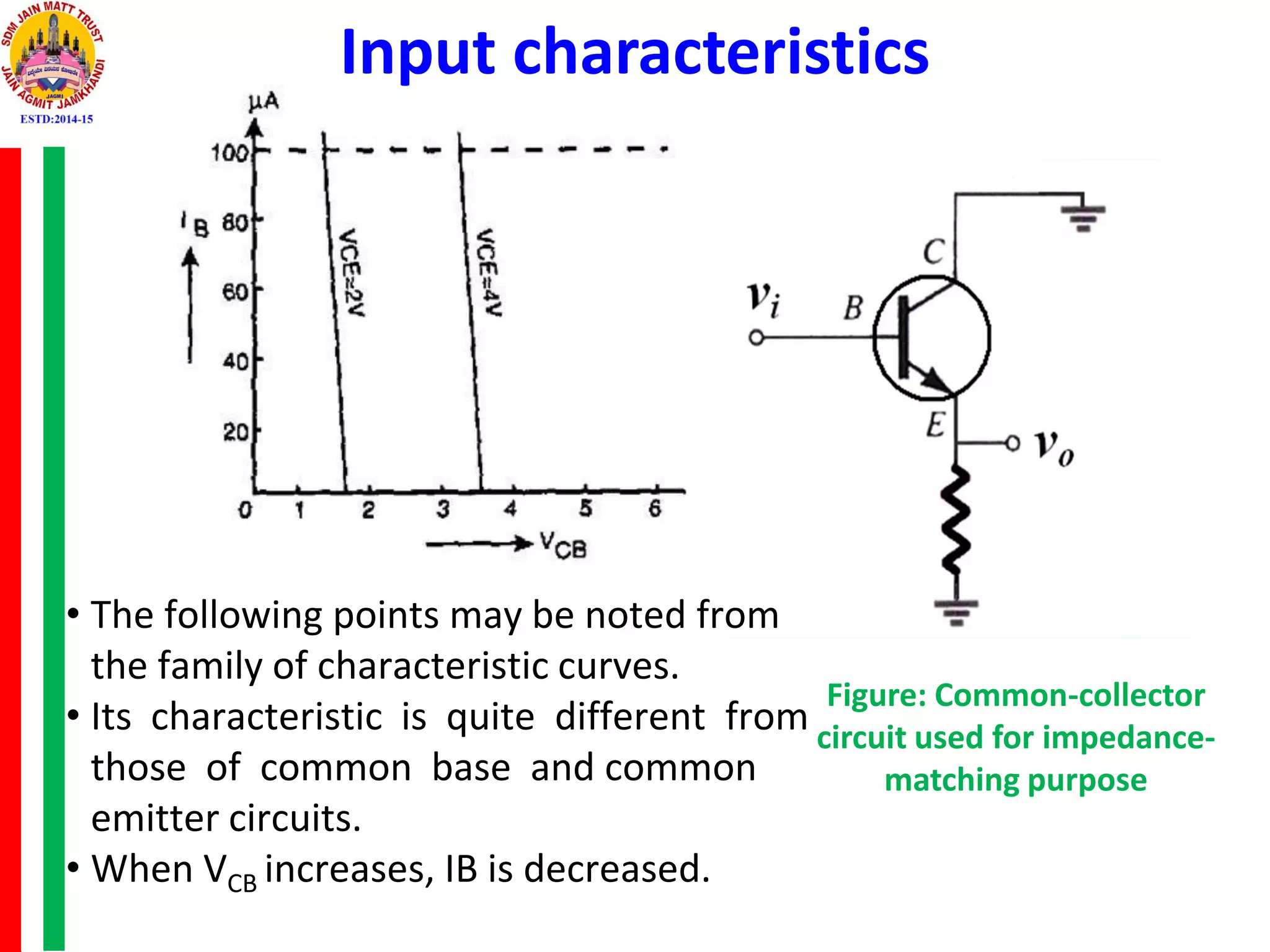
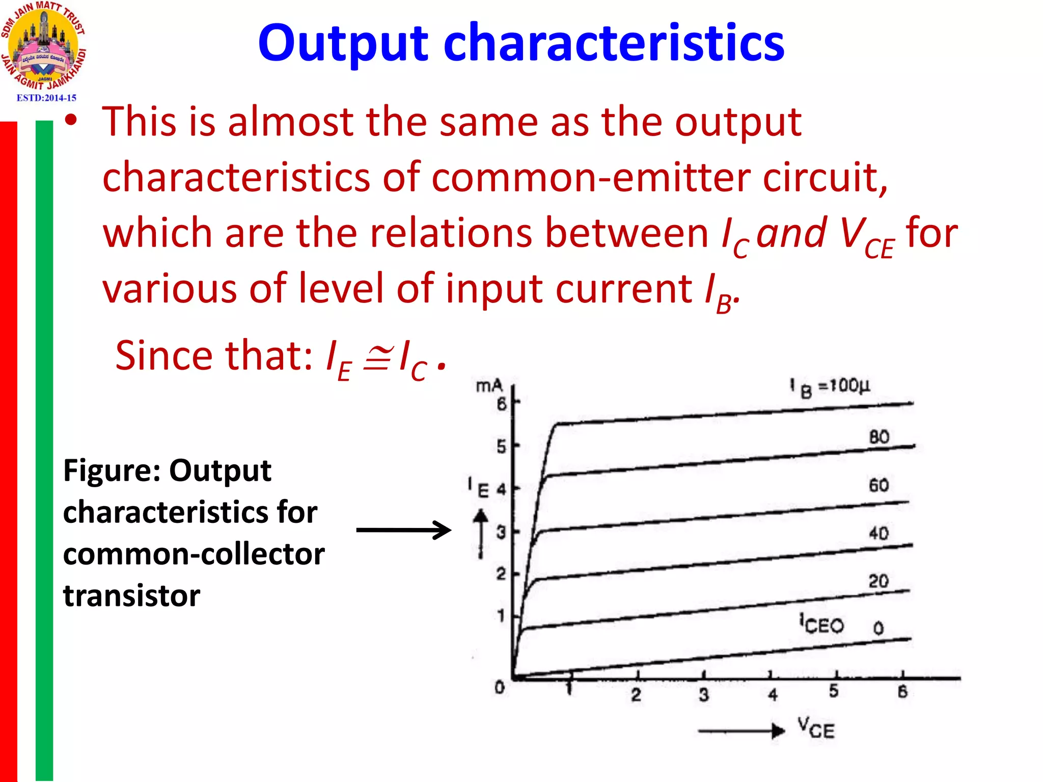
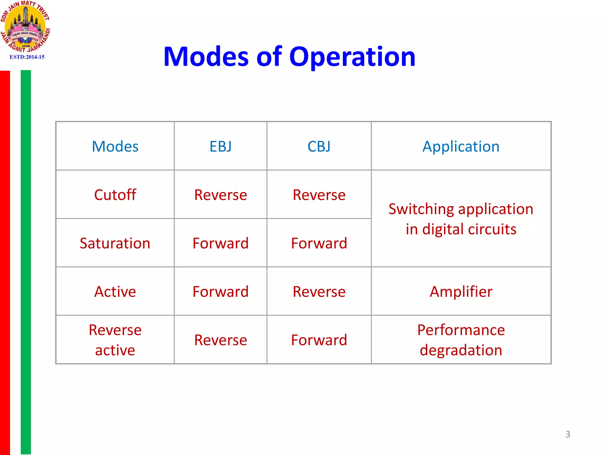
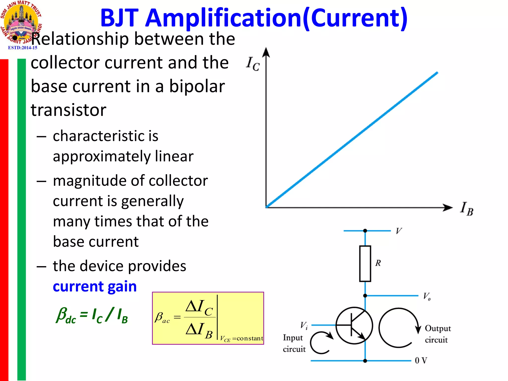
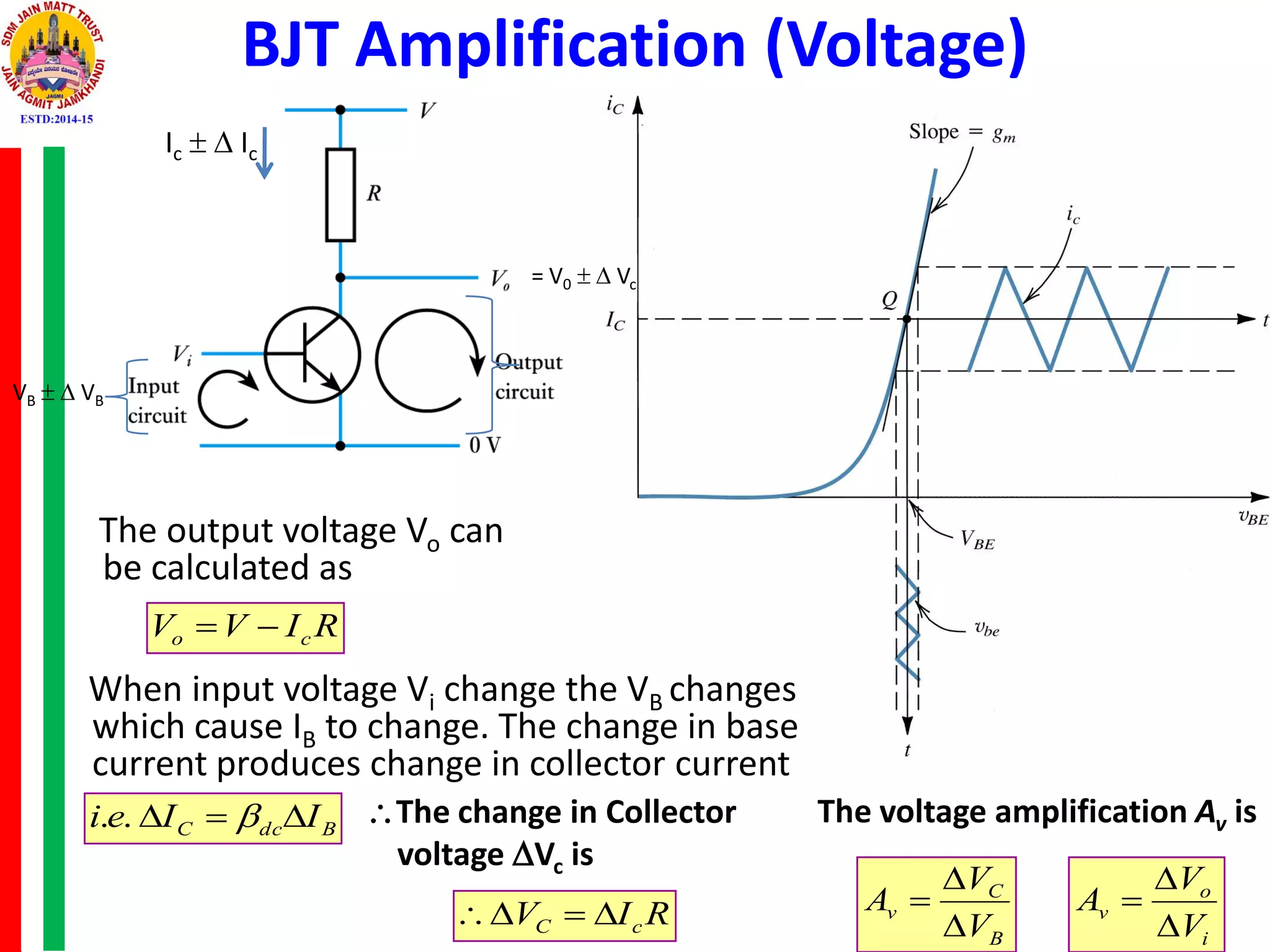
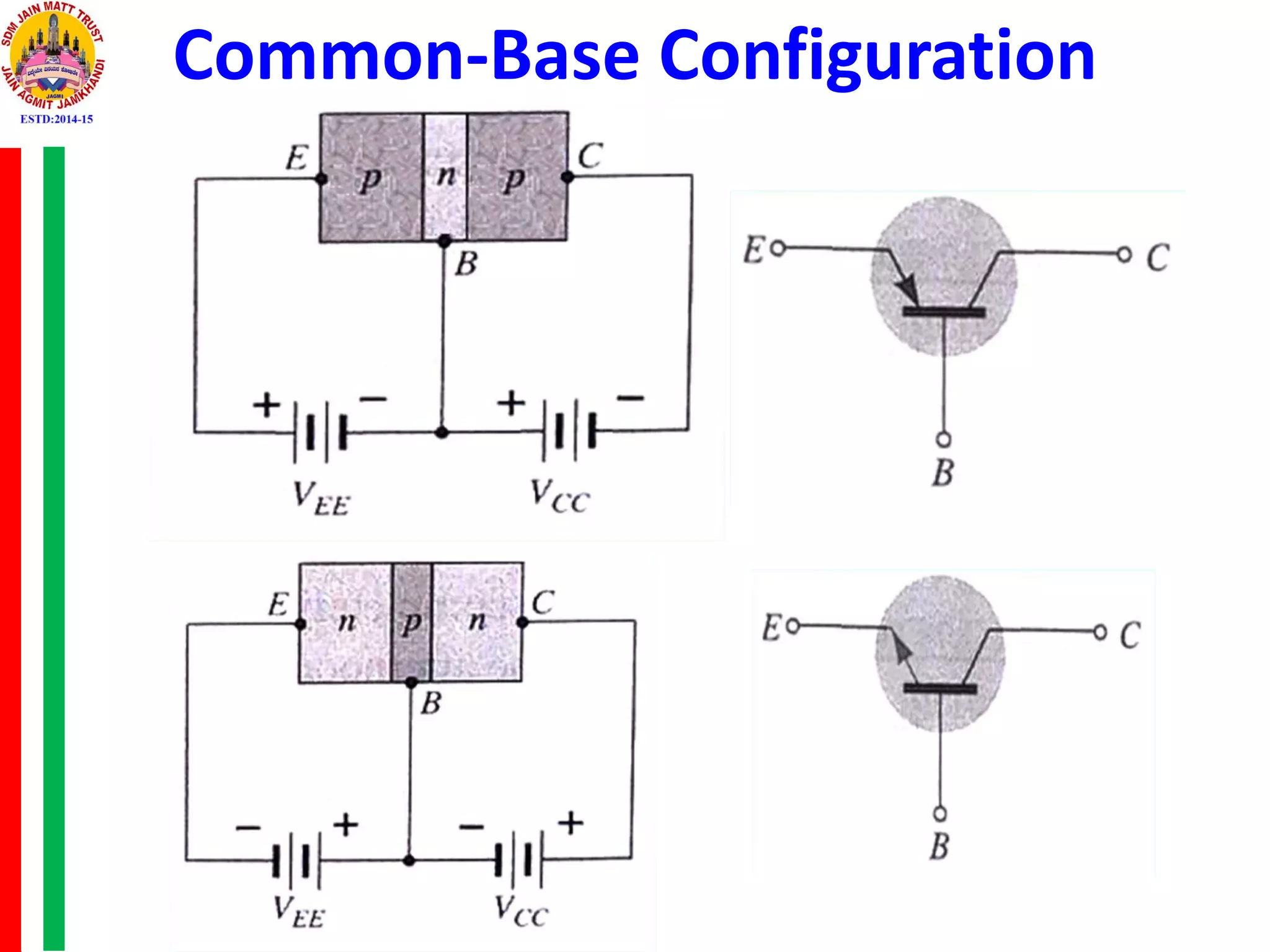
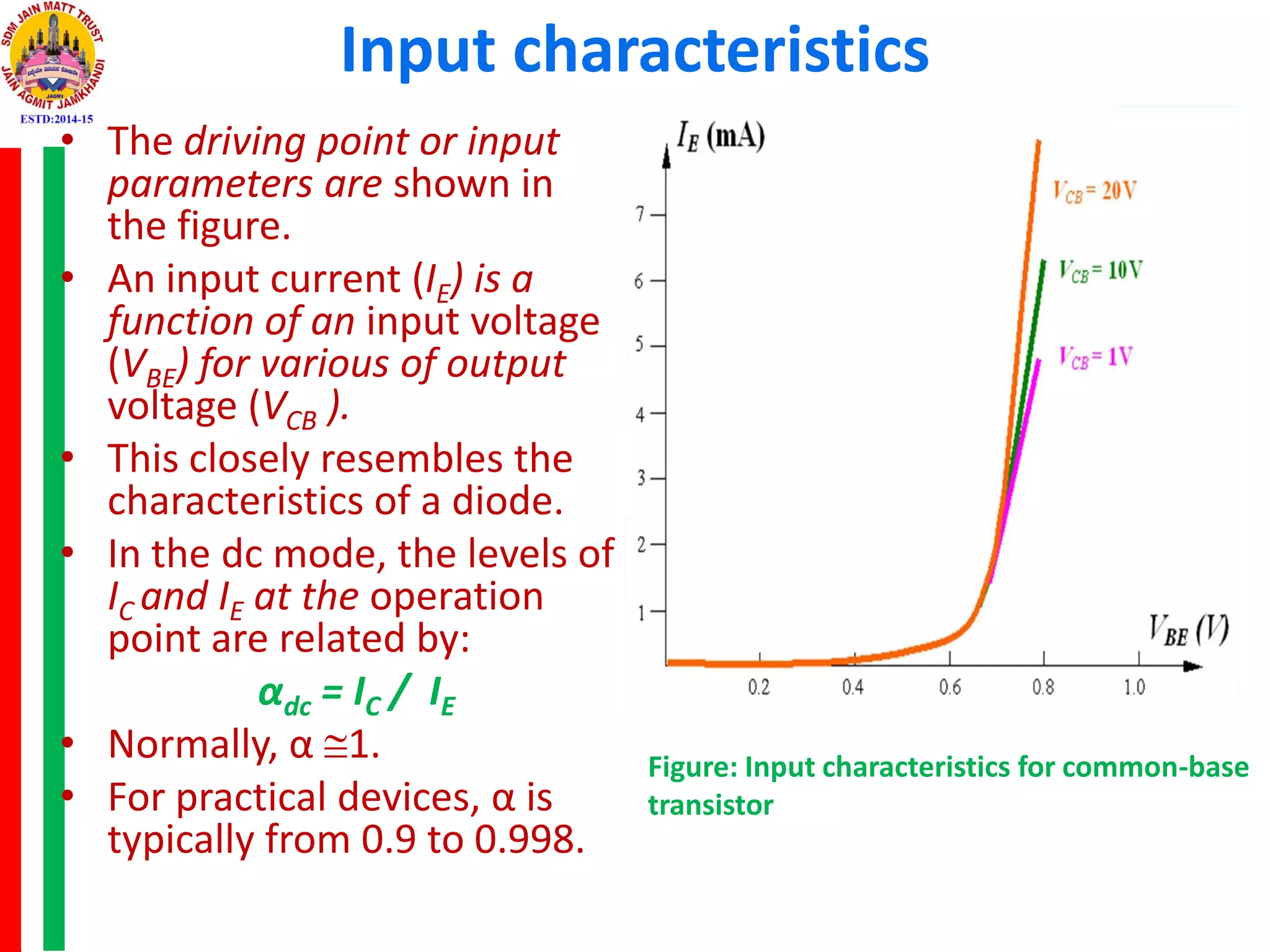
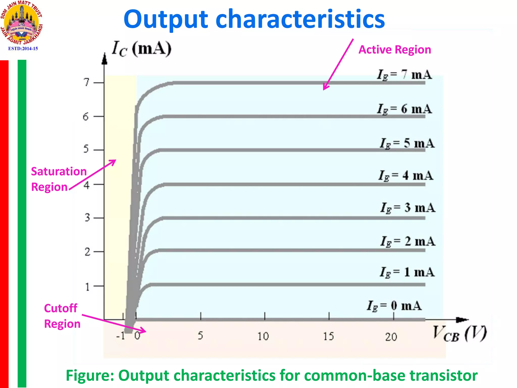
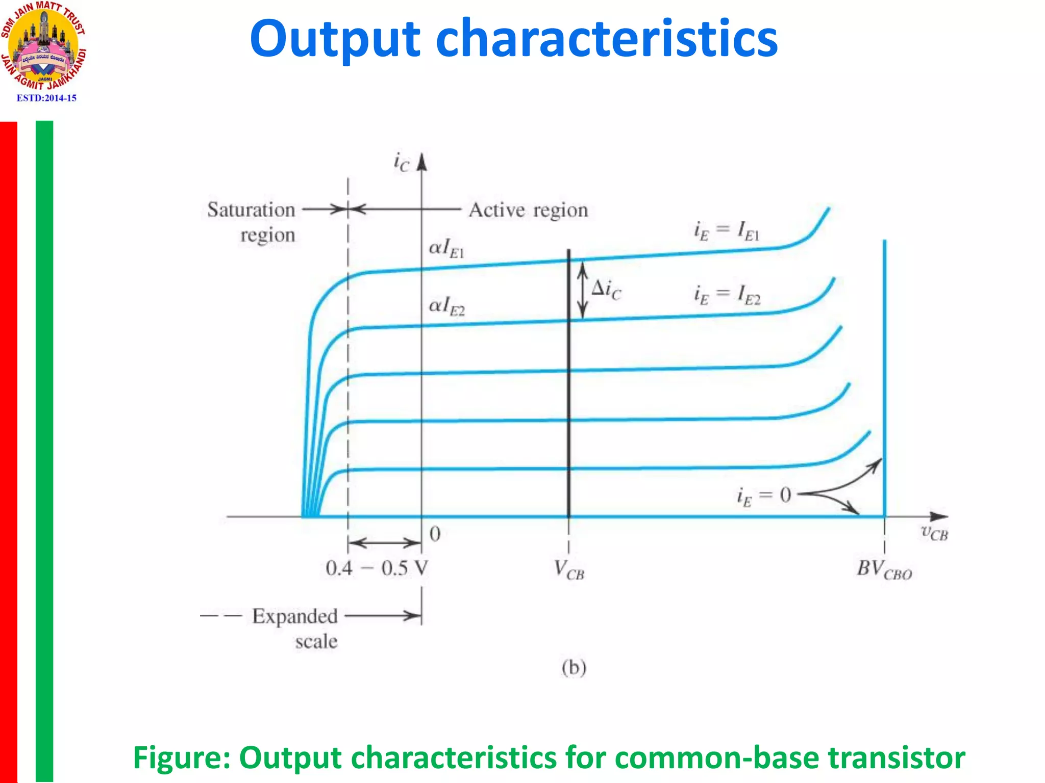
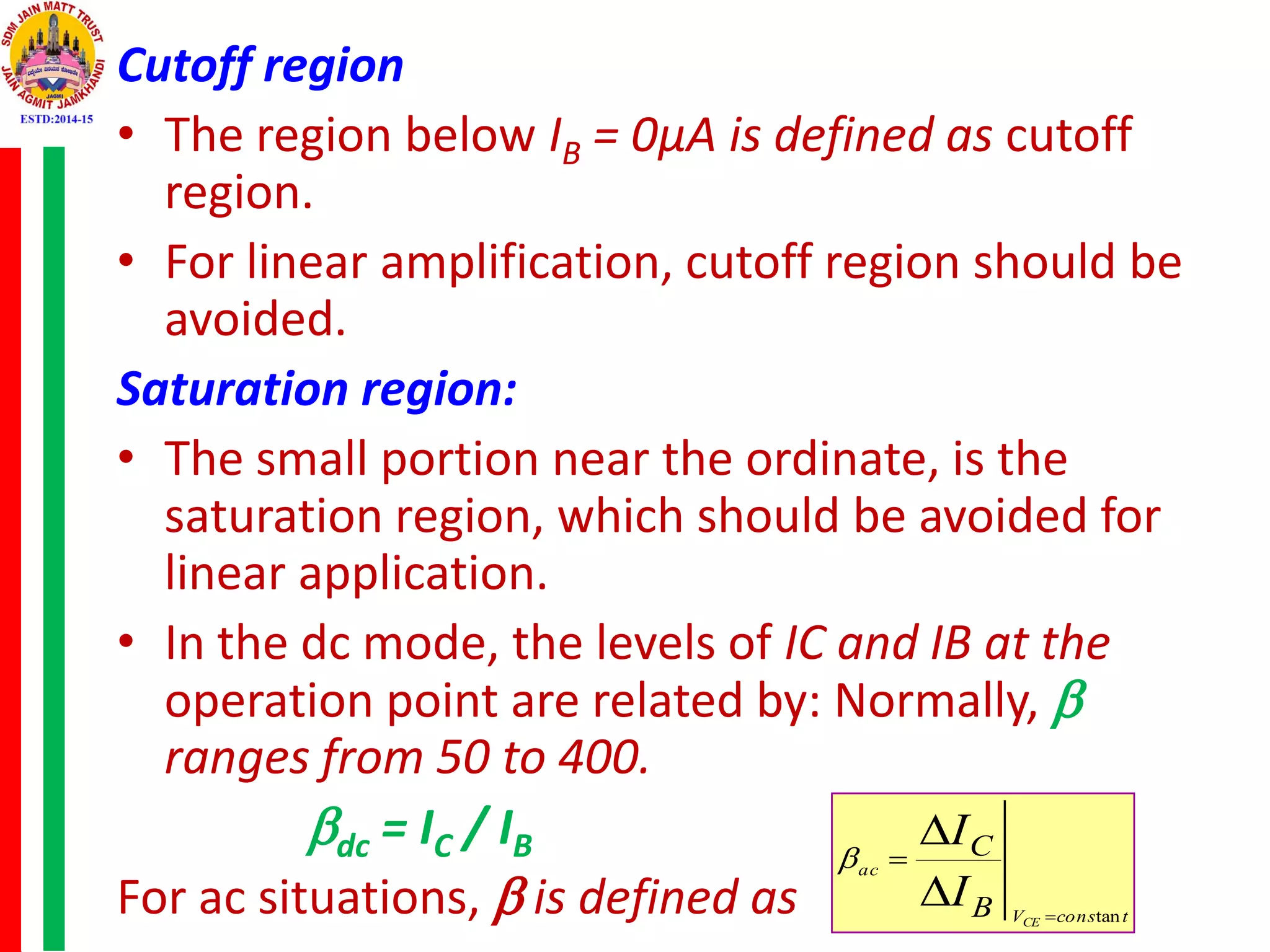
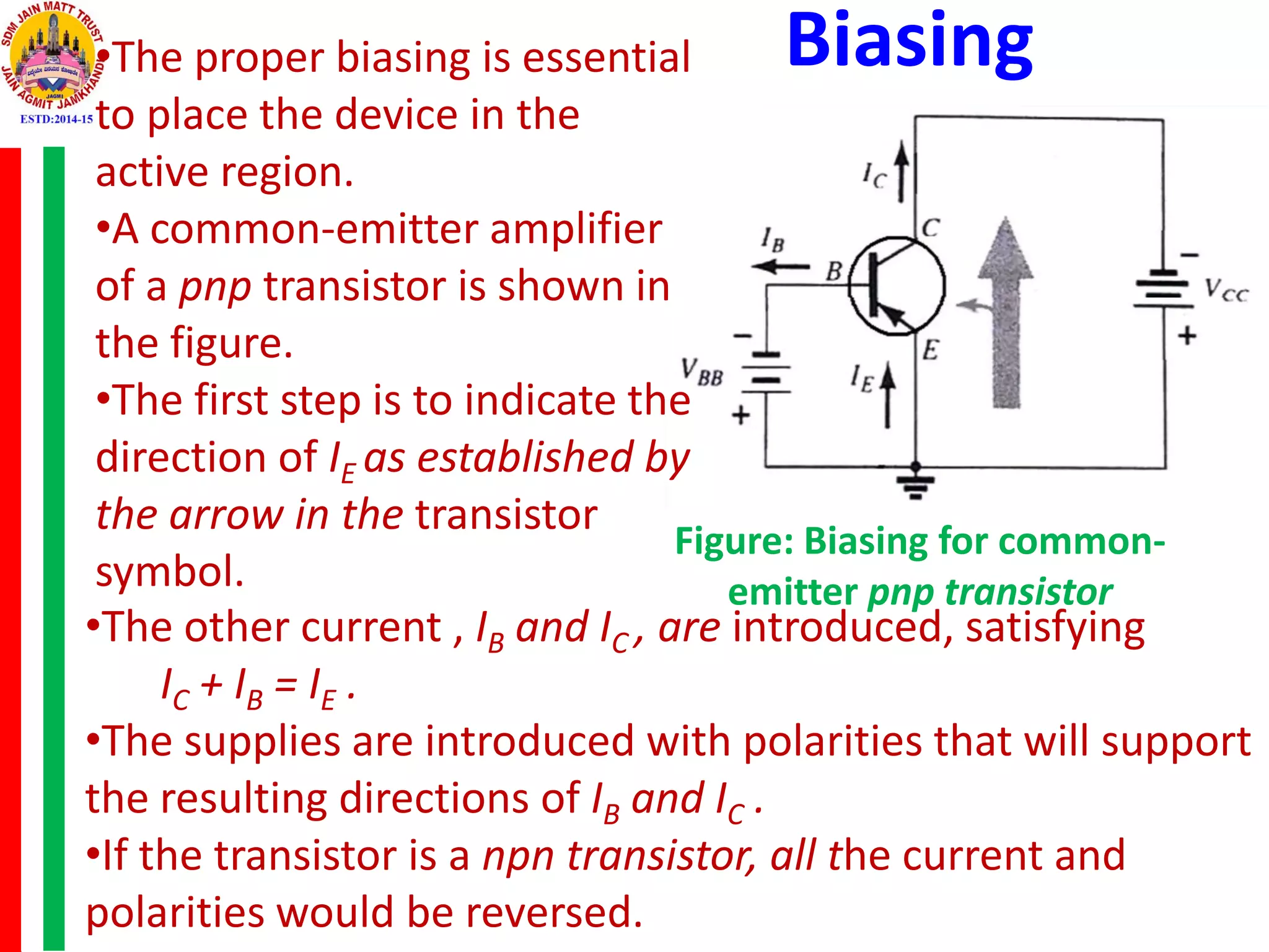
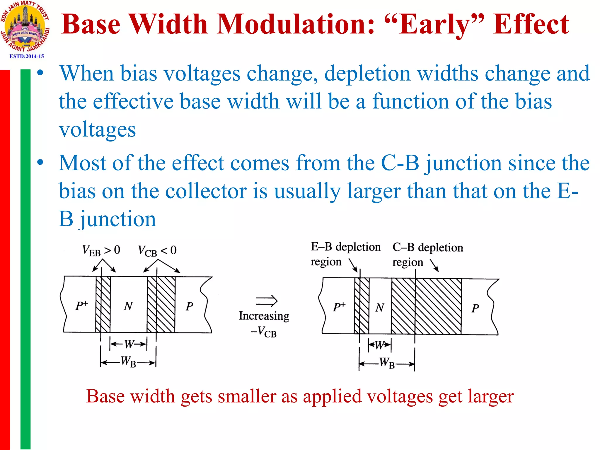
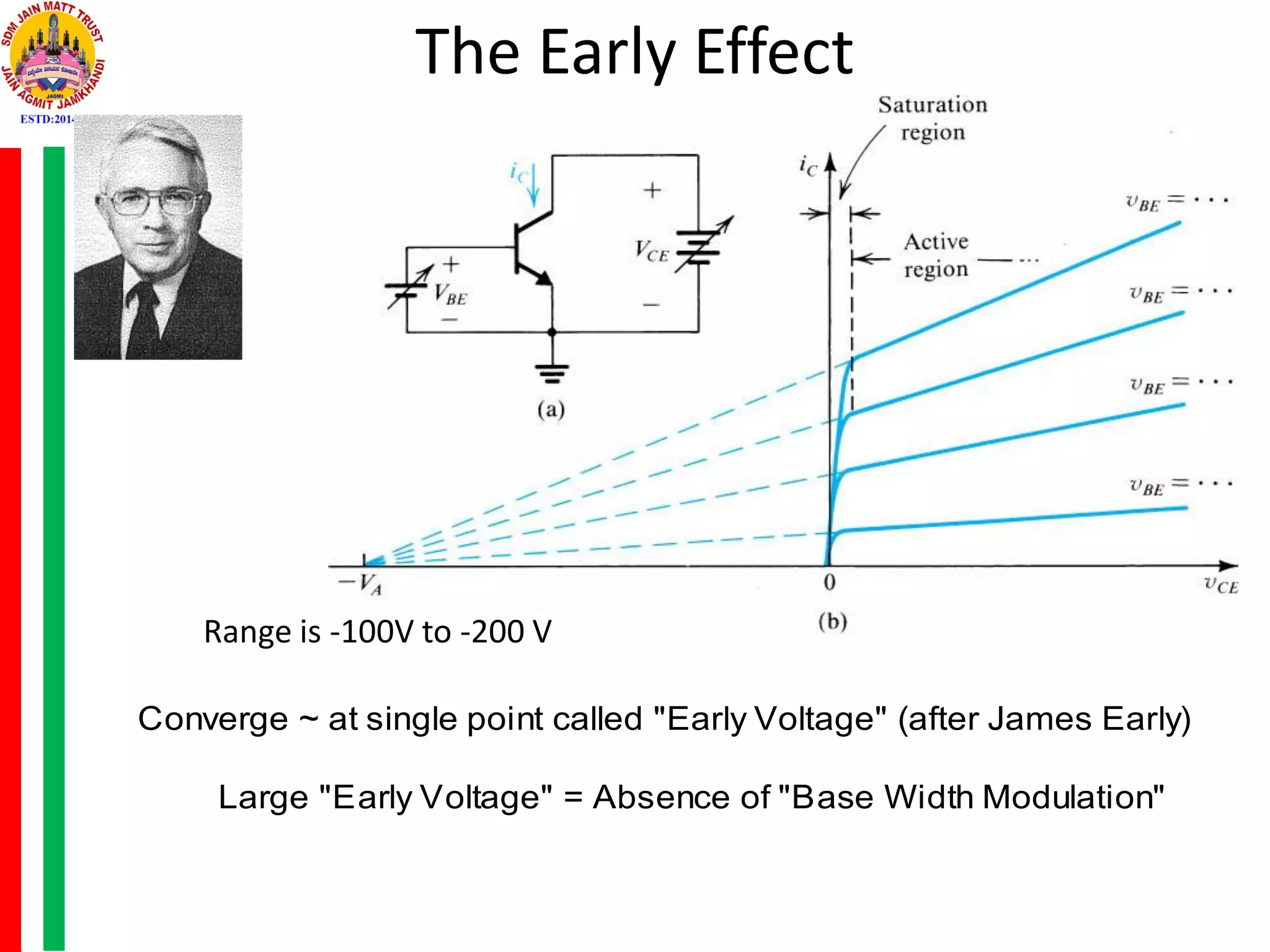
This document discusses various transistor configurations and their characteristics. It begins with a quote by Albert Einstein. It then discusses the common-base, common-emitter, and common-collector configurations. For each configuration, it describes the input and output characteristics, showing how the input and output currents and voltages relate. It notes that the common-emitter configuration is most commonly used and describes how to properly bias a common-emitter amplifier. The document also briefly discusses the early effect in transistors.
I presented this slid in my last presentation about bipolar junction transistor configuration.Now I'm sharing this with all of you guys it can be helpful for you.
Look at the beautiful view of forgiveness of mistakes.
Thank you
The three terminals of the FET are known as Gate, Drain, and Source.
It is a voltage controlled device, where the input voltage controls by the output current.
In FET current used to flow between the drain and the source terminal. And this current can be controlled by applying the voltage between the gate and the source terminal.
So this applied voltage generate the electric field within the device and by controlling these electric field we can control the flow of current through the device.
In this configuration base is common for both input and output, input signal is applied between emitter and base terminals; and output is collected between collector and base terminals. Copy the link given below and paste it in new browser window to get more information on Common Emitter Configuration:- http://www.transtutors.com/homework-help/electrical-engineering/transistors/common-emitter-configuration.aspx
The study of the basics of electronics can be studied through the link http://bit.ly/2PPv0mv
The transistor is a semiconductor device with three connections, capable of amplification in addition to rectification
Introduction to operational Amplifier. For A2 level physics (CIE). Discusses characteristics of op amp, inverting and non inverting amplifier, and voltage follower, and transfer characetristics, virtual earth , etc
Original Uni-junction transistor or UJT is a simple device in which a bar of N-type semiconductor material into which P-type material is diffused; somewhere along its length defining the device parameter as intrinsic standoff. The 2N2646 is the most commonly used version of UJT.
UNIT - II
BJTs: Transistor characteristics: The junction transistor, transistor as an amplifier, CB, CE, CC configurations, comparison of transistor configurations, the operating point, self-bias or Emitter bias, bias compensation, thermal runaway and stability, transistor at low frequencies, CE amplifier response, gain bandwidth product, Emitter follower, RC coupled amplifier, two cascaded CE and multi stage CE amplifiers.
1. Transistor Configuration
Quote of the day
“Try not to become a man of success,
but rather try to become a man of
value.”
― Albert Einstein
2.
3. Modes of Operation
3
Modes EBJ CBJ Application
Cutoff Reverse Reverse
Switching application
in digital circuits
Saturation Forward Forward
Active Forward Reverse Amplifier
Reverse
active
Reverse Forward
Performance
degradation
4. • Relationship between the
collector current and the
base current in a bipolar
transistor
– characteristic is
approximately linear
– magnitude of collector
current is generally
many times that of the
base current
– the device provides
current gain
B
C
I
I
CEV
ac
constant
dc = IC / IB
BJT Amplification(Current)
5. The output voltage Vo can
be calculated as
B
C
v
V
V
A
BJT Amplification (Voltage)
RIVV co
RIV cC
When input voltage Vi change the VB changes
which cause IB to change. The change in base
current produces change in collector current
BdcC IIei .. The change in Collector
voltage Vc is
i
o
v
V
V
A
The voltage amplification Av is
Ic Ic
VB VB
= V0 Vc
6. Example. Determine the dc collector voltage for the
circuit shown below if the transistor has the input
characteristics shown in side figure and = 80.
Calculate the circuit voltage gain when input
variation is 50mV
+50mV
-50mV
Ic =?mA
=18V
=10K
=?V
Solution: From side fig IB=15 for VBE= 0.7 V
From fig2 V=18V & R-10K, Given =80, VB = 50mV
AII Bc 1580 mAIc 2.1
RIVV co 33
1010102.118
oV
VVo 6
From above fig for IB= 3A, Vi= 50mV
AII Bc 380 AIc 240
RIV cC KAVC 10240
i
o
v
V
V
A
VVC 4.2
mv
V
Av
50
4.2
48vA
9. Common-Base Configuration
• The common-base configuration with pnp and
npn transistors are shown in the figures in the
previous slide..
• The term common-base is derived from the fact
that the base is common to both the input and
output sides of the configuration.
• The arrow in the symbol defines the direction of
emitter current through the device.
• The applied biasing are such as to establish
current in the direction indicated for each branch.
• That is, direction of IE is the same as the polarity
of VEE and IC to VCC .
• Also, the equation IE = IC + IB still holds.
10. Input characteristics
• The driving point or input
parameters are shown in
the figure.
• An input current (IE) is a
function of an input voltage
(VBE) for various of output
voltage (VCB ).
• This closely resembles the
characteristics of a diode.
• In the dc mode, the levels of
IC and IE at the operation
point are related by:
αdc = IC / IE
• Normally, α 1.
• For practical devices, α is
typically from 0.9 to 0.998.
Figure: Input characteristics for common-base
transistor
11. Input characteristics contd..
• As an approximation, the change due to changes in
VCB can be ignored.
• The characteristics can be shown in orange curve.
• If piecewise-linear approach is applied, the
magenta green curve is obtain.
• Furthermore, ignoring the slop of the curve and the
resistance results the magenta curve.
• It is this magenta curve that is used in the dc
analysis of transistors.
• Once a transistor is in “on” state, the B-E voltage is
assumed to be 0.7V.
• And the emitter current may be at any level as
controlled by the external network.
12. Figure: Output characteristics for common-base transistor
Cutoff
Region
Saturation
Region
Active Region
Output characteristics
14. Output characteristics
• The output set relates an output current (IC ) to an output voltage (VCB)
for various of level of input current (IE ).
There are three regions of interest:
Active region
• In the active region, the b-e junction is forward-biased, whereas the c-b
junction is reverse-biased.
• The active region is the region normally employed for linear amplifier.
Also, in this region,
I C IE
Cutoff region
• The cutoff region is defined as that region where the collector current
is 0A.
• In the cutoff region, the B-E and C-B junctions of a transistor are both
reverse-biased.
Saturation region:
• It is defined as that region of the characteristics to the left of VCB= 0 V.
• In saturation region, the B-E and C-B junctions of a transistor are both
forward biased.
15. • common-emitter
configurations
– Most common configuration
of transistor is as shown
– emitter terminal is common
to input and output circuits
this is a common-emitter
configuration
– we will look at the
characteristics of the device
in this configuration
– The current relations are still
applicable, i.e.,
– IE = IC + IB and IC =α IE
The common-emitter
configuration with npn and
pnp transistors are shown
in the figures.
Figure: Common-emitter configuration
of pnp transistor
Figure: Common-emitter configuration
of npn transistor
16. • Input characteristics
– the input takes the
form of a forward-
biased pn junction
– the input
characteristics are
therefore similar to
those of a
semiconductor
diode
An input current (IB) is a function of an
input voltage (VBE) for various of output
voltage (VCE ).
17. Figure: Output characteristics for common-emitter transistor
Cutoff
Region
Saturation
Region
Active RegionOutput characteristics
18. • Output characteristics
– The magnitude of IB is in μA and not as horizontal as IE
in common-base circuit.
– The output set relates an output current (IC) to an
output voltage (VCE) for various of level of input
current (IB ).
• There are three portions as shown:
Active region
The active region, located at upper-right quadrant, has
the greatest linearity.
The curve for IB are nearly straight and equally
spaced.
In active region, the B-E junction is forward-biased,
whereas the C-B junction is reverse-biased.
The active region can be employed for voltage,
current or power amplification.
19. Cutoff region
• The region below IB = 0μA is defined as cutoff
region.
• For linear amplification, cutoff region should be
avoided.
Saturation region:
• The small portion near the ordinate, is the
saturation region, which should be avoided for
linear application.
• In the dc mode, the levels of IC and IB at the
operation point are related by: Normally,
ranges from 50 to 400.
dc = IC / IB
For ac situations, is defined as B
C
I
I
tconsV
ac
CE
tan
20. Biasing•The proper biasing is essential
to place the device in the
active region.
•A common-emitter amplifier
of a pnp transistor is shown in
the figure.
•The first step is to indicate the
direction of IE as established by
the arrow in the transistor
symbol.
Figure: Biasing for common-
emitter pnp transistor
•The other current , IB and IC , are introduced, satisfying
IC + IB = IE .
•The supplies are introduced with polarities that will support
the resulting directions of IB and IC .
•If the transistor is a npn transistor, all the current and
polarities would be reversed.
21. Base Width Modulation: “Early” Effect
• When bias voltages change, depletion widths change and
the effective base width will be a function of the bias
voltages
• Most of the effect comes from the C-B junction since the
bias on the collector is usually larger than that on the E-
B junction
Base width gets smaller as applied voltages get larger
22. The Early Effect
Converge ~ at single point called "Early Voltage" (after James Early)
Large "Early Voltage" = Absence of "Base Width Modulation"
= Transistor ~ immune to operating voltage changes
Range is -100V to -200 V
23. Common-Collector Configuration
• The common-collector configuration with npn and
pnp transistors are shown in the figures.
Figure: Common-collector
configuration of npn transistor
Figure: Common- collector
configuration of pnp transistor
24. •It is used primarily for impedance-matching purpose
since it has a high input impedance and low output
impedance.
•The load resistor can be connected from emitter to
ground.
•The collector is tied to ground and the circuit resembles
common-emitter circuit.
•The output set relates an output current (IE) to an
output voltage (VCE) for various of level of input current
(IB ).
Common-Collector Configuration
25. Input characteristics
• It is a curve which shows the relationship between
the base current, IB and the collector base voltage VCB
at constant VCE This method of determining the
characteristic is as follows.
• First, a suitable voltage is applied between the emitter
and the collector.
• Next the input voltage VCB is increased in a number
of steps and corresponding values of IE are noted.
• The base current is taken on the y-axis, and the input
voltage is taken on the x-axis. Fig. shows the family of
the input characteristic at different collector- emitter
voltages.
26. Input characteristics
Figure: Common-collector
circuit used for impedance-
matching purpose
• The following points may be noted from
the family of characteristic curves.
• Its characteristic is quite different from
those of common base and common
emitter circuits.
• When VCB increases, IB is decreased.
27. • This is almost the same as the output
characteristics of common-emitter circuit,
which are the relations between IC and VCE for
various of level of input current IB.
Since that: IE IC .
Output characteristics
Figure: Output
characteristics for
common-collector
transistor