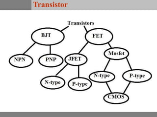
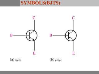
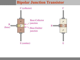
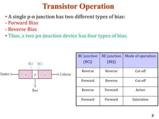
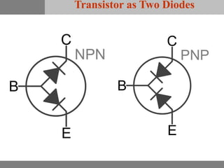
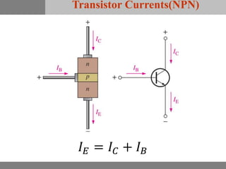
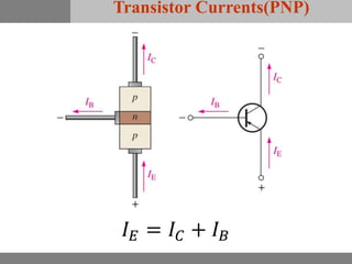
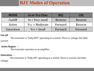
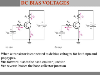
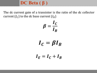
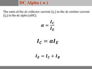
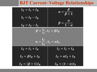
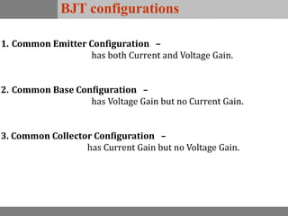
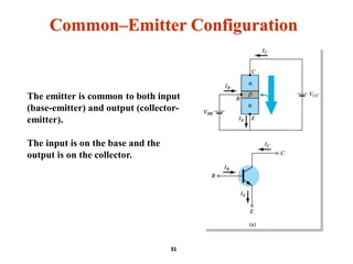
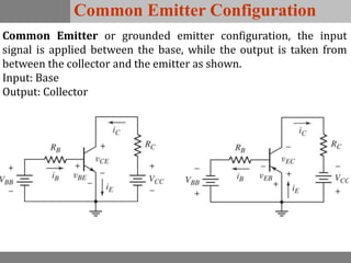
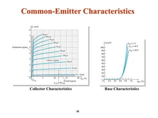
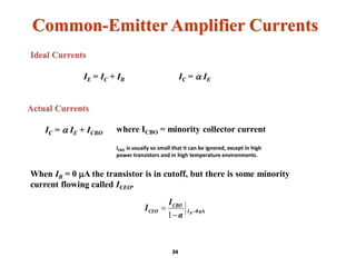
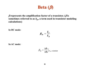
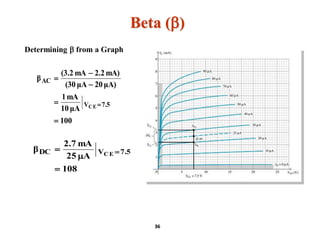
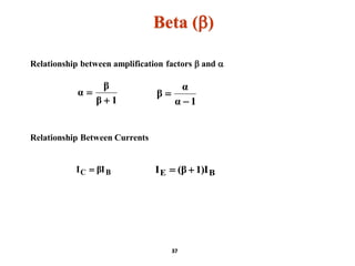
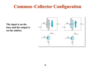
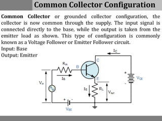
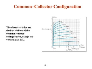
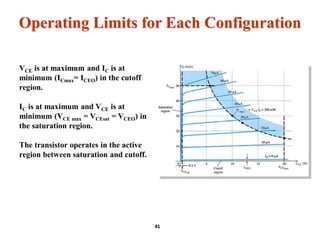
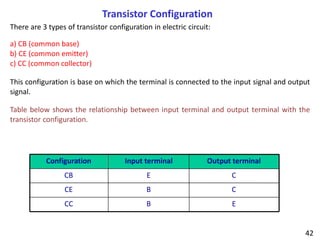
The three terminals of the FET are known as Gate, Drain, and Source.
It is a voltage controlled device, where the input voltage controls by the output current.
In FET current used to flow between the drain and the source terminal. And this current can be controlled by applying the voltage between the gate and the source terminal.
So this applied voltage generate the electric field within the device and by controlling these electric field we can control the flow of current through the device.
I presented this slid in my last presentation about bipolar junction transistor configuration.Now I'm sharing this with all of you guys it can be helpful for you.
Look at the beautiful view of forgiveness of mistakes.
Thank you
PN junction diode –structure, operation and V-I characteristics, diffusion and transient capacitance - Rectifiers – Half Wave and Full Wave Rectifier,– Display devices- LED, Laser diodes- Zener diodecharacteristics-Zener Reverse characteristics – Zener as regulator,TRANSISTORS, BJT, JFET, MOSFET- structure, operation, characteristics and Biasing UJT, Thyristor and IGBT Structure and characteristics,BJT small signal model – Analysis of CE, CB, CC amplifiers- Gain and frequency response –
MOSFET small signal model– Analysis of CS and Source follower – Gain and frequency response- High frequency analysis,BIMOS cascade amplifier, Differential amplifier – Common mode and Difference mode analysis – FET input stages – Single tuned amplifiers – Gain and frequency response – Neutralization methods, power amplifiers –Types (Qualitative analysis),Advantages of negative feedback – voltage / current, series , Shunt feedback –positive feedback – Condition for oscillations, phase shift – Wien bridge, Hartley, Colpitts and Crystal oscillators.
Here you find the information about Transistors. And know about
-> Type Of Transistor:
->Region of Transistor:
->P-N Junction Diodes
->Transistor application
->Transistor Connections
Limitation:
->Future of transistor:
The presentation covers Bipolar Junction Transistor: Construction, Operation, Transistor configurations and input / output characteristics; Common Base, Common Emitter, and Common Collector
The performance obtainable from a single-stage amplifier is often insufficient for many applications, hence several stages may be combined forming a multistage amplifier. These stages are connected in cascade, i.e. output of the first stage is connected to form input of second stage, whose output becomes input of third stage, and so on.
thank u
Hansraj MEENA
A Bipolar Junction Transistor is a three-terminal semiconductor device consisting of two p-n junctions which are able to amplify or magnify a signal. It is a current controlled device. The three terminals of the BJT are the base, the collector and the emitter. A BJT is a type of transistor that uses both electrons and holes as charge carriers
Student information management system project report ii.pdfKamal Acharya
Our project explains about the student management. This project mainly explains the various actions related to student details. This project shows some ease in adding, editing and deleting the student details. It also provides a less time consuming process for viewing, adding, editing and deleting the marks of the students.
Quality defects in TMT Bars, Possible causes and Potential Solutions.PrashantGoswami42
Maintaining high-quality standards in the production of TMT bars is crucial for ensuring structural integrity in construction. Addressing common defects through careful monitoring, standardized processes, and advanced technology can significantly improve the quality of TMT bars. Continuous training and adherence to quality control measures will also play a pivotal role in minimizing these defects.
Forklift Classes Overview by Intella PartsIntella Parts
Discover the different forklift classes and their specific applications. Learn how to choose the right forklift for your needs to ensure safety, efficiency, and compliance in your operations.
For more technical information, visit our website https://intellaparts.com
About
Indigenized remote control interface card suitable for MAFI system CCR equipment. Compatible for IDM8000 CCR. Backplane mounted serial and TCP/Ethernet communication module for CCR remote access. IDM 8000 CCR remote control on serial and TCP protocol.
• Remote control: Parallel or serial interface.
• Compatible with MAFI CCR system.
• Compatible with IDM8000 CCR.
• Compatible with Backplane mount serial communication.
• Compatible with commercial and Defence aviation CCR system.
• Remote control system for accessing CCR and allied system over serial or TCP.
• Indigenized local Support/presence in India.
• Easy in configuration using DIP switches.
Technical Specifications
Indigenized remote control interface card suitable for MAFI system CCR equipment. Compatible for IDM8000 CCR. Backplane mounted serial and TCP/Ethernet communication module for CCR remote access. IDM 8000 CCR remote control on serial and TCP protocol.
Key Features
Indigenized remote control interface card suitable for MAFI system CCR equipment. Compatible for IDM8000 CCR. Backplane mounted serial and TCP/Ethernet communication module for CCR remote access. IDM 8000 CCR remote control on serial and TCP protocol.
• Remote control: Parallel or serial interface
• Compatible with MAFI CCR system
• Copatiable with IDM8000 CCR
• Compatible with Backplane mount serial communication.
• Compatible with commercial and Defence aviation CCR system.
• Remote control system for accessing CCR and allied system over serial or TCP.
• Indigenized local Support/presence in India.
Application
• Remote control: Parallel or serial interface.
• Compatible with MAFI CCR system.
• Compatible with IDM8000 CCR.
• Compatible with Backplane mount serial communication.
• Compatible with commercial and Defence aviation CCR system.
• Remote control system for accessing CCR and allied system over serial or TCP.
• Indigenized local Support/presence in India.
• Easy in configuration using DIP switches.
Cosmetic shop management system project report.pdfKamal Acharya
Buying new cosmetic products is difficult. It can even be scary for those who have sensitive skin and are prone to skin trouble. The information needed to alleviate this problem is on the back of each product, but it's thought to interpret those ingredient lists unless you have a background in chemistry.
Instead of buying and hoping for the best, we can use data science to help us predict which products may be good fits for us. It includes various function programs to do the above mentioned tasks.
Data file handling has been effectively used in the program.
The automated cosmetic shop management system should deal with the automation of general workflow and administration process of the shop. The main processes of the system focus on customer's request where the system is able to search the most appropriate products and deliver it to the customers. It should help the employees to quickly identify the list of cosmetic product that have reached the minimum quantity and also keep a track of expired date for each cosmetic product. It should help the employees to find the rack number in which the product is placed.It is also Faster and more efficient way.
Welcome to WIPAC Monthly the magazine brought to you by the LinkedIn Group Water Industry Process Automation & Control.
In this month's edition, along with this month's industry news to celebrate the 13 years since the group was created we have articles including
A case study of the used of Advanced Process Control at the Wastewater Treatment works at Lleida in Spain
A look back on an article on smart wastewater networks in order to see how the industry has measured up in the interim around the adoption of Digital Transformation in the Water Industry.
Saudi Arabia stands as a titan in the global energy landscape, renowned for its abundant oil and gas resources. It's the largest exporter of petroleum and holds some of the world's most significant reserves. Let's delve into the top 10 oil and gas projects shaping Saudi Arabia's energy future in 2024.
Vaccine management system project report documentation..pdfKamal Acharya
The Division of Vaccine and Immunization is facing increasing difficulty monitoring vaccines and other commodities distribution once they have been distributed from the national stores. With the introduction of new vaccines, more challenges have been anticipated with this additions posing serious threat to the already over strained vaccine supply chain system in Kenya.
Water scarcity is the lack of fresh water resources to meet the standard water demand. There are two type of water scarcity. One is physical. The other is economic water scarcity.
CFD Simulation of By-pass Flow in a HRSG module by R&R Consult.pptxR&R Consult
CFD analysis is incredibly effective at solving mysteries and improving the performance of complex systems!
Here's a great example: At a large natural gas-fired power plant, where they use waste heat to generate steam and energy, they were puzzled that their boiler wasn't producing as much steam as expected.
R&R and Tetra Engineering Group Inc. were asked to solve the issue with reduced steam production.
An inspection had shown that a significant amount of hot flue gas was bypassing the boiler tubes, where the heat was supposed to be transferred.
R&R Consult conducted a CFD analysis, which revealed that 6.3% of the flue gas was bypassing the boiler tubes without transferring heat. The analysis also showed that the flue gas was instead being directed along the sides of the boiler and between the modules that were supposed to capture the heat. This was the cause of the reduced performance.
Based on our results, Tetra Engineering installed covering plates to reduce the bypass flow. This improved the boiler's performance and increased electricity production.
It is always satisfying when we can help solve complex challenges like this. Do your systems also need a check-up or optimization? Give us a call!
Work done in cooperation with James Malloy and David Moelling from Tetra Engineering.
More examples of our work https://www.r-r-consult.dk/en/cases-en/
2. What is a Transistor?
• Semiconductors: ability to change from
conductor to insulator
• Can either allow current or prohibit
current to flow
• Useful as a switch, but also as an amplifier
• Essential part of many technological
advances
A transistor is a semiconductor device
used to amplify and switch electronic
signals and electrical power.
3. Transistor Operation
With the external sources, VEE and VCC, connected as shown:
• The emitter-base junction is forward biased
• The base-collector junction is reverse biased
3
4. Currents in a Transistor
The collector current is comprised of two
currents:
BICIEI
minority
COI
majority
CICI
Emitter current is the sum of the collector and
base currents:
4
8. • A single p-n junction has two different types of bias:
- Forward Bias
- Reverse Bias
• Thus, a two pn-jnuction device has four types of bias.
SaturationForwardForward
ActiveForwardReverse
Cut-offReverseForward
Cut-offReverseReverse
Mode of operationBE junction
(BEJ)
BC junction
(BCJ)
8
Transistor Operation
9. BJT Construction
• The emitter layer is heavily doped, the base lightly
doped and collector only lightly doped.
• The doping of the sandwiched layer is considerably less
than the outer layers (typically 10:1 or less).
• Lower doping level decreases the conductivity of the
material by limiting the number of free electrons.
• The outer layers have widths much greater than the
sandwiched p- or n-type material. The ratio of the total
width to that of the central layer is 150:1.
10. JUNCTIONS
BASE-EMITTER JUNCTION(BEJ):
The pn junction joining the base region and the emitter region is
called the base-emitter junction
COLLECTOR-BASE JUNCTION(CBJ):
The pn junction joining the base region and the collector region
is called the collector-base junction
16. BJT Modes of Operation
MODE IB or VCE Char. BEJ CBJ
CutOff IB = Very small Reverse Reverse
Active VCE = Moderate Forward Reverse
Saturation VCE = Small Forward Forward
Cut-off –
The transistor is “Fully-OFF” operating as a switch. There is voltage, but little
current
Active Region –
The transistor operates as an amplifier
Saturation –
The transistor is “Fully-ON” operating as a switch. There is current, but little
voltage.
17. DC BIAS VOLTAGES
When a transistor is connected to dc bias voltages, for both npn and
pnp types,
VBB forward-biases the base-emitter junction
VCC reverse-biases the base-collector junction
18. DC Beta ( β )
𝑰 𝑬 = 𝑰 𝑪 + 𝑰 𝑩
The dc current gain of a transistor is the ratio of the dc collector
current (𝐼 𝐶) to the dc base current (𝐼 𝐵)
𝜷 =
𝑰 𝑪
𝑰 𝑩
𝑰 𝑪 = 𝜷𝑰 𝑩
19. DC Alpha ( α )
𝑰 𝑬 = 𝑰 𝑪 + 𝑰 𝑩
The ratio of the dc collector current (𝐼 𝐶) to the dc emitter current
(𝐼 𝐸) is the dc alpha (αDC).
𝜶 =
𝑰 𝑪
𝑰 𝑬
𝑰 𝑪 = 𝜶𝑰 𝑬
22. BJT configurations
1. Common Emitter Configuration –
has both Current and Voltage Gain.
2. Common Base Configuration –
has Voltage Gain but no Current Gain.
3. Common Collector Configuration –
has Current Gain but no Voltage Gain.
24. Common Base Configuration
Common Base or grounded base configuration, the BASE connection
is common to both the input signal AND the output signal with the
input signal being applied between the base and the emitter
terminals. The corresponding output signal is taken from between
the base and the collector terminals
Input: Emitter
Output: Collector
26. This graph demonstrates
the output current (IC) to
an output voltage (VCB) for
various levels of input
current (IE).
Common-Base Amplifier
Output Characteristics
26
27. Operating Regions
• Active – Operating range of the
amplifier.
• Cutoff – The amplifier is basically
off. There is voltage, but little
current.
• Saturation – The amplifier is full on.
There is current, but little voltage.
27
29. Ideally: a = 1
In reality: a is between 0.9 and 0.998
Alpha (a)
Alpha (a) is the ratio of IC to IE :
EI
CI
α dc
Alpha (a) in the AC mode:
EI
CI
α
Δ
Δ
ac
29
31. Common–Emitter Configuration
The emitter is common to both input
(base-emitter) and output (collector-
emitter).
The input is on the base and the
output is on the collector.
31
32. Common Emitter Configuration
Common Emitter or grounded emitter configuration, the input
signal is applied between the base, while the output is taken from
between the collector and the emitter as shown.
Input: Base
Output: Collector
34. Common-Emitter Amplifier Currents
Ideal Currents
IE = IC + IB IC = a IE
Actual Currents
IC = a IE + ICBO
When IB = 0 A the transistor is in cutoff, but there is some minority
current flowing called ICEO.
μA0
BI
CBO
CEO
α
I
I
1
where ICBO = minority collector current
34
ICBO is usually so small that it can be ignored, except in high
power transistors and in high temperature environments.
35. Beta ()
In DC mode:
In AC mode:
represents the amplification factor of a transistor. ( is
sometimes referred to as hfe, a term used in transistor modeling
calculations)
B
C
I
I
β dc
constantac
CEV
B
C
I
I
35
36. Determining from a Graph
Beta ()
108
A25
mA2.7
β 7.5VDC CE
100
μA10
mA1
μA)20μA(30
mA)2.2mA(3.2
β
7.5V
AC
CE
36
37. Relationship between amplification factors and a
1β
β
α
1α
α
β
Beta ()
Relationship Between Currents
BC βII BE 1)I(βI
37
39. Common Collector Configuration
Common Collector or grounded collector configuration, the
collector is now common through the supply. The input signal is
connected directly to the base, while the output is taken from the
emitter load as shown. This type of configuration is commonly
known as a Voltage Follower or Emitter Follower circuit.
Input: Base
Output: Emitter
41. VCE is at maximum and IC is at
minimum (ICmax= ICEO) in the cutoff
region.
IC is at maximum and VCE is at
minimum (VCE max = VCEsat = VCEO) in
the saturation region.
The transistor operates in the active
region between saturation and cutoff.
Operating Limits for Each Configuration
41
42. There are 3 types of transistor configuration in electric circuit:
a) CB (common base)
b) CE (common emitter)
c) CC (common collector)
This configuration is base on which the terminal is connected to the input signal and output
signal.
Table below shows the relationship between input terminal and output terminal with the
transistor configuration.
EBCC
CBCE
CECB
Output terminalInput terminalConfiguration
42
Transistor Configuration
43. Characteristics of the Transistor Configurations
Characteristic
Common
Base
Common
Emitter
Common
Collector
Input Impedance Low Medium High
Output
Impedance
Very High High Low
Phase Angle 0o 180o 0o
Voltage Gain High Medium Low
Current Gain Low Medium High
Power Gain Low Very High Medium