Download as PDF, PPTX
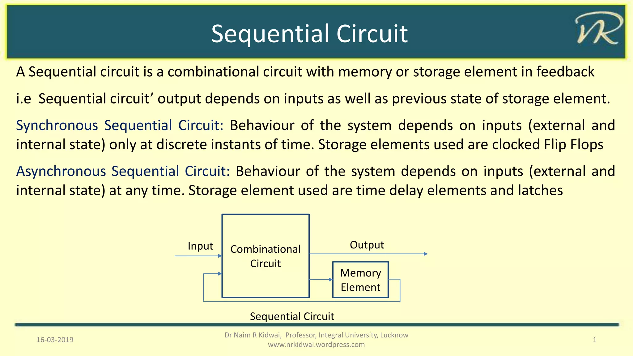
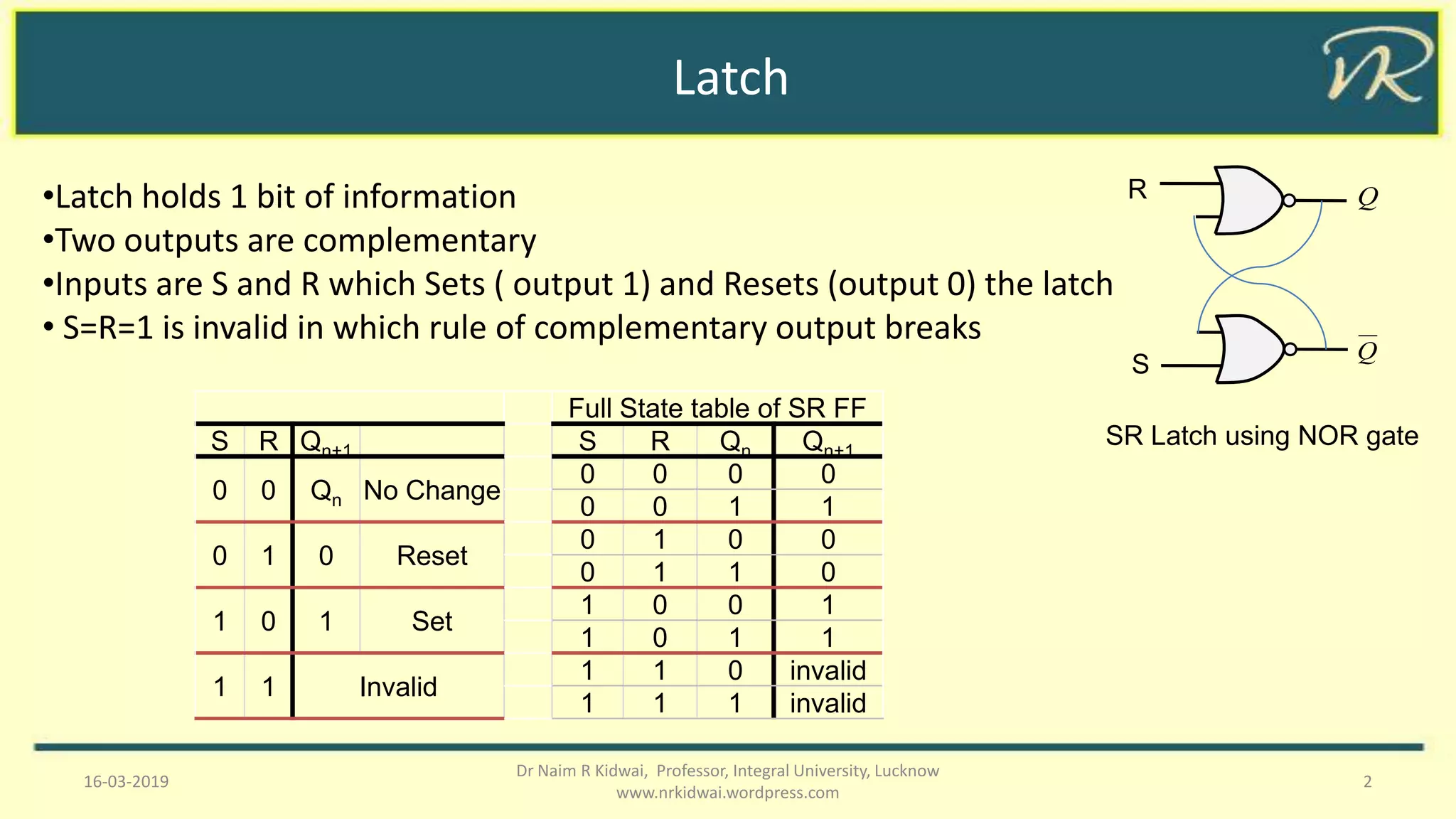
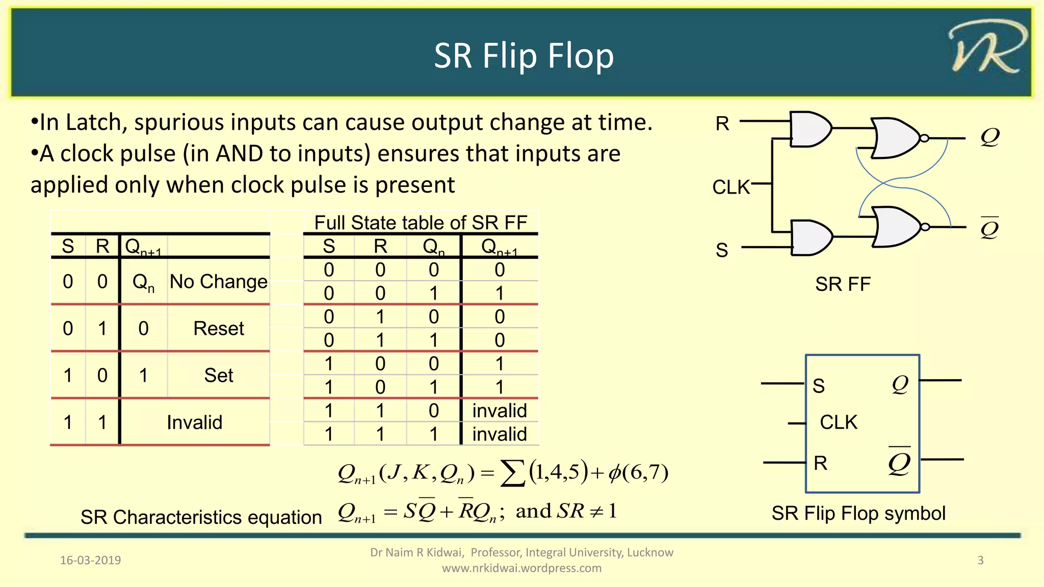
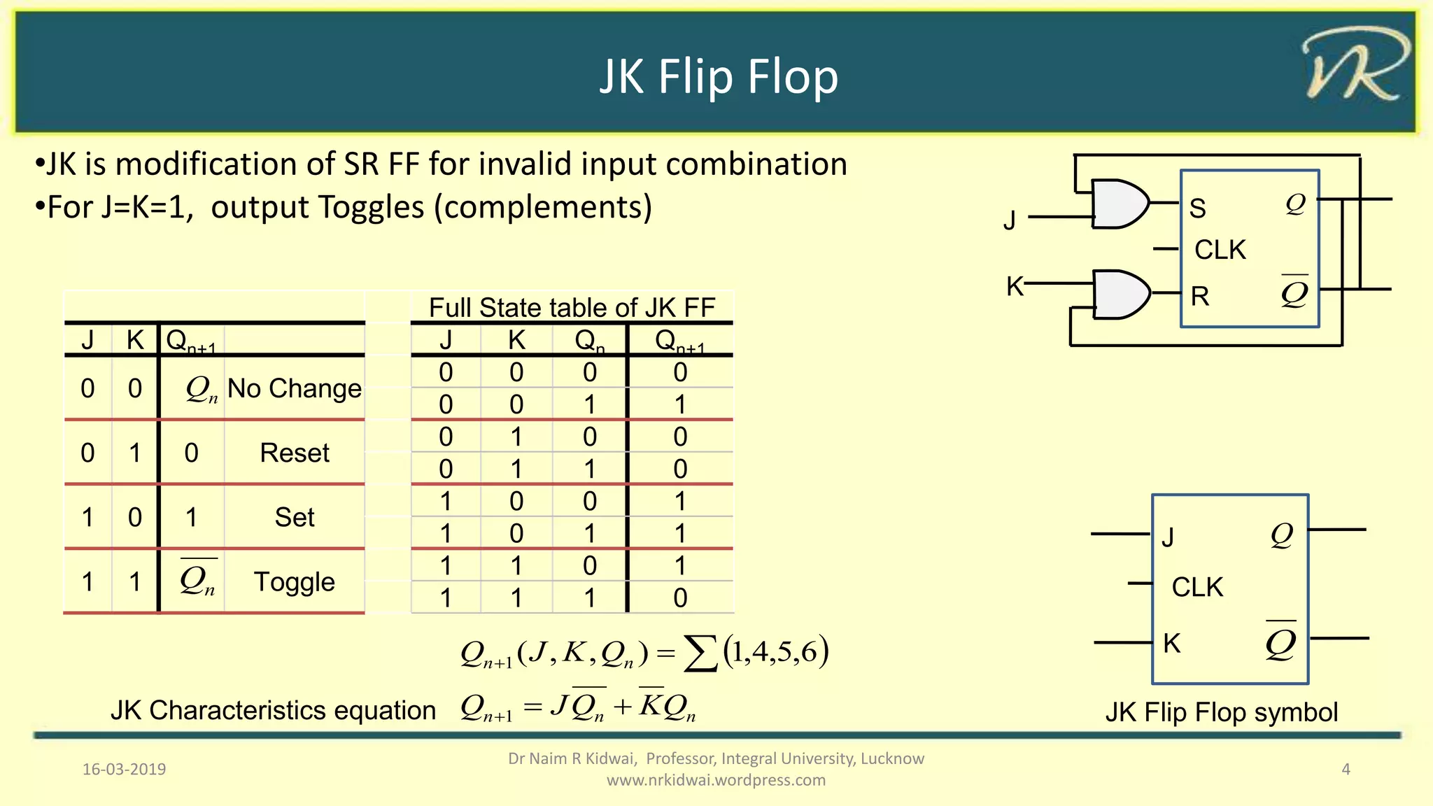
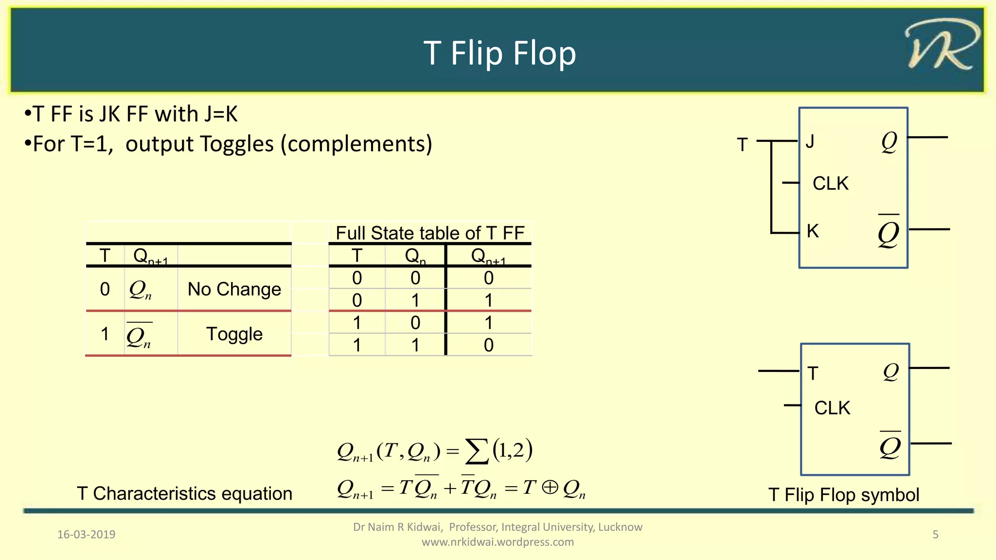
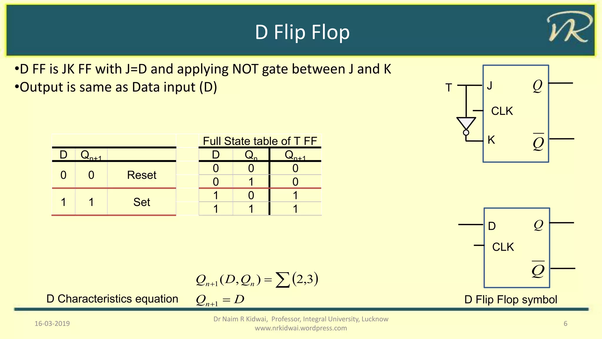
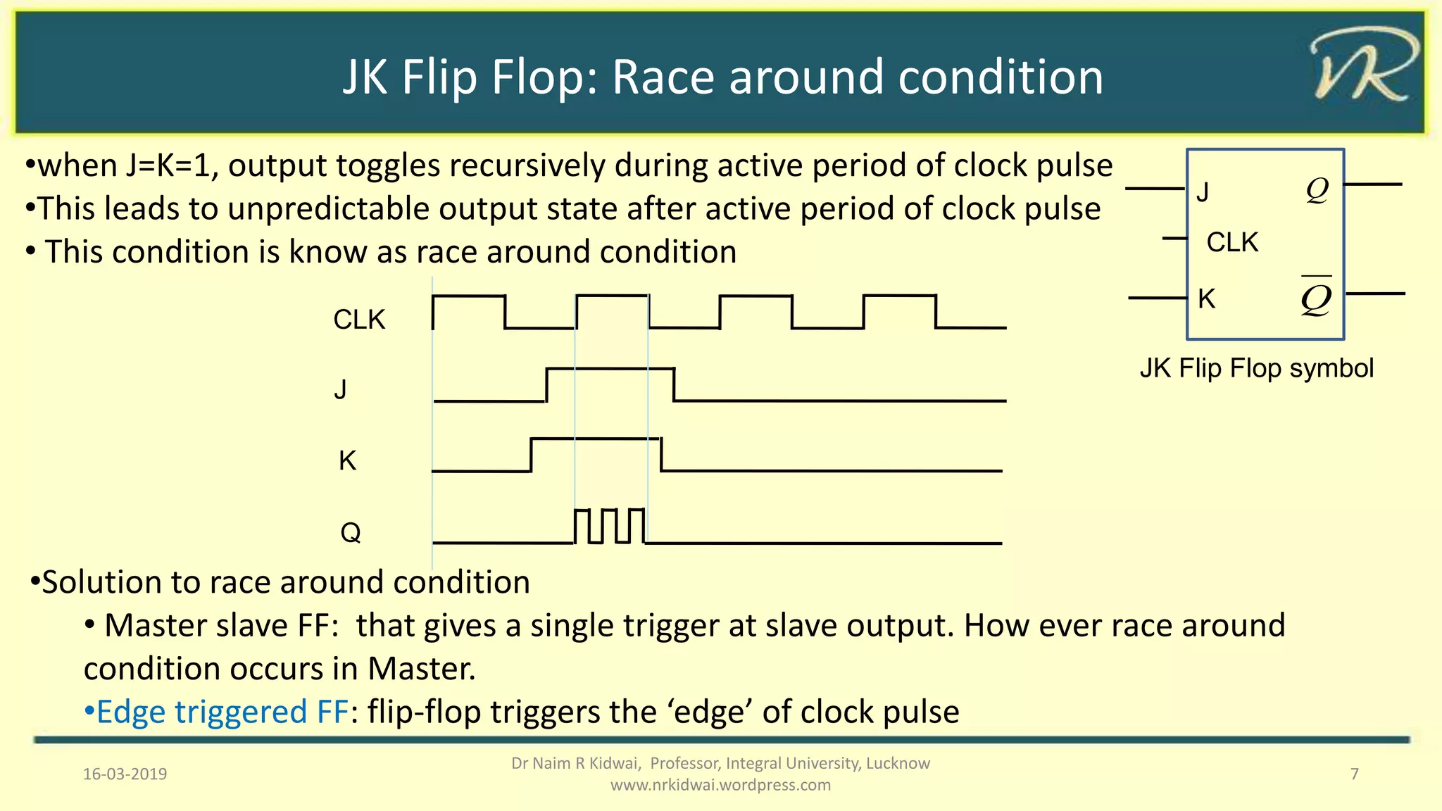
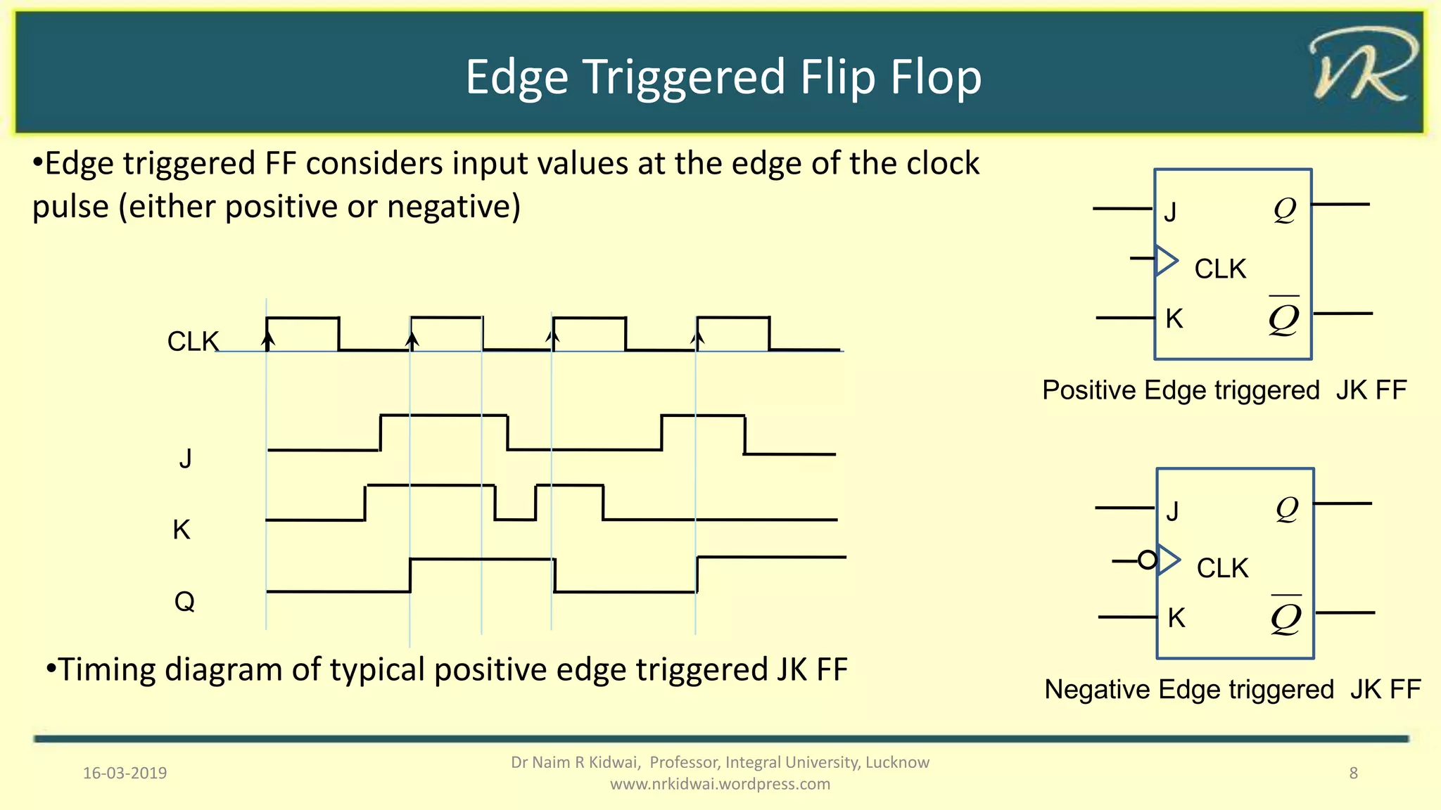
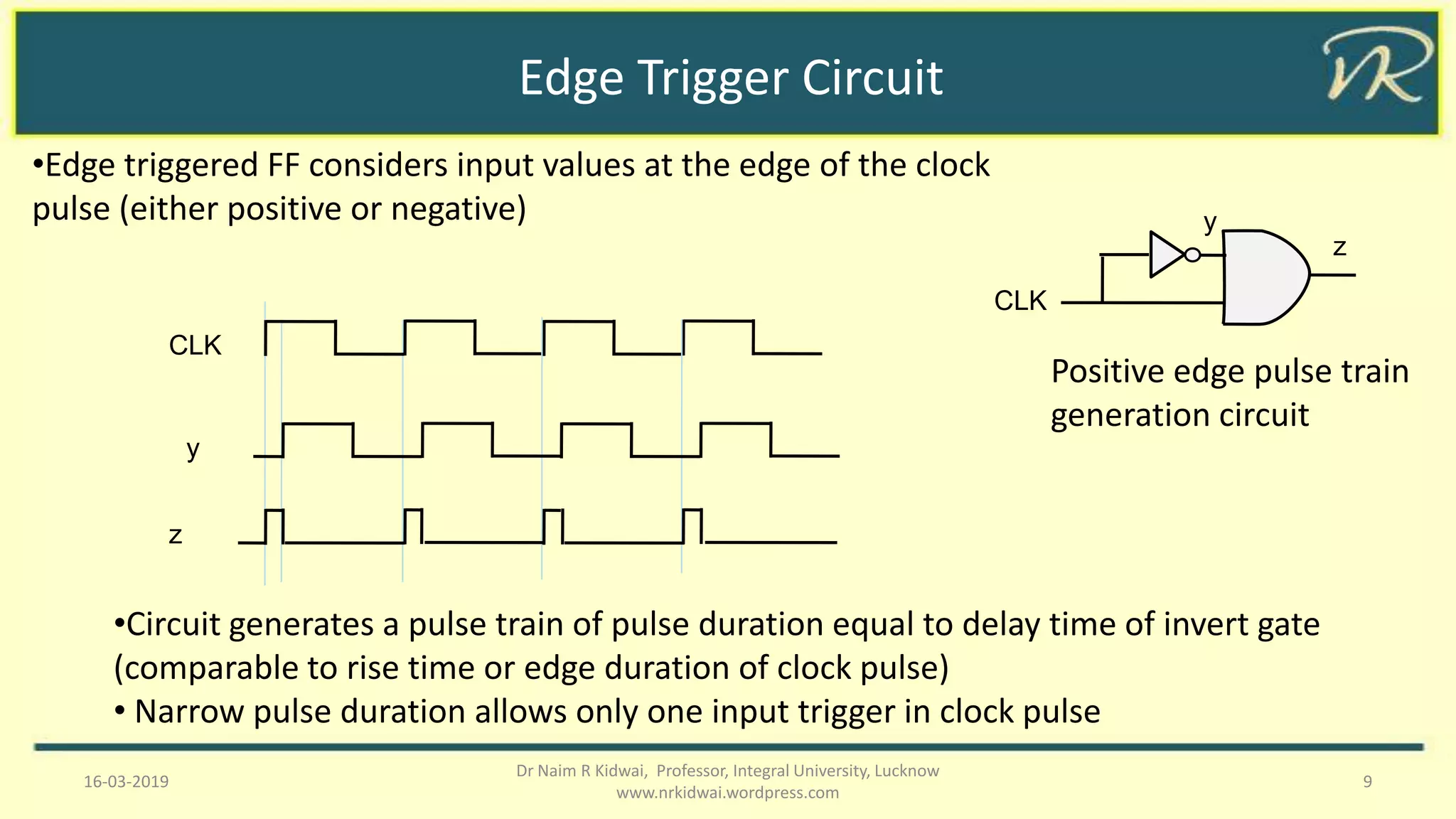
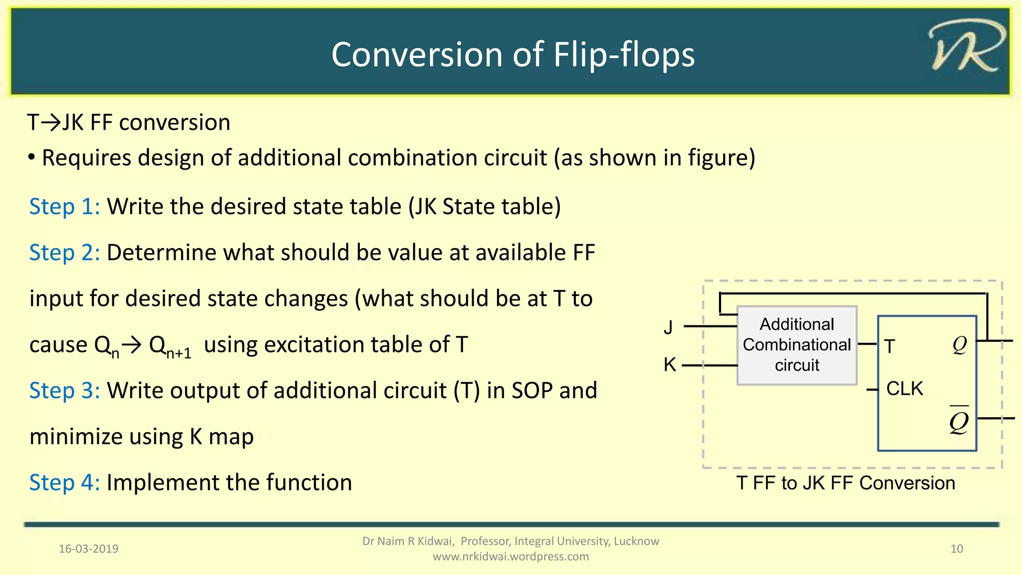
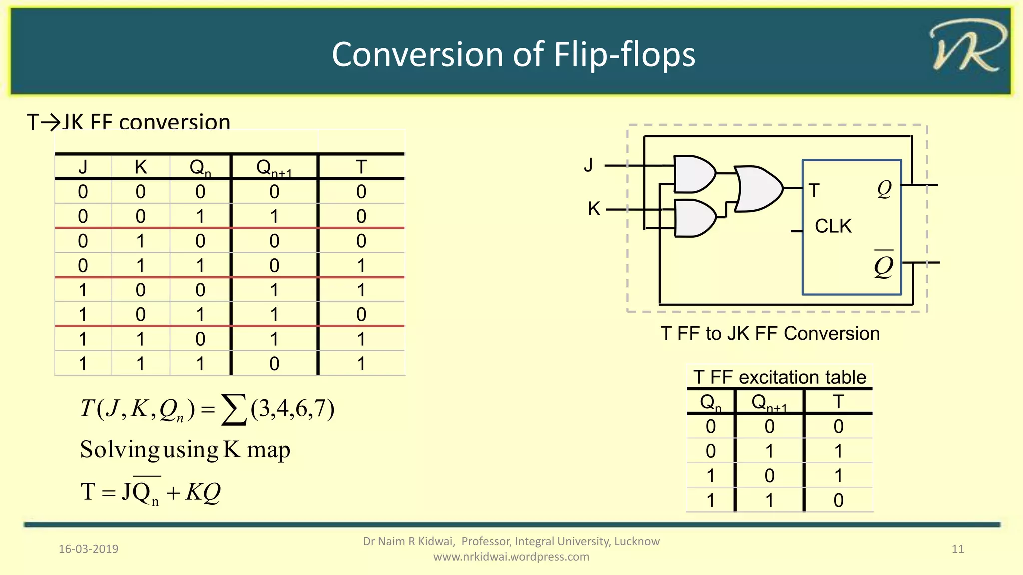

This document discusses sequential circuits, distinguishing between synchronous and asynchronous types, and details various flip-flops including SR, JK, T, and D flip-flops. It covers their behaviors, state tables, and issues such as race conditions, alongside solutions like master-slave and edge-triggered flip-flops. The document also explains the conversion processes between different flip-flop types and their excitation tables.