Downloaded 2,059 times
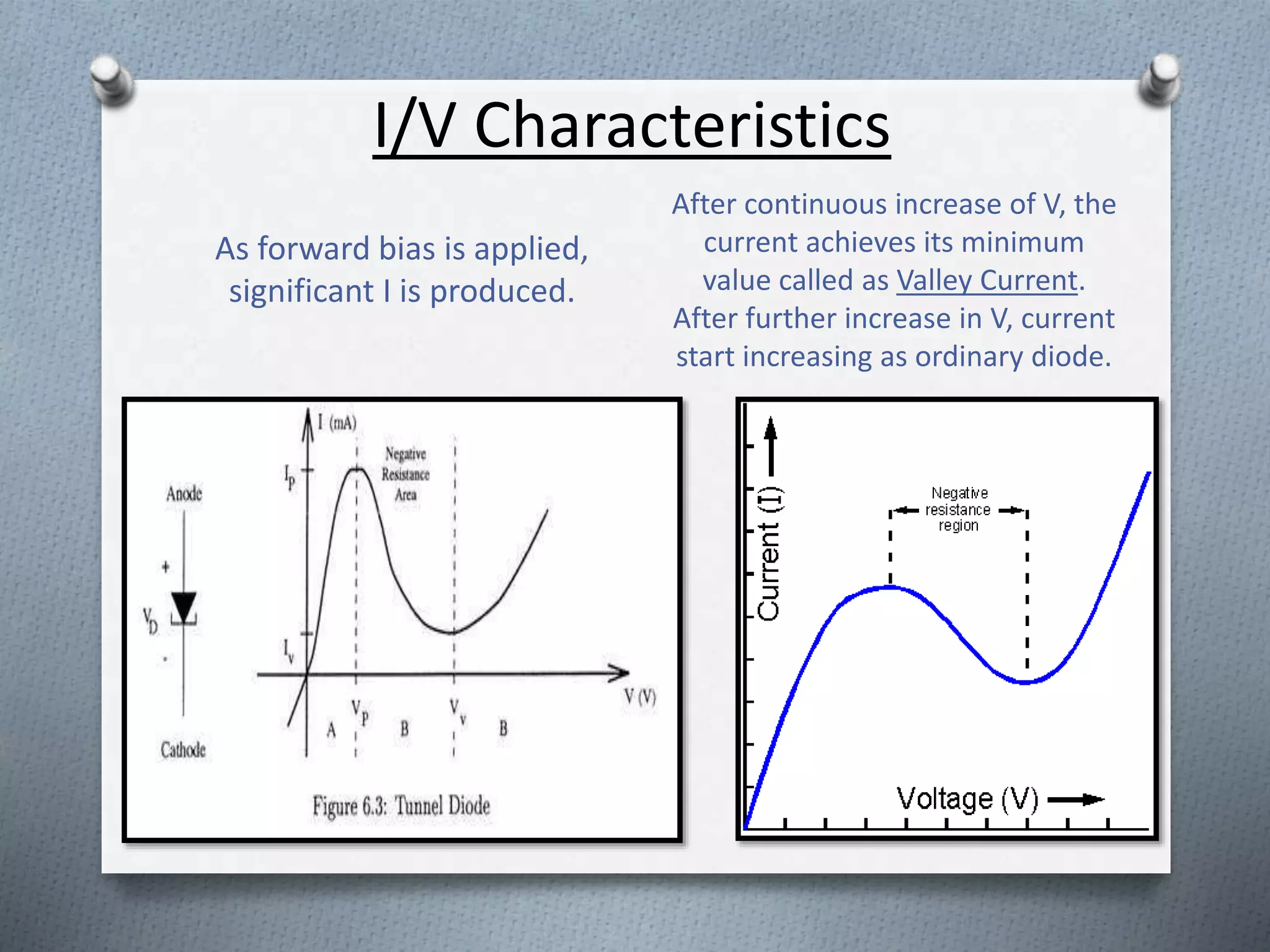


Tunnel diodes are heavily doped PN junction diodes that exhibit negative resistance. They were invented in 1958 by Dr. Leo Esaki and operate based on the quantum mechanical principle of tunneling. When forward biased, the current initially increases with voltage but then decreases as the voltage is further increased, demonstrating the unique property of negative resistance. Tunnel diodes find application in ultrafast switching, memory storage, satellite communication equipment, and oscillators due to their negative resistance characteristic.
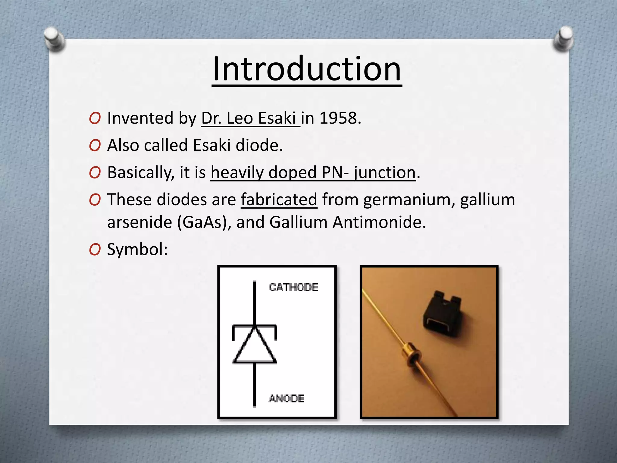
Tunnel diodes, invented by Dr. Leo Esaki in 1958, are heavily doped PN-junctions made from germanium and GaAs.
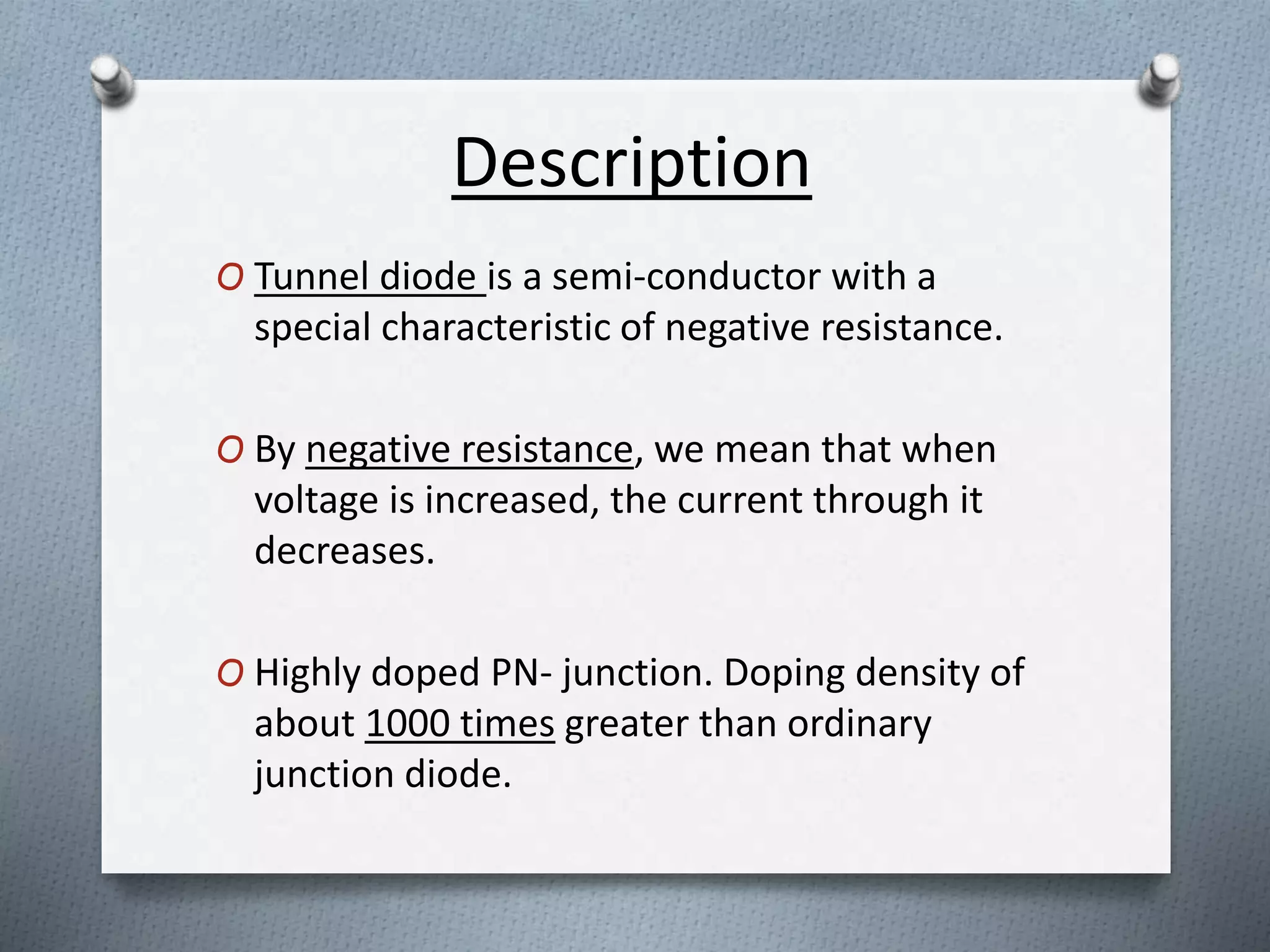
Tunnel diodes feature negative resistance where current decreases as voltage increases due to high doping.
Heavy doping reduces depletion width, reverse breakdown voltage, and allows conduction across reverse voltages.
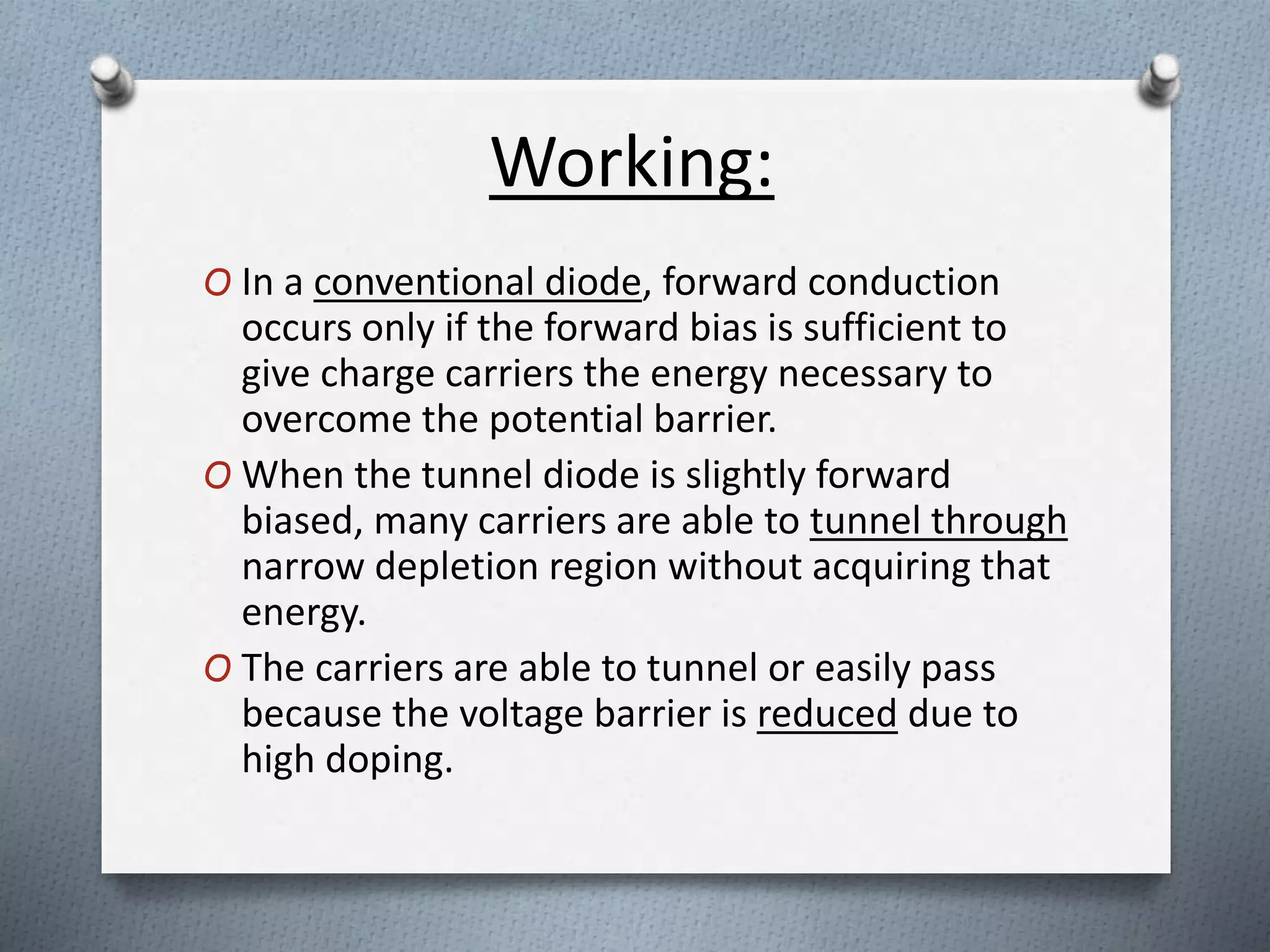
Tunnel diode operation relies on tunneling, enabling electron movement across barriers without voltage.
In a tunnel diode, electrons can tunnel through a narrow depletion region without high energy.
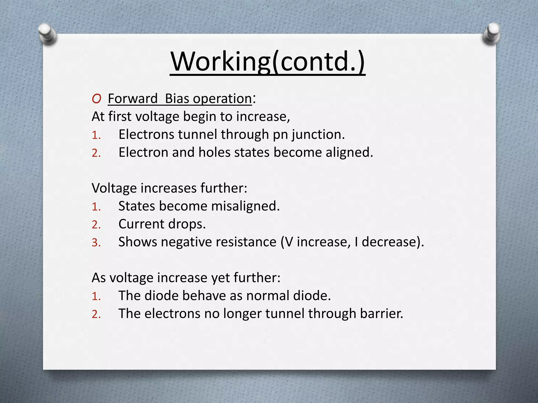
Initially, electrons tunnel easily at low voltage, but at higher voltages, the current drops displaying negative resistance.
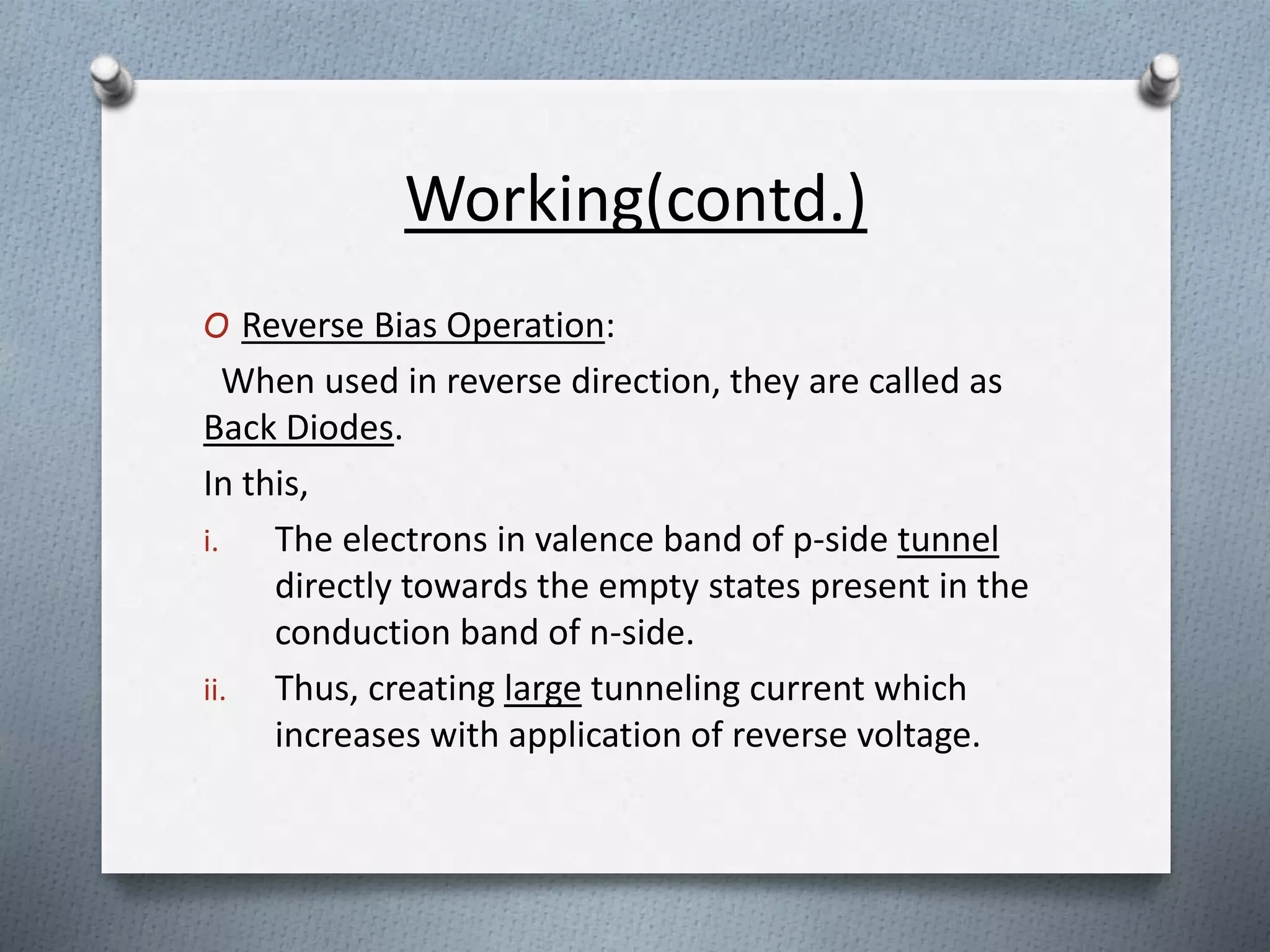
In reverse bias, electrons tunnel creating significant current, pointing to its distinct back diode behavior.
When forward bias increases, current shows a valley current followed by normal diode behavior.
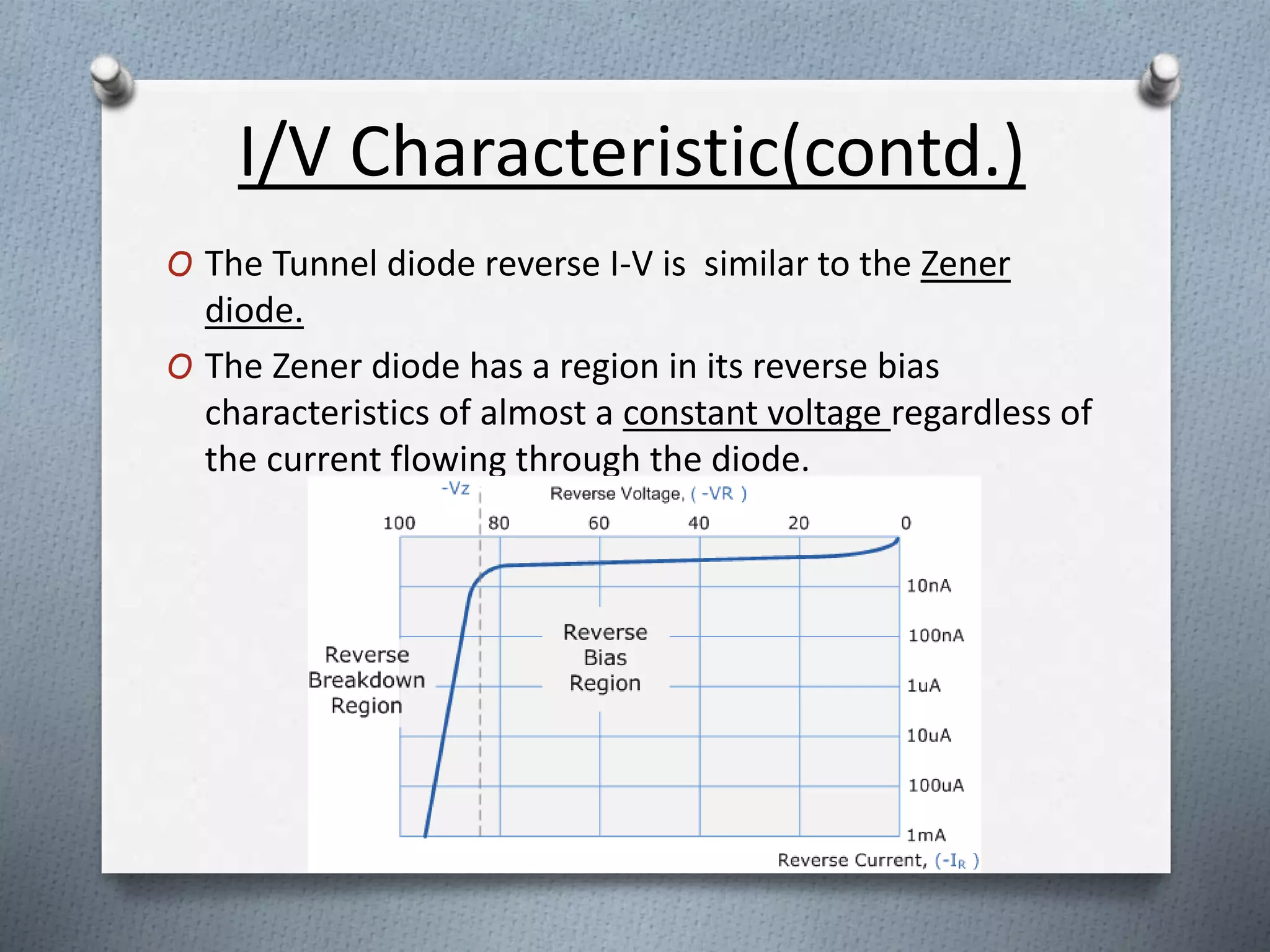
Tunnel diode’s reverse I-V characteristics resemble Zener diodes with constant voltage regions.
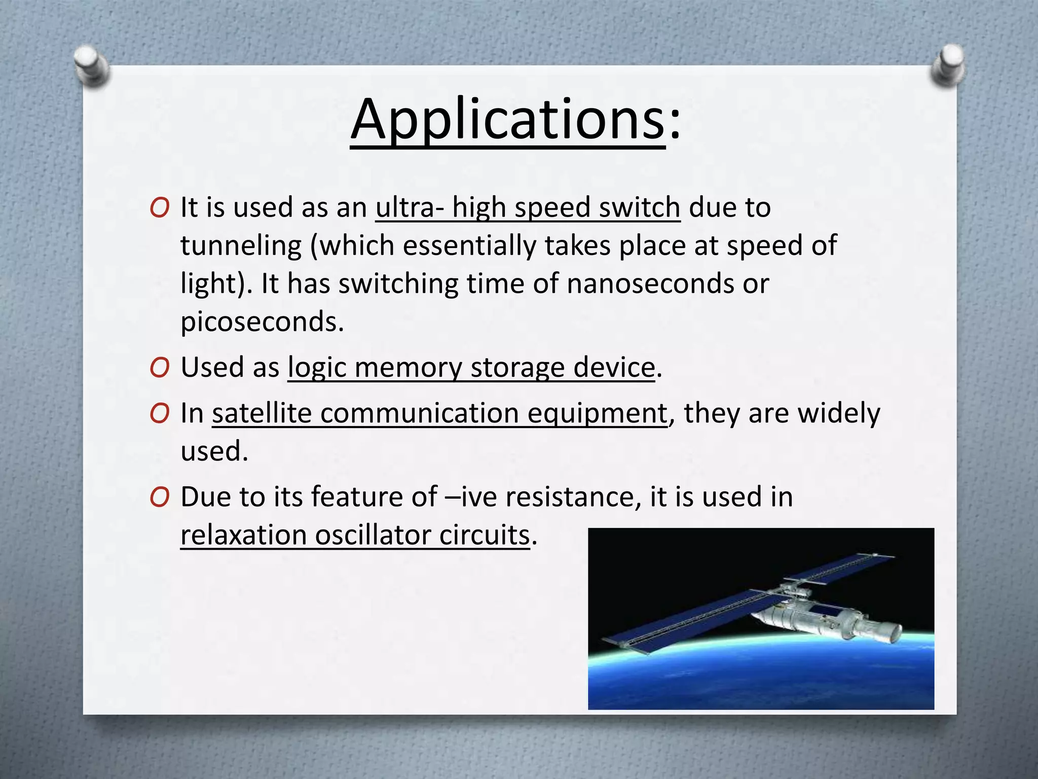
Used as high-speed switches, memory devices, and in satellite equipment due to tunneling properties.
Resistant to magnetic fields and high temperatures, they're utilized in military tech and low-power FM receivers.


![Tunnel_Diode[1].pdffdkjvnfvnfvkgvnjgrjvrgjbbjg](https://cdn.slidesharecdn.com/ss_thumbnails/tunneldiode1-241023150339-31eb82ff-thumbnail.jpg?width=640&height=640&fit=bounds)


