Downloaded 265 times


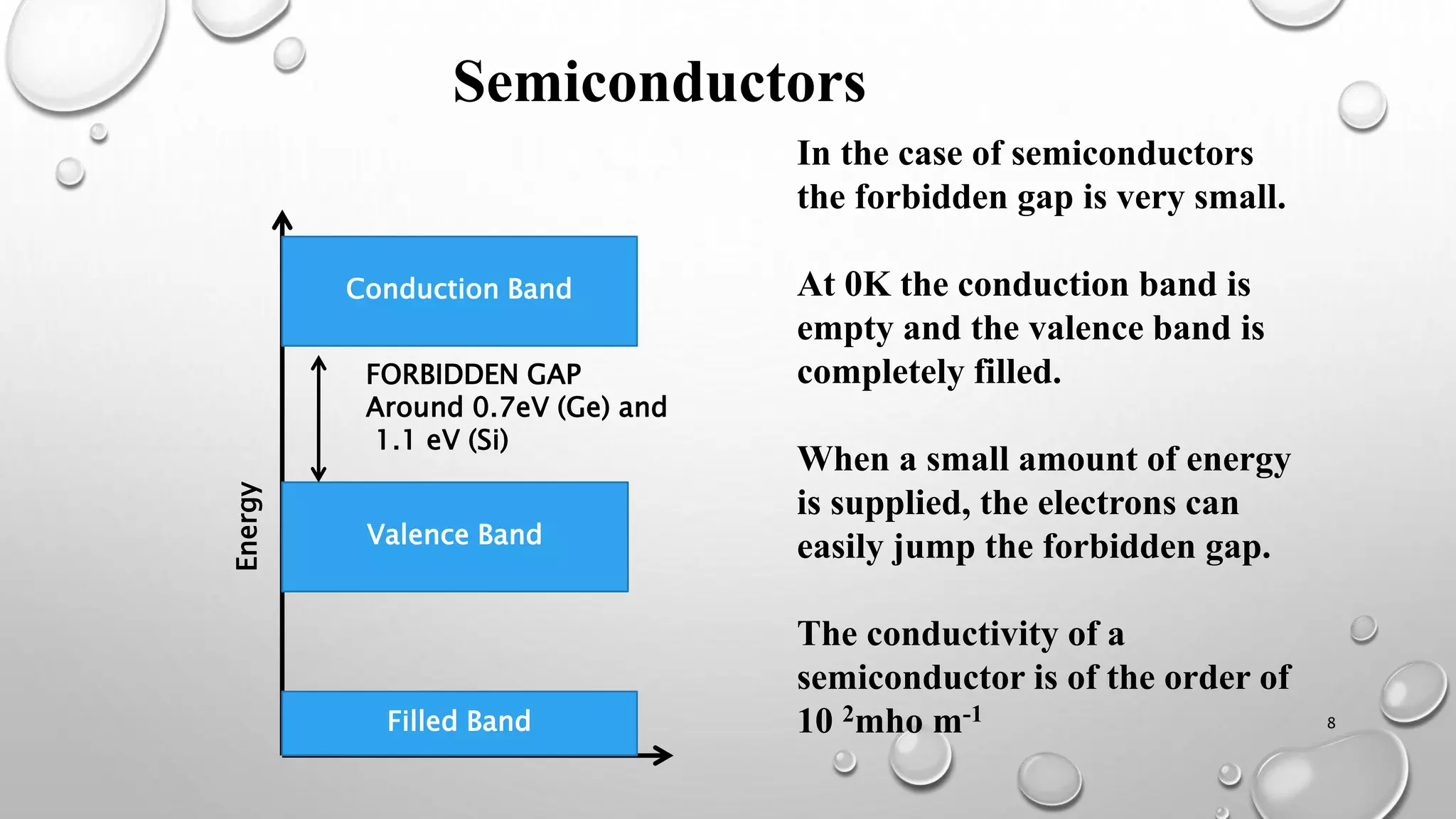

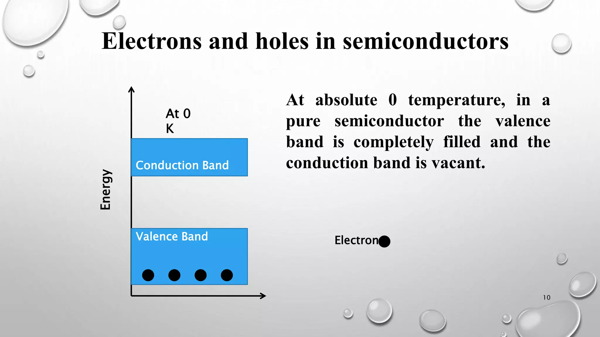
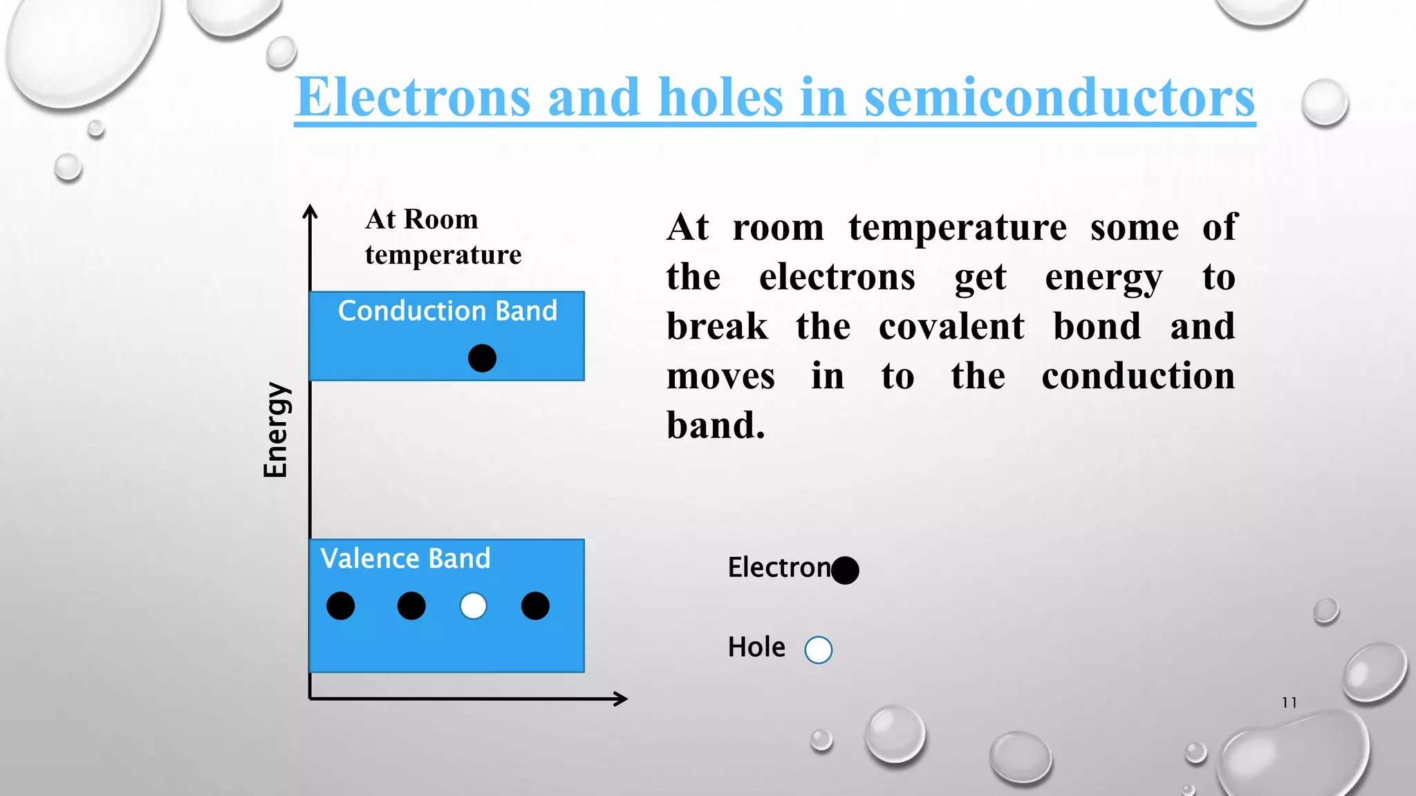


This document discusses semiconductors and their properties. Semiconductors have resistivity between good conductors and insulators, around 10-2 to 104 ohm meters at room temperature. In semiconductors, there is a small forbidden gap between the valence band and conduction band of around 0.7-1.1 electronvolts. This small gap means electrons can move between bands with only a small amount of energy, allowing semiconductors to conduct electricity. In contrast, insulators have a large forbidden gap over 3 electronvolts, while conductors have no gap between bands.


