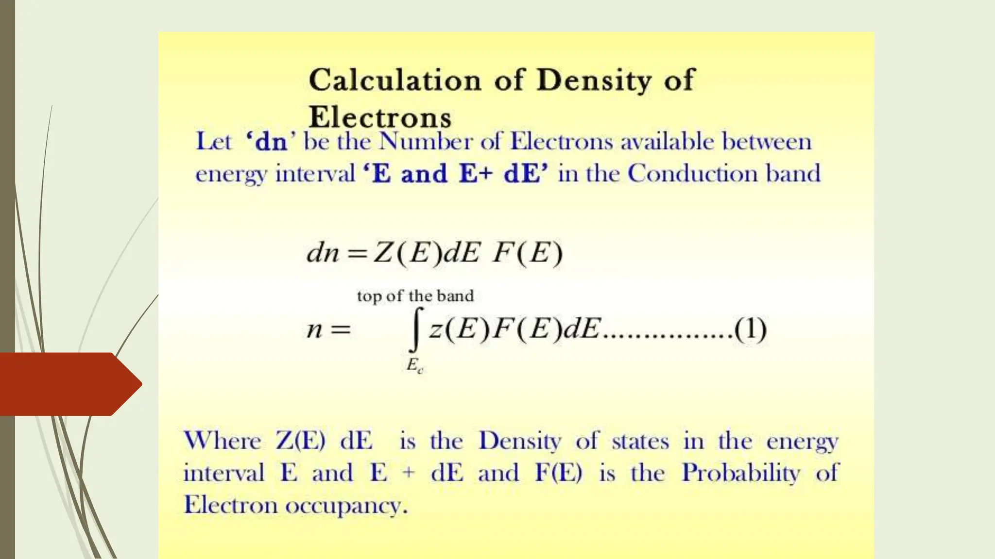
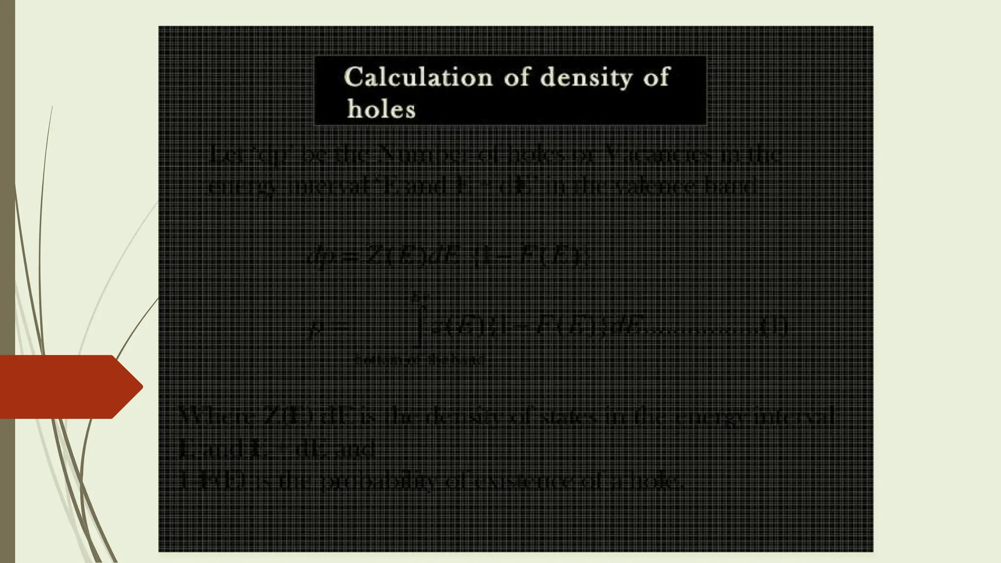
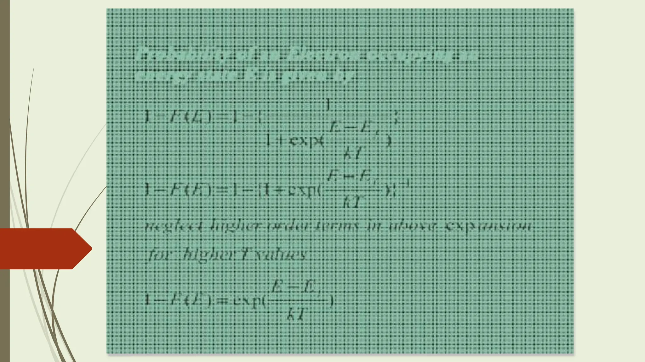
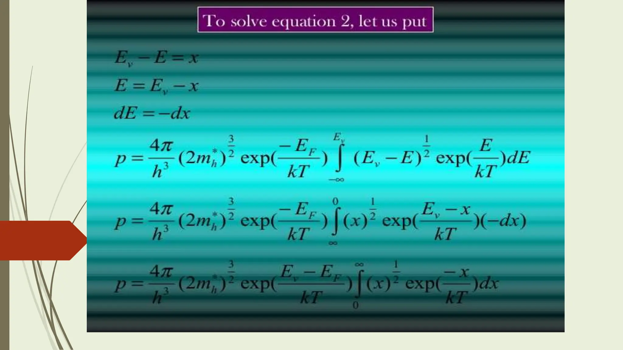
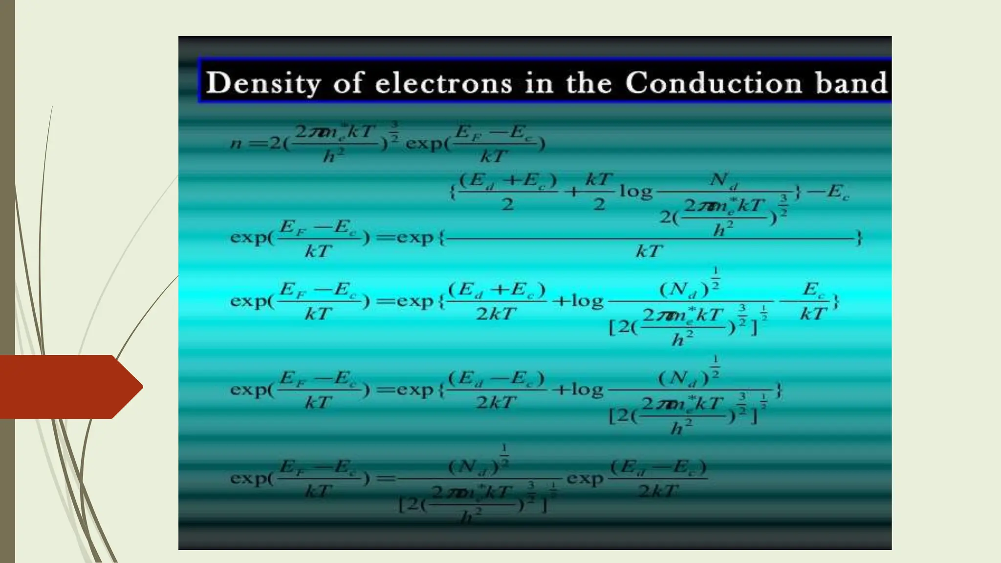
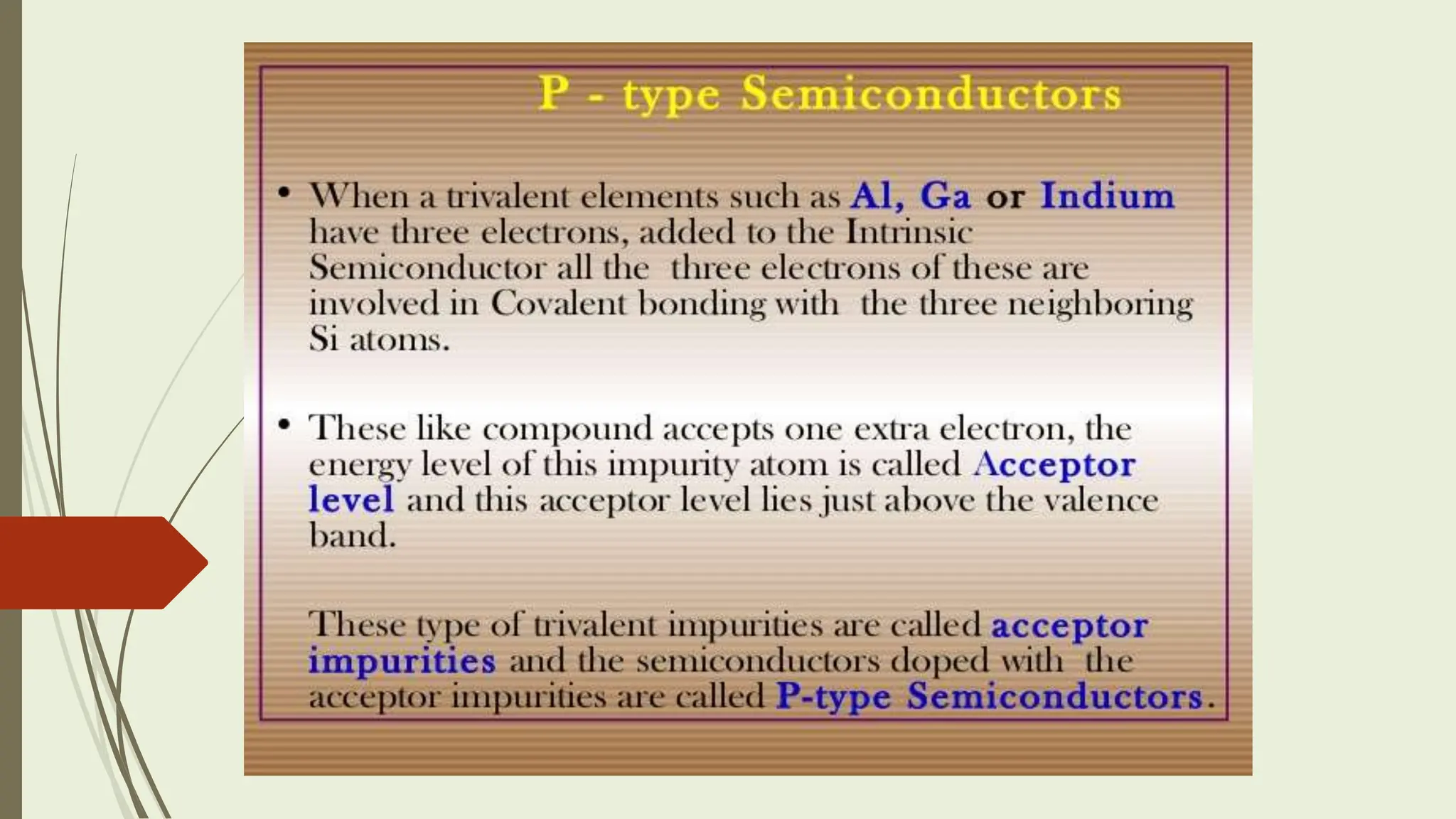
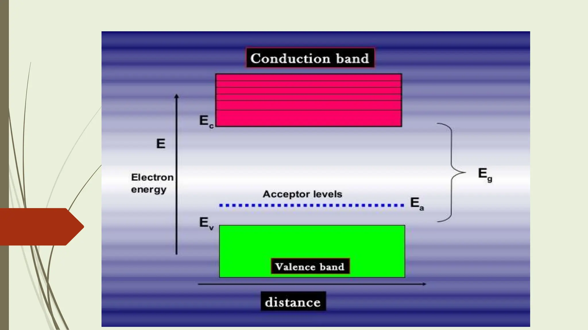
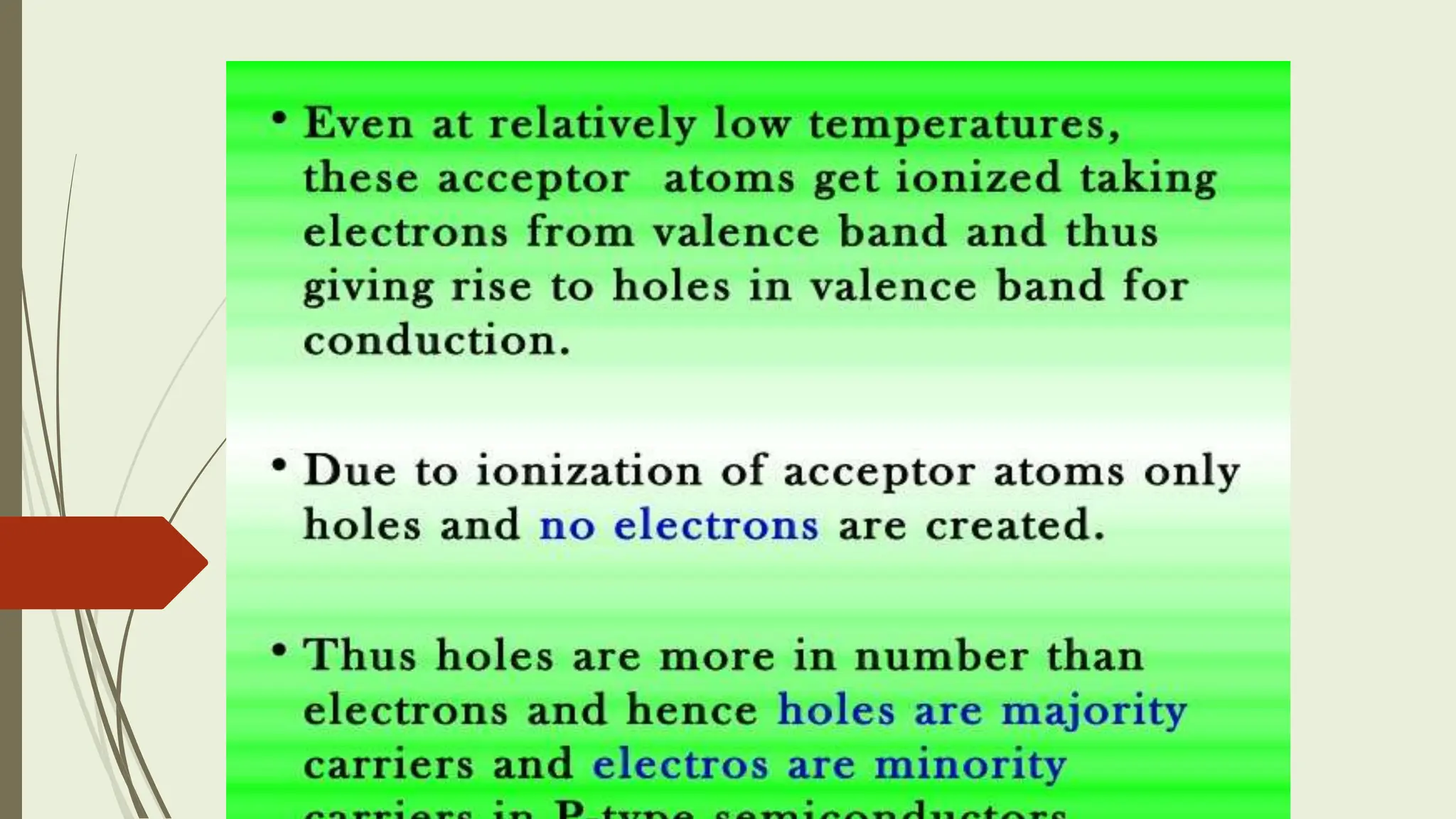
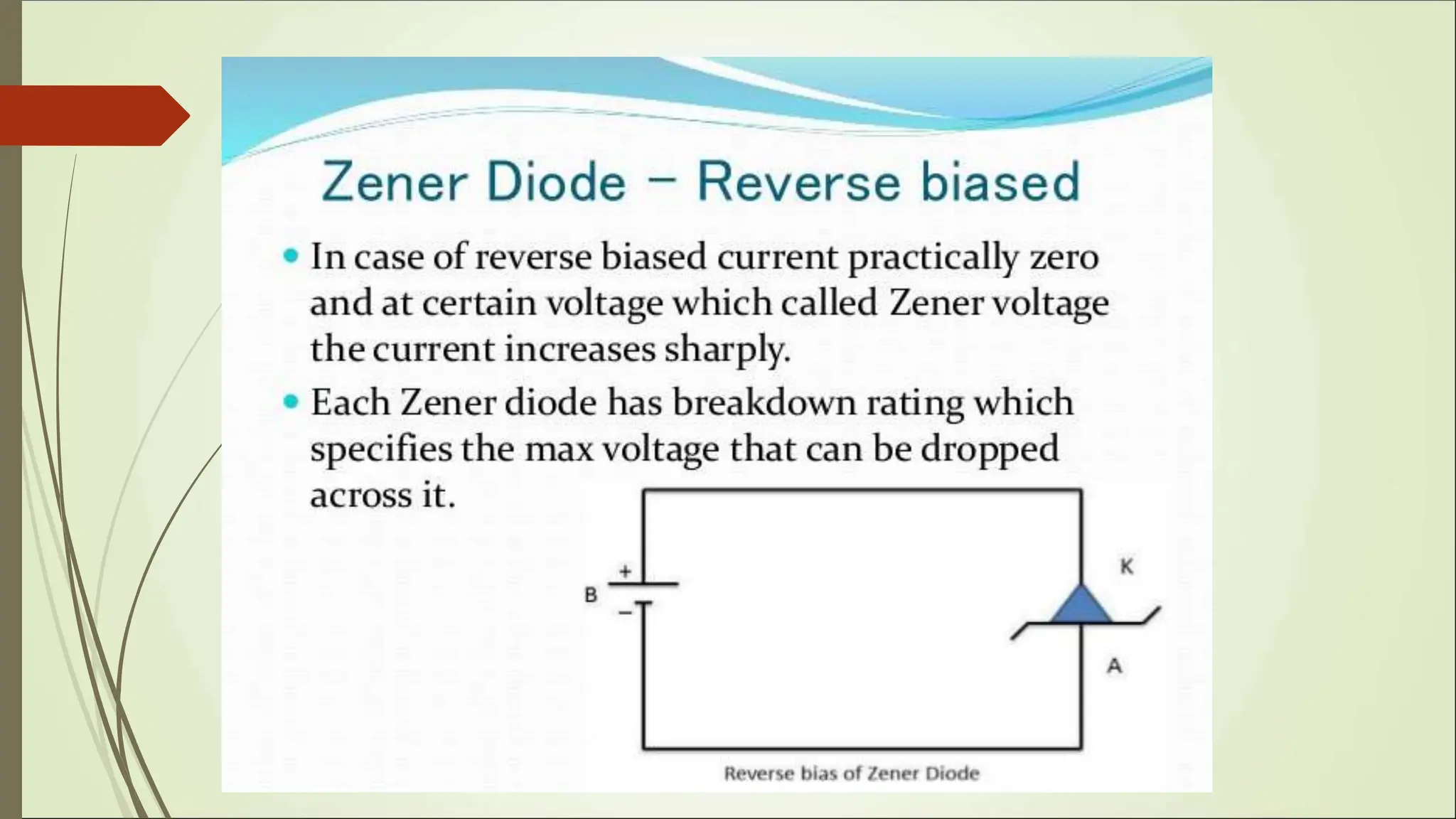
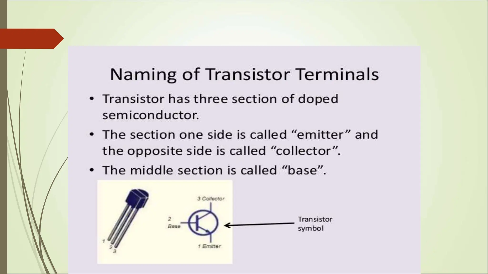
The document discusses the physics of PN junction diodes. It describes:
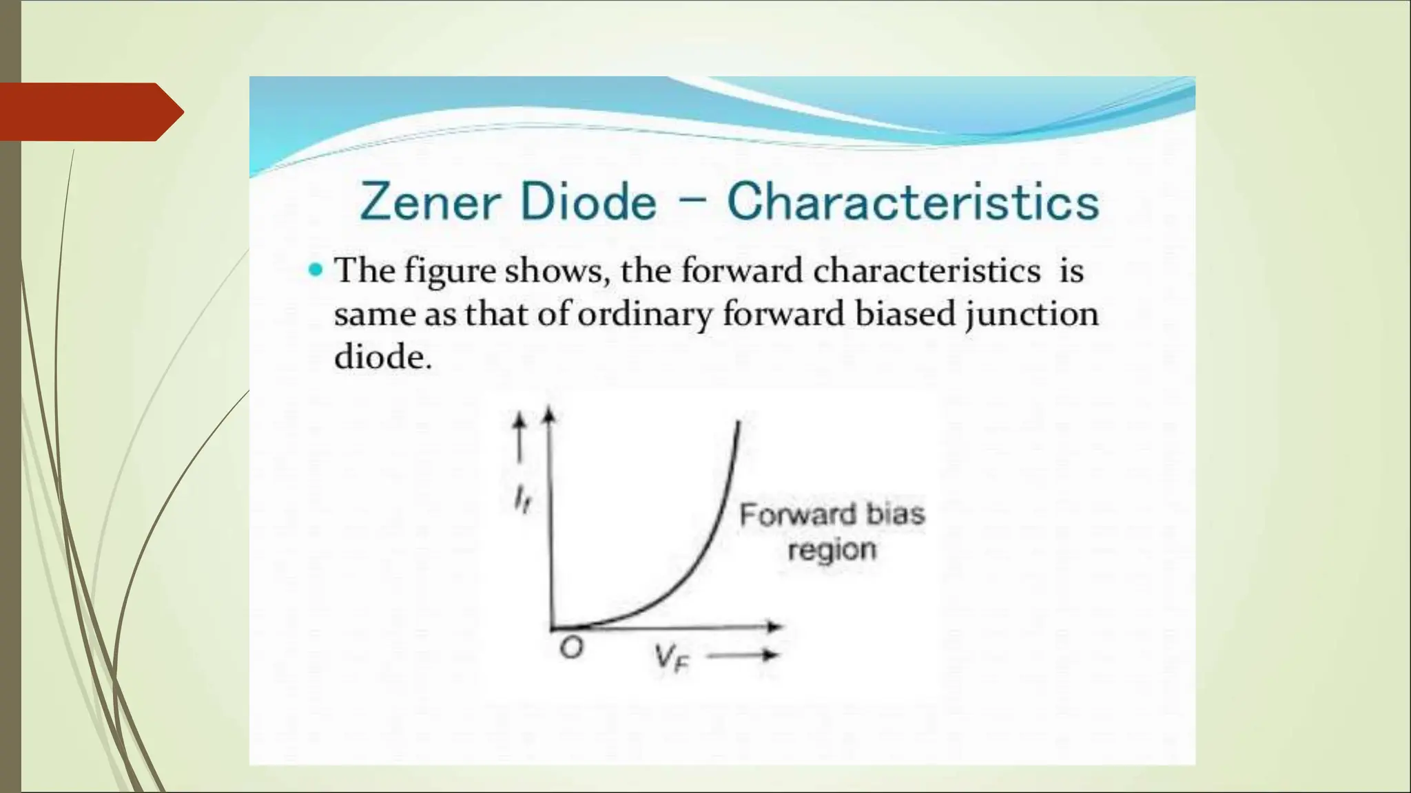
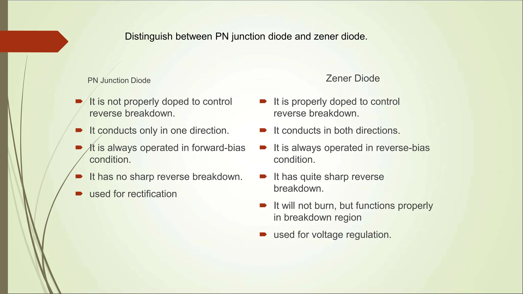
1. Forward and reverse biasing of a PN junction diode. In forward bias, the depletion region width decreases allowing carrier flow. In reverse bias, a small saturation current flows.
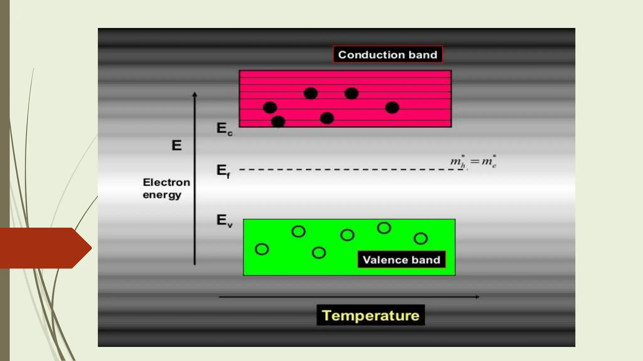
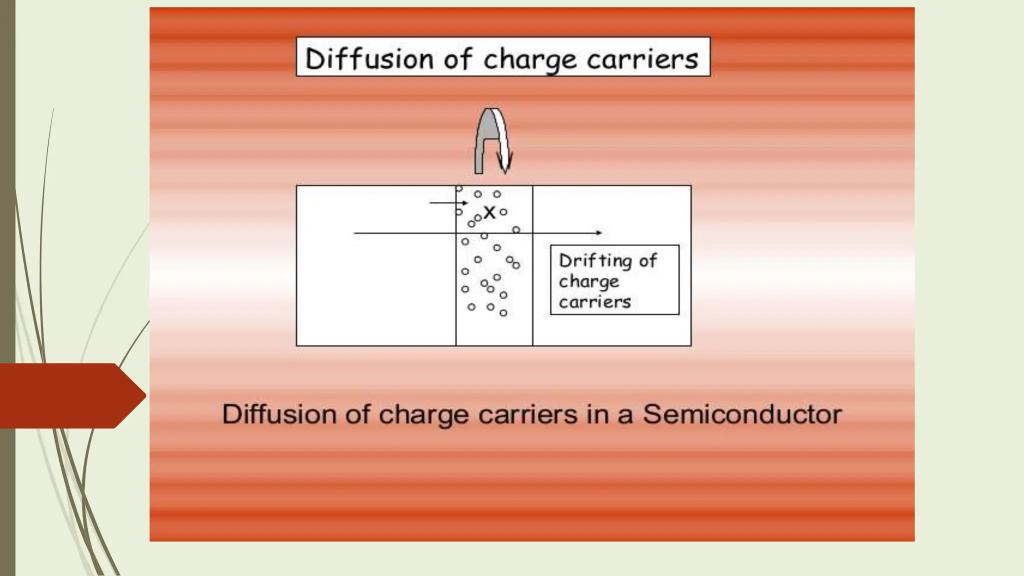
2. The formation of a depletion region at the PN junction due to diffusion of electrons and holes. This creates an electric field that opposes further diffusion.
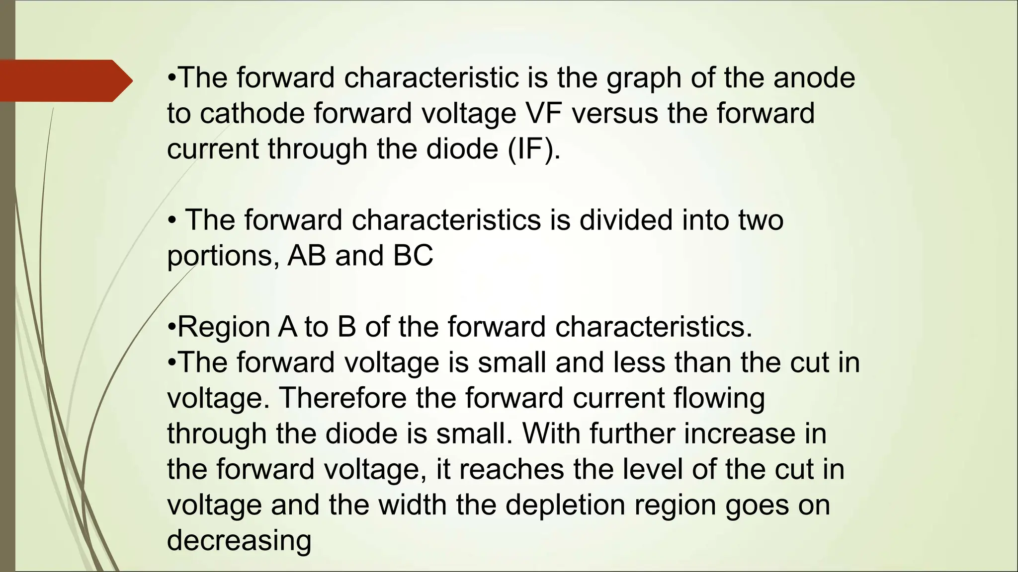
3. Key characteristics of a PN junction diode including cut-in voltage, depletion layer, static resistance, and avalanche breakdown under high reverse voltages.


![The Bermuda Triangle Mystery 1[1].pptx](https://cdn.slidesharecdn.com/ss_thumbnails/thebermudatrianglemystery11-231231140550-555c31eb-thumbnail.jpg?width=640&height=640&fit=bounds)


