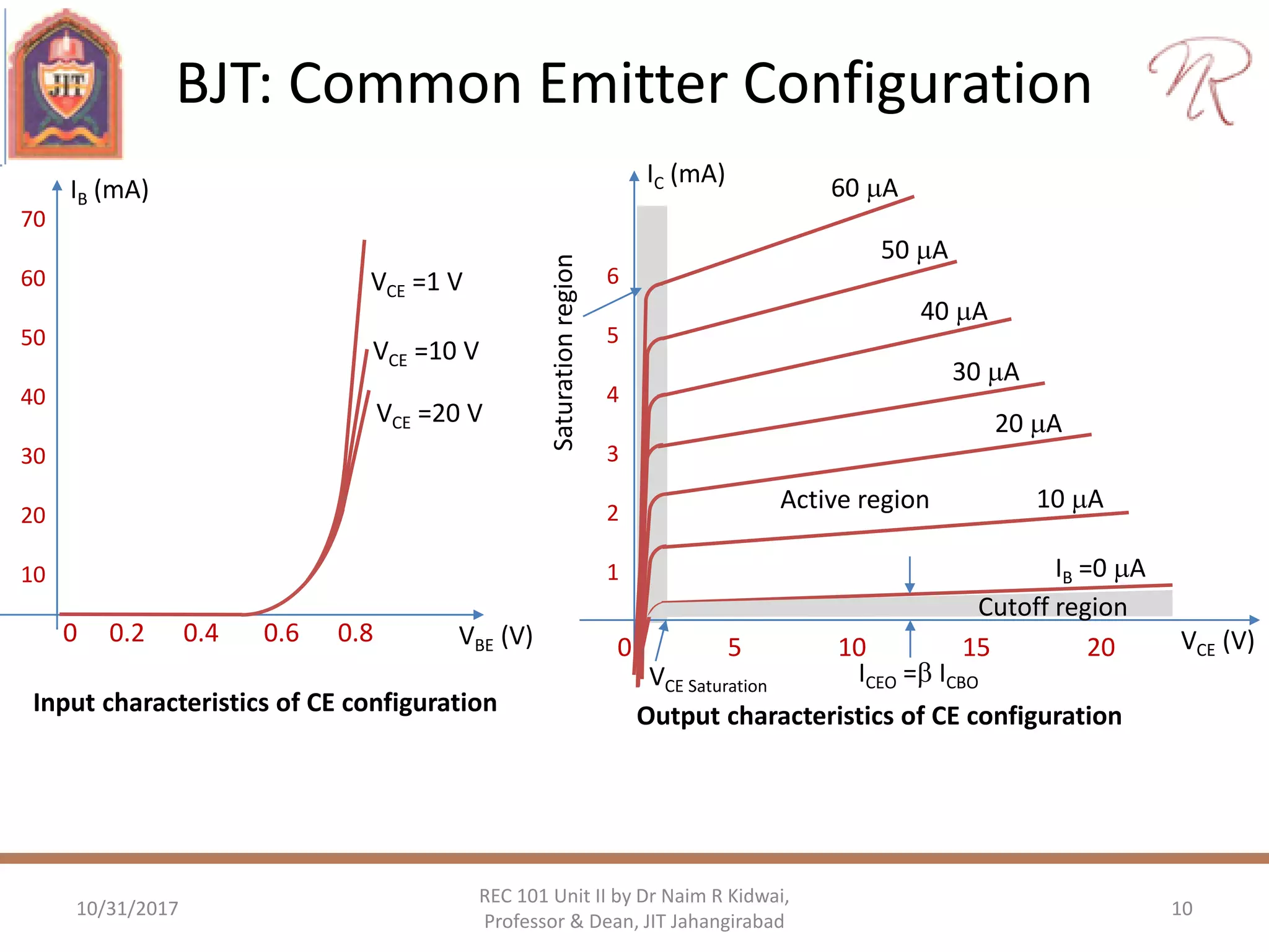
Bipolar Junction Transistor (BJT)
Characteristics
Unit II
Bipolar Junction Transistor: Transistor Construction, Operation, Amplification action.
Common Base, Common Emitter, Common Collector Configuration DC Biasing BJTs:
Operating Point, Fixed-Bias, Emitter Bias, Voltage-Divider Bias Configuration. Collector
Feedback, Emitter-Follower Configuration. Bias Stabilization. CE, CB, CC amplifiers and AC
analysis of single stage CE amplifier (re Model ). Field Effect Transistor: Construction and
Characteristic of JFETs. AC analysis of CS amplifier, MOSFET (Depletion and
Enhancement)Type, Transfer Characteristic
10/31/2017 1
REC 101 Unit II by Dr Naim R Kidwai,
Professor & Dean, JIT Jahangirabad
Bipolar Junction Transistor (BJT): Construction
• Transistor is 3-layer semiconductor device consisting of either n-p-n
layers (npn transistor) or p-n-p layers (pnp transistor).
10/31/2017 2
REC 101 Unit II by Dr Naim R Kidwai,
Professor & Dean, JIT Jahangirabad
Q
E
Emitter
Collector
C
Base B
Q
E
Emitter
Collector
C
Base B
n np
E C
B
p pn
E C
B
npn transistor pnp transistor
Substrate
Collector
base
Emitter
Metal Contact
Oxide layer
Basic epitaxial planar structure
Bipolar Junction Transistor (BJT): Construction
• The arrow in the symbol defines the direction of emitter current.
• The emitter layer is heavily doped in comparison to collector.
• The outer layers have widths much greater than the sandwiched p-
or n -type material. (typically 150:1)
• Doping of sandwiched layer is considerably less than outer layers
(typically, 1:10 or less) resulting in low conductance (high resistance)
• The transistor is called bipolar junction transistor (BJT).Term bipolar
reflects the fact that both polarity of charges (holes and electrons)
participate in current flow.
10/31/2017 3
REC 101 Unit II by Dr Naim R Kidwai,
Professor & Dean, JIT Jahangirabad
BJT: Operation
10/31/2017 4
REC 101 Unit II by Dr Naim R Kidwai,
Professor & Dean, JIT Jahangirabad
• EB junction is forward biased and CB
junction is reverse biased
• Large number of majority carriers
diffuse across forward biased p-n
junction into n material.
• In thin base with low conductivity, few carrier go to base terminal
while most carriers diffuse across reverse biased junction. IB is
typically in microamperes, while IC & IE are in milliamperes.
• Using KCL IE= IC + IB
• IC is mainly due to majority carriers. minority carriers (leakage
current: IC with emitter terminal open) also contribute in IC
IC = IC majority + ICO minority
E C
B
p n p
Majority current
component
Minority current
component
VEE VCC
Depletion layer
IE IC
IB
BJT: Common Base configuration
• Behaviour of BJT is described by two sets of characteristics; driving
point or input parameters and output parameters.
• The input set for the CB amplifier relates an input current (IE) to an
input voltage (VBE) for various levels of output voltage (VCB).
• The output set for the CB amplifier relates an output current (IC) to
an output voltage (VCB) for various levels of input current (IE).
10/31/2017 5
REC 101 Unit II by Dr Naim R Kidwai,
Professor & Dean, JIT Jahangirabad
E C
B
VEE
VCC
IE IC
IB
Q
VBE VCB
E C
B
VEE VCC
IE IC
IB
Q
VBE VCB
Common base configuration pnp transistor Common base configuration npn transistor
BJT: Common Base configuration
10/31/2017 6
REC 101 Unit II by Dr Naim R Kidwai,
Professor & Dean, JIT Jahangirabad
VCB (V)
IE =0 mA
IE =1 mA
2 mA
3 mA
4 mA
5 mA
IC (mA)
6 mA
Cutoff region
Saturationregion
Active region
ICO = ICBO BVCBO
0 10 20 30 40
6
5
4
3
2
1
0
Output characteristics of CB configuration
VBE (V)
VCB =1 V
IE (mA)
0 0.2 0.4 0.6 0.8
7
6
5
4
3
2
1
VCB =10 V
VCB =20 V
Input characteristics of CB configuration
BJT: Common Base configuration
10/31/2017 7
REC 101 Unit II by Dr Naim R Kidwai,
Professor & Dean, JIT Jahangirabad
Input characteristics:
• For a VCB, input characteristic is like diode. If transistor ON, VBE0.7 V
output characteristics: has 3 regions : active, cut-off, and saturation
Active region: normally employed for amplification
• EB junction is forward-biased, & CB junction is reverse-biased.
• For IE=0, collector current IC =ICO=ICBO while for higher IE, IC IE
Cut-off region
• EB junction & CB junction both reverse-biased & no Collector current
Saturation region
• EB junction & CB junction both is forward biased
• IC increases exponentially as the voltage VCB increases toward 0 V
BJT: Common Base configuration
Alpha ()
• Where IC and IE are the currents at the point of operation
• for practical devices alpha typically extends from 0.90 to 0.998
• Since alpha is defined solely for the majority carriers
IC =  IE + ICBO
• Where ICBO is very small and can be ignored in some approximations
Breakdown voltage
• In active region VCB increases beyond a point, due to avalanche
effect, IC rises suddenly.
• The largest permissible VCB before breakdown is labelled as VCBO
10/31/2017 8
REC 101 Unit II by Dr Naim R Kidwai,
Professor & Dean, JIT Jahangirabad
E
C
I
I
gaincurrentbasecommon
BJT: Common Emitter Configuration
• The input set for the CE amplifier relates an input current (IB) to an
input voltage (VBE) for various levels of output voltage (VCE).
• The output set for the CE amplifier relates an output current (IC) to
an output voltage (VCE) for various levels of input current (IB).
10/31/2017 9
REC 101 Unit II by Dr Naim R Kidwai,
Professor & Dean, JIT Jahangirabad
E
C
B
VBB
VCC
IE
IC
IB
Q
VBE
VCE
E
C
B
VBB
VCC
IE
IC
IB
Q
VBE
VCE
Common emitter configuration pnp transistor Common emitter configuration npn transistor
BJT: Common Emitter Configuration
10/31/2017 10
REC 101 Unit II by Dr Naim R Kidwai,
Professor & Dean, JIT Jahangirabad
Output characteristics of CE configuration
VBE (V)
VCE =20 V
IB (mA)
0 0.2 0.4 0.6 0.8
70
60
50
40
30
20
10
VCE =10 V
VCE =1 V
Input characteristics of CE configuration
VCE (V)
IB =0 A
10 A
20 A
40 A
50 A
IC (mA)
60 A
Saturationregion
Active region
ICEO = ICBOVCE Saturation
0 5 10 15 20
6
5
4
3
2
1
30 A
Cutoff region
BJT: Common Emitter Configuration
10/31/2017 11
REC 101 Unit II by Dr Naim R Kidwai,
Professor & Dean, JIT Jahangirabad
Input characteristics:
• For a VCE, input characteristic is like diode. If transistor ON, VBE0.7 V
output characteristics: has 3 regions : active, cut-off, and saturation
Active region: normally employed for amplification
• BE junction is forward-biased, & CB junction is reverse-biased.
• exists to the right of the vertical line at VCE saturation and above the
curve for IB =0. For IB=0, collector current IC =ICEO=ICBO /(1-)
• IC curves are not as horizontal as in CB configuration, VCE affects IC .
Cut-off region: Region below the curve for IB=0,
Saturation region: region to the left of VCE saturation
• IC increases exponentially as VCB increases toward VCE saturation
BJT: Common Emitter Configuration
Beta ()
• Where IC and IB are the currents at the point of operation
• for practical devices Beta typically ranges in between 50 to 400
Relation between Alpha and Beta
10/31/2017 12
REC 101 Unit II by Dr Naim R Kidwai,
Professor & Dean, JIT Jahangirabad
B
C
I
I
gaincurrentemitterCommon


 C
C
C
BCE
I
I
I
III





1 




1
large]veryis[as)1(
1


CBOCBO
CBO
CEO II
I
I 


BJT: Common Collector Configuration
• CC configuration is also known as emitter follower configuration as
the emitter voltage follows the base voltage.
• This configuration is mostly used as a buffer.
• CC configuration is used mainly for impedance-matching, as it has
high-input & low-output impedance, opposite to CB/CE Configuration
10/31/2017 13
REC 101 Unit II by Dr Naim R Kidwai,
Professor & Dean, JIT Jahangirabad
C
E
B
VBB
VEE
IC
IE
IB
Q
VBE
VCE
C
E
B
VBB
VEE
IC
IE
IB
Q
VBE
VCE
Common emitter configuration pnp transistor Common emitter configuration npn transistor
BJT: Common collector Configuration
10/31/2017 14
REC 101 Unit II by Dr Naim R Kidwai,
Professor & Dean, JIT Jahangirabad
Input characteristics of CC configuration
VCB (V)
VEC =2 V
IB (mA)
0 1 2 3 4 5 6
70
60
50
40
30
20
10
VEC =4 V
Output characteristics of CC configuration
VEC (V)
IB =0 A
10 A
20 A
40 A
50 A
IE (mA)
Saturationregion
Active region
0 5 10 15 20
5
4
3
2
1
30 A
Cutoff region
• Input characteristics of the CC configuration is different as current IB
decreases with increase in base collector voltage
• Output characteristics of the CC configuration are the same as of CE
configuration.
BJT: Amplification
• BJT can be used in two modes
– As a switch (operates in cut-off / saturation region of characteristics)
– As an amplifier (operates in active region of characteristics)
• BJT can be employed as an amplifying device in active region (BE
Junction forward biased and CB junction reverse biased).
• In amplification output ac signal power is greater than the input ac
signal power
• Increased ac power is contributed by dc power of transistor biasing
• Amplification factor is ratio of output to input parameter
10/31/2017 15
REC 101 Unit II by Dr Naim R Kidwai,
Professor & Dean, JIT Jahangirabad
i
O
V
V
V
A gainVoltage
i
O
i
I
I
A gainCurrent
ii
OO
i
O
P
IV
IV
P
P
A gainPower

Rec101 unit ii (part 1) bjt characteristics

  • 1.
    Bipolar Junction Transistor(BJT) Characteristics Unit II Bipolar Junction Transistor: Transistor Construction, Operation, Amplification action. Common Base, Common Emitter, Common Collector Configuration DC Biasing BJTs: Operating Point, Fixed-Bias, Emitter Bias, Voltage-Divider Bias Configuration. Collector Feedback, Emitter-Follower Configuration. Bias Stabilization. CE, CB, CC amplifiers and AC analysis of single stage CE amplifier (re Model ). Field Effect Transistor: Construction and Characteristic of JFETs. AC analysis of CS amplifier, MOSFET (Depletion and Enhancement)Type, Transfer Characteristic 10/31/2017 1 REC 101 Unit II by Dr Naim R Kidwai, Professor & Dean, JIT Jahangirabad
  • 2.
    Bipolar Junction Transistor(BJT): Construction • Transistor is 3-layer semiconductor device consisting of either n-p-n layers (npn transistor) or p-n-p layers (pnp transistor). 10/31/2017 2 REC 101 Unit II by Dr Naim R Kidwai, Professor & Dean, JIT Jahangirabad Q E Emitter Collector C Base B Q E Emitter Collector C Base B n np E C B p pn E C B npn transistor pnp transistor Substrate Collector base Emitter Metal Contact Oxide layer Basic epitaxial planar structure
  • 3.
    Bipolar Junction Transistor(BJT): Construction • The arrow in the symbol defines the direction of emitter current. • The emitter layer is heavily doped in comparison to collector. • The outer layers have widths much greater than the sandwiched p- or n -type material. (typically 150:1) • Doping of sandwiched layer is considerably less than outer layers (typically, 1:10 or less) resulting in low conductance (high resistance) • The transistor is called bipolar junction transistor (BJT).Term bipolar reflects the fact that both polarity of charges (holes and electrons) participate in current flow. 10/31/2017 3 REC 101 Unit II by Dr Naim R Kidwai, Professor & Dean, JIT Jahangirabad
  • 4.
    BJT: Operation 10/31/2017 4 REC101 Unit II by Dr Naim R Kidwai, Professor & Dean, JIT Jahangirabad • EB junction is forward biased and CB junction is reverse biased • Large number of majority carriers diffuse across forward biased p-n junction into n material. • In thin base with low conductivity, few carrier go to base terminal while most carriers diffuse across reverse biased junction. IB is typically in microamperes, while IC & IE are in milliamperes. • Using KCL IE= IC + IB • IC is mainly due to majority carriers. minority carriers (leakage current: IC with emitter terminal open) also contribute in IC IC = IC majority + ICO minority E C B p n p Majority current component Minority current component VEE VCC Depletion layer IE IC IB
  • 5.
    BJT: Common Baseconfiguration • Behaviour of BJT is described by two sets of characteristics; driving point or input parameters and output parameters. • The input set for the CB amplifier relates an input current (IE) to an input voltage (VBE) for various levels of output voltage (VCB). • The output set for the CB amplifier relates an output current (IC) to an output voltage (VCB) for various levels of input current (IE). 10/31/2017 5 REC 101 Unit II by Dr Naim R Kidwai, Professor & Dean, JIT Jahangirabad E C B VEE VCC IE IC IB Q VBE VCB E C B VEE VCC IE IC IB Q VBE VCB Common base configuration pnp transistor Common base configuration npn transistor
  • 6.
    BJT: Common Baseconfiguration 10/31/2017 6 REC 101 Unit II by Dr Naim R Kidwai, Professor & Dean, JIT Jahangirabad VCB (V) IE =0 mA IE =1 mA 2 mA 3 mA 4 mA 5 mA IC (mA) 6 mA Cutoff region Saturationregion Active region ICO = ICBO BVCBO 0 10 20 30 40 6 5 4 3 2 1 0 Output characteristics of CB configuration VBE (V) VCB =1 V IE (mA) 0 0.2 0.4 0.6 0.8 7 6 5 4 3 2 1 VCB =10 V VCB =20 V Input characteristics of CB configuration
  • 7.
    BJT: Common Baseconfiguration 10/31/2017 7 REC 101 Unit II by Dr Naim R Kidwai, Professor & Dean, JIT Jahangirabad Input characteristics: • For a VCB, input characteristic is like diode. If transistor ON, VBE0.7 V output characteristics: has 3 regions : active, cut-off, and saturation Active region: normally employed for amplification • EB junction is forward-biased, & CB junction is reverse-biased. • For IE=0, collector current IC =ICO=ICBO while for higher IE, IC IE Cut-off region • EB junction & CB junction both reverse-biased & no Collector current Saturation region • EB junction & CB junction both is forward biased • IC increases exponentially as the voltage VCB increases toward 0 V
  • 8.
    BJT: Common Baseconfiguration Alpha () • Where IC and IE are the currents at the point of operation • for practical devices alpha typically extends from 0.90 to 0.998 • Since alpha is defined solely for the majority carriers IC =  IE + ICBO • Where ICBO is very small and can be ignored in some approximations Breakdown voltage • In active region VCB increases beyond a point, due to avalanche effect, IC rises suddenly. • The largest permissible VCB before breakdown is labelled as VCBO 10/31/2017 8 REC 101 Unit II by Dr Naim R Kidwai, Professor & Dean, JIT Jahangirabad E C I I gaincurrentbasecommon
  • 9.
    BJT: Common EmitterConfiguration • The input set for the CE amplifier relates an input current (IB) to an input voltage (VBE) for various levels of output voltage (VCE). • The output set for the CE amplifier relates an output current (IC) to an output voltage (VCE) for various levels of input current (IB). 10/31/2017 9 REC 101 Unit II by Dr Naim R Kidwai, Professor & Dean, JIT Jahangirabad E C B VBB VCC IE IC IB Q VBE VCE E C B VBB VCC IE IC IB Q VBE VCE Common emitter configuration pnp transistor Common emitter configuration npn transistor
  • 10.
    BJT: Common EmitterConfiguration 10/31/2017 10 REC 101 Unit II by Dr Naim R Kidwai, Professor & Dean, JIT Jahangirabad Output characteristics of CE configuration VBE (V) VCE =20 V IB (mA) 0 0.2 0.4 0.6 0.8 70 60 50 40 30 20 10 VCE =10 V VCE =1 V Input characteristics of CE configuration VCE (V) IB =0 A 10 A 20 A 40 A 50 A IC (mA) 60 A Saturationregion Active region ICEO = ICBOVCE Saturation 0 5 10 15 20 6 5 4 3 2 1 30 A Cutoff region
  • 11.
    BJT: Common EmitterConfiguration 10/31/2017 11 REC 101 Unit II by Dr Naim R Kidwai, Professor & Dean, JIT Jahangirabad Input characteristics: • For a VCE, input characteristic is like diode. If transistor ON, VBE0.7 V output characteristics: has 3 regions : active, cut-off, and saturation Active region: normally employed for amplification • BE junction is forward-biased, & CB junction is reverse-biased. • exists to the right of the vertical line at VCE saturation and above the curve for IB =0. For IB=0, collector current IC =ICEO=ICBO /(1-) • IC curves are not as horizontal as in CB configuration, VCE affects IC . Cut-off region: Region below the curve for IB=0, Saturation region: region to the left of VCE saturation • IC increases exponentially as VCB increases toward VCE saturation
  • 12.
    BJT: Common EmitterConfiguration Beta () • Where IC and IB are the currents at the point of operation • for practical devices Beta typically ranges in between 50 to 400 Relation between Alpha and Beta 10/31/2017 12 REC 101 Unit II by Dr Naim R Kidwai, Professor & Dean, JIT Jahangirabad B C I I gaincurrentemitterCommon    C C C BCE I I I III      1      1 large]veryis[as)1( 1   CBOCBO CBO CEO II I I   
  • 13.
    BJT: Common CollectorConfiguration • CC configuration is also known as emitter follower configuration as the emitter voltage follows the base voltage. • This configuration is mostly used as a buffer. • CC configuration is used mainly for impedance-matching, as it has high-input & low-output impedance, opposite to CB/CE Configuration 10/31/2017 13 REC 101 Unit II by Dr Naim R Kidwai, Professor & Dean, JIT Jahangirabad C E B VBB VEE IC IE IB Q VBE VCE C E B VBB VEE IC IE IB Q VBE VCE Common emitter configuration pnp transistor Common emitter configuration npn transistor
  • 14.
    BJT: Common collectorConfiguration 10/31/2017 14 REC 101 Unit II by Dr Naim R Kidwai, Professor & Dean, JIT Jahangirabad Input characteristics of CC configuration VCB (V) VEC =2 V IB (mA) 0 1 2 3 4 5 6 70 60 50 40 30 20 10 VEC =4 V Output characteristics of CC configuration VEC (V) IB =0 A 10 A 20 A 40 A 50 A IE (mA) Saturationregion Active region 0 5 10 15 20 5 4 3 2 1 30 A Cutoff region • Input characteristics of the CC configuration is different as current IB decreases with increase in base collector voltage • Output characteristics of the CC configuration are the same as of CE configuration.
  • 15.
    BJT: Amplification • BJTcan be used in two modes – As a switch (operates in cut-off / saturation region of characteristics) – As an amplifier (operates in active region of characteristics) • BJT can be employed as an amplifying device in active region (BE Junction forward biased and CB junction reverse biased). • In amplification output ac signal power is greater than the input ac signal power • Increased ac power is contributed by dc power of transistor biasing • Amplification factor is ratio of output to input parameter 10/31/2017 15 REC 101 Unit II by Dr Naim R Kidwai, Professor & Dean, JIT Jahangirabad i O V V V A gainVoltage i O i I I A gainCurrent ii OO i O P IV IV P P A gainPower