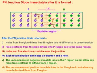
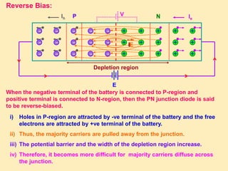
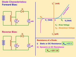
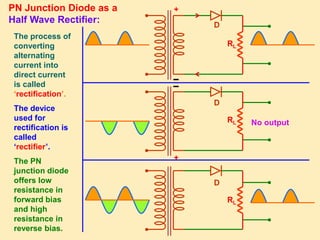
SlideShare a Scribd company logo
1 of 12
SOLIDS AND SEMICONDUCTOR DEVICES - II
1. PN Junction Diode
2. Forward Bias of Junction Diode
3. Reverse Bias of Junction Diode
4. Diode Characteristics
5. Static and Dynamic Resistance of a Diode
6. Diode as a Half Wave Rectifier
7. Diode as a Full Wave Rectifier
Created by C. Mani, Principal, K V No.1, AFS, Jalahalli West, Bangalore
PN Junction Diode:
+
-
Mobile Hole (Majority Carrier)
Immobile Negative Impurity Ion
Mobile Electron (Majority Carrier)
Immobile Positive Impurity Ion
+
+
+
+
+
+
+
+
+
-
-
-
-
-
-
-
-
-
P N
-
-
-
-
-
-
+
+
+
+
+
+
When a P-type semiconductor is joined to a N-type semiconductor such
that the crystal structure remains continuous at the boundary, the resulting
arrangement is called a PN junction diode or a semiconductor diode or a
crystal diode.
When a PN junction is formed, the
P region has mobile holes (+) and
immobile negatively charged ions.
N region has mobile electrons (-) and
immobile positively charged ions.
The whole arrangement is electrically neutral.
For simplicity, the minority charge carriers are not shown in the figure.
+
+
+
-
-
-
P N
-
-
-
-
-
-
+
+
+
+
+
+
-
-
-
-
-
-
+
+
+
+
+
+
PN Junction Diode immediately after it is formed :
After the PN junction diode is formed –
i) Holes from P region diffuse into N region due to difference in concentration.
ii) Free electrons from N region diffuse into P region due to the same reason.
iii) Holes and free electrons combine near the junction.
iv) Each recombination eliminates an electron and a hole.
v) The uncompensated negative immobile ions in the P region do not allow any
more free electrons to diffuse from N region.
vi) The uncompensated positive immobile ions in the N region do not allow any
more holes to diffuse from P region.
Fr
Fr
E
V
Depletion region
vii) The positive donor ions in the N region and the negative acceptor ions in
the P region are left uncompensated.
viii) The region containing the uncompensated acceptor and donor ions is
called ‘depletion region’ because this region is devoid of mobile charges.
Since the region is having only immobile charges, therefore, this region
is also called ‘space charge region’.
ix) The N region is having higher potential than P region.
x) So, an electric field is set up as shown in the figure.
xi) The difference in potential between P and N regions across the junction
makes it difficult for the holes and electrons to move across the junction.
This acts as a barrier and hence called ‘potential barrier’ or ‘height of the
barrier’.
xii) The physical distance between one side and the other side of the barrier is
called ‘width of the barrier’.
xiii) Potential barrier for Si is nearly 0.7 V and for Ge is 0.3 V.
xiv) The potential barrier opposes the motion of the majority carriers.
xv) However, a few majority carriers with high kinetic energy manage to
overcome the barrier and cross the junction.
ix) Potential barrier helps the movement of minority carriers.
Forward Bias:
When the positive terminal of the battery is connected to P-region and
negative terminal is connected to N-region, then the PN junction diode is said
to be forward-biased.
+
+
+
+
+
+
-
-
-
-
-
-
P N
-
-
-
-
-
-
+
+
+
+
+
+
+
+
+
-
-
-
E
Depletion region
E
Ie
Ih
i) Holes in P-region are repelled by +ve terminal of the battery and the free
electrons are repelled by –ve terminal of the battery.
ii) So, some holes and free electrons enter into the depletion region.
iii) The potential barrier and the width of the depletion region decrease.
iv) Therefore, a large number of majority carriers diffuse across the junction.
v) Hole current and electronic current are in the same direction and add up.
+
+
+
-
-
-
P N
-
-
-
-
-
-
+
+
+
+
+
+
-
-
-
-
-
-
+
+
+
+
+
+
E
V
v) Once they cross the junction, the holes in N-region and the electrons in P-
region become minority carriers of charge and constitute minority
current.
vi) For each electron – hole recombination, an electron from the negative
terminal of the battery enters the N-region and then drifts towards the
junction.
In the P-region, near the positive terminal of the battery, an electron
breaks covalent bond in the crystal and thus a hole is created. The hole
drifts towards the junction and the electron enters the positive terminal of
the battery.
vii) Thus, the current in the external circuit is due to movement of electrons,
current in P-region is due to movement of holes and current in N-region is
due to movement of electrons.
viii) If the applied potential is increased, the potential barrier further
decreases. As a result, a large number of majority carriers diffuse
through the junction and a larger current flows.
When the negative terminal of the battery is connected to P-region and
positive terminal is connected to N-region, then the PN junction diode is said
to be reverse-biased.
i) Holes in P-region are attracted by -ve terminal of the battery and the free
electrons are attracted by +ve terminal of the battery.
ii) Thus, the majority carriers are pulled away from the junction.
iii) The potential barrier and the width of the depletion region increase.
iv) Therefore, it becomes more difficult for majority carriers diffuse across
the junction.
Reverse Bias:
V
+
+
+
+
+
+
-
-
-
-
-
-
P N
-
-
-
-
-
-
+
+
+
+
+
+
+
+
+
-
-
-
E
Depletion region
E
Ie
Ih
+
+
+
-
-
-
P N
-
-
-
-
-
-
+
+
+
+
+
+
-
-
-
-
-
-
+
+
+
+
+
+
E
V
v) But the potential barrier helps the movement of the minority carriers. As
soon as the minority carriers are generated, they are swept away by the
potential barrier.
vi) At a given temperature, the rate of generation of minority carriers is
constant.
vii) So, the resulting current is constant irrespective of the applied voltage.
For this reason, this current is called ‘reverse saturation current’.
viii) Since the number of minority carriers is small, therefore, this current is
small and is in the order of 10-9 A in silicon diode and 10-6 A in germanium
diode.
ix) The reverse – biased PN junction diode has an effective capacitance
called ‘transition or depletion capacitance’. P and N regions act as the
plates of the capacitor and the depletion region acts as a dielectric
medium.
Vf (Volt)
If (mA)
Ir (μA)
Vr (Volt) Vk
VB
Diode Characteristics:
mA
+
V
+
Forward Bias:
Reverse Bias:
D
μA
+
V
+
D
Resistance of a Diode:
i) Static or DC Resistance Rd.c = V / I
ii) Dynamic or AC Resistance
Ra.c = ΔV / ΔI
Vk – Knee Voltage
VB – Breakdown Voltage
0
PN Junction Diode as a
Half Wave Rectifier: D
RL
●
●
●
●
+
D
RL
●
●
●
●
+
No output
D
RL
●
●
●
●
The process of
converting
alternating
current into
direct current
is called
‘rectification’.
The device
used for
rectification is
called
‘rectifier’.
The PN
junction diode
offers low
resistance in
forward bias
and high
resistance in
reverse bias.
D1
RL
●
●
+
PN Junction Diode as a
Full Wave Rectifier:
D2
●
●
A B
+
RL
●
●
●
●
A B
D1
D2
RL
●
●
●
●
A B
D1
D2
When the diode
rectifies whole
of the AC wave,
it is called ‘full
wave rectifier’.
During the
positive half
cycle of the
input ac signal,
the diode D1
conducts and
current is
through BA.
During the
negative half
cycle, the diode
D2 conducts
and current is
through BA.
Special Purpose p-n Junction Diodes:
Zener Diode
Vf (Volt)
If (mA)
Ir (μA)
Vr (Volt)
VZ
Vz – Breakdown Voltage
0
Zener Diode as a Voltage Regulator
RL
●
RS
●
●
●
Unregulated
Voltage
V
L
Regulated
Voltage VZ
• Heavily doped
• Depletion Region is < 10-6 m
• Electric Field is very high (5x10⁶ V/m)
•Reverse biased
•Internal Field emission or field
ionisation
End of S & SC - II

More Related Content

Similar to solids_and_semiconductor_devices_2.ppt

Semiconductor diodes1
Semiconductor diodes1Semiconductor diodes1
Semiconductor diodes1Sirat Mahmood
 
Electronics Engineering Diode , Transistor ,BJT
Electronics Engineering Diode , Transistor ,BJTElectronics Engineering Diode , Transistor ,BJT
Electronics Engineering Diode , Transistor ,BJTyadavsuyash008
 
01 pn junction diode characteristics prp
01 pn junction diode characteristics prp01 pn junction diode characteristics prp
01 pn junction diode characteristics prpDr. Pravin Prajapati
 
EC8252-Electronic Devices Question Bank.pdf
EC8252-Electronic Devices Question Bank.pdfEC8252-Electronic Devices Question Bank.pdf
EC8252-Electronic Devices Question Bank.pdfRajaSekaran923497
 
Introduction to Semiconductor Materials and devices
Introduction to Semiconductor Materials and devicesIntroduction to Semiconductor Materials and devices
Introduction to Semiconductor Materials and devicesArunbhaarat S
 
Electronics ichapter1
Electronics ichapter1Electronics ichapter1
Electronics ichapter1Ankit Dubey
 
Class 12 th semiconductor part 3
Class 12 th semiconductor part 3Class 12 th semiconductor part 3
Class 12 th semiconductor part 3Priyanka Jakhar
 
Analog circuits-lab-possible-viva-questions
Analog circuits-lab-possible-viva-questionsAnalog circuits-lab-possible-viva-questions
Analog circuits-lab-possible-viva-questionspadmajasiva
 
diodecurren-jntu.pdf
diodecurren-jntu.pdfdiodecurren-jntu.pdf
diodecurren-jntu.pdfjayand4
 
Minor project report on pn junction, zener diode, led characteristics
Minor project report on pn junction, zener diode, led characteristicsMinor project report on pn junction, zener diode, led characteristics
Minor project report on pn junction, zener diode, led characteristicsom prakash bishnoi
 
Pn junction diode class 12 investegatory project
Pn junction diode class 12 investegatory projectPn junction diode class 12 investegatory project
Pn junction diode class 12 investegatory projectabhijeet singh
 
227 sample chapter
227 sample chapter227 sample chapter
227 sample chapterAnkit Dubey
 
Basics of p-n Junction Diode.pdf
Basics of p-n Junction Diode.pdfBasics of p-n Junction Diode.pdf
Basics of p-n Junction Diode.pdfDr Biplab Bag
 

Similar to solids_and_semiconductor_devices_2.ppt (20)

Semiconductor diodes1
Semiconductor diodes1Semiconductor diodes1
Semiconductor diodes1
 
Theory of solids
Theory of solidsTheory of solids
Theory of solids
 
Electronics Engineering Diode , Transistor ,BJT
Electronics Engineering Diode , Transistor ,BJTElectronics Engineering Diode , Transistor ,BJT
Electronics Engineering Diode , Transistor ,BJT
 
01 pn junction diode characteristics prp
01 pn junction diode characteristics prp01 pn junction diode characteristics prp
01 pn junction diode characteristics prp
 
EC8252-Electronic Devices Question Bank.pdf
EC8252-Electronic Devices Question Bank.pdfEC8252-Electronic Devices Question Bank.pdf
EC8252-Electronic Devices Question Bank.pdf
 
BEEE.pptx
BEEE.pptxBEEE.pptx
BEEE.pptx
 
Introduction to Semiconductor Materials and devices
Introduction to Semiconductor Materials and devicesIntroduction to Semiconductor Materials and devices
Introduction to Semiconductor Materials and devices
 
Electronics ichapter1
Electronics ichapter1Electronics ichapter1
Electronics ichapter1
 
Vivalab
VivalabVivalab
Vivalab
 
Class 12 th semiconductor part 3
Class 12 th semiconductor part 3Class 12 th semiconductor part 3
Class 12 th semiconductor part 3
 
Analog circuits-lab-possible-viva-questions
Analog circuits-lab-possible-viva-questionsAnalog circuits-lab-possible-viva-questions
Analog circuits-lab-possible-viva-questions
 
AE UNIT I.ppt
AE UNIT I.pptAE UNIT I.ppt
AE UNIT I.ppt
 
diodecurren-jntu.pdf
diodecurren-jntu.pdfdiodecurren-jntu.pdf
diodecurren-jntu.pdf
 
tunnel.ppt
tunnel.ppttunnel.ppt
tunnel.ppt
 
EC 8353 EDC
EC 8353 EDCEC 8353 EDC
EC 8353 EDC
 
Minor project report on pn junction, zener diode, led characteristics
Minor project report on pn junction, zener diode, led characteristicsMinor project report on pn junction, zener diode, led characteristics
Minor project report on pn junction, zener diode, led characteristics
 
Pn junction diode class 12 investegatory project
Pn junction diode class 12 investegatory projectPn junction diode class 12 investegatory project
Pn junction diode class 12 investegatory project
 
Semiconductors
SemiconductorsSemiconductors
Semiconductors
 
227 sample chapter
227 sample chapter227 sample chapter
227 sample chapter
 
Basics of p-n Junction Diode.pdf
Basics of p-n Junction Diode.pdfBasics of p-n Junction Diode.pdf
Basics of p-n Junction Diode.pdf
 

More from jnvldh2000

current electricity physics Add more information to your upload
current electricity physics Add more information to your uploadcurrent electricity physics Add more information to your upload
current electricity physics Add more information to your uploadjnvldh2000
 
payoffoptions2-191030161254.pptx
payoffoptions2-191030161254.pptxpayoffoptions2-191030161254.pptx
payoffoptions2-191030161254.pptxjnvldh2000
 
Theory_of_Production
Theory_of_ProductionTheory_of_Production
Theory_of_Productionjnvldh2000
 
3_Wave_Optics_1.pptx
3_Wave_Optics_1.pptx3_Wave_Optics_1.pptx
3_Wave_Optics_1.pptxjnvldh2000
 
Revised marking scheme of class 12 maths.pdf
Revised marking scheme of class 12 maths.pdfRevised marking scheme of class 12 maths.pdf
Revised marking scheme of class 12 maths.pdfjnvldh2000
 
ANURAG CS Project.docx
ANURAG CS Project.docxANURAG CS Project.docx
ANURAG CS Project.docxjnvldh2000
 
Anmol chem project.docx
Anmol chem project.docxAnmol chem project.docx
Anmol chem project.docxjnvldh2000
 

More from jnvldh2000 (8)

current electricity physics Add more information to your upload
current electricity physics Add more information to your uploadcurrent electricity physics Add more information to your upload
current electricity physics Add more information to your upload
 
payoffoptions2-191030161254.pptx
payoffoptions2-191030161254.pptxpayoffoptions2-191030161254.pptx
payoffoptions2-191030161254.pptx
 
Theory_of_Production
Theory_of_ProductionTheory_of_Production
Theory_of_Production
 
economics
economicseconomics
economics
 
3_Wave_Optics_1.pptx
3_Wave_Optics_1.pptx3_Wave_Optics_1.pptx
3_Wave_Optics_1.pptx
 
Revised marking scheme of class 12 maths.pdf
Revised marking scheme of class 12 maths.pdfRevised marking scheme of class 12 maths.pdf
Revised marking scheme of class 12 maths.pdf
 
ANURAG CS Project.docx
ANURAG CS Project.docxANURAG CS Project.docx
ANURAG CS Project.docx
 
Anmol chem project.docx
Anmol chem project.docxAnmol chem project.docx
Anmol chem project.docx
 

Recently uploaded

Graduate Outcomes Presentation Slides - English (v3).pptx
Graduate Outcomes Presentation Slides - English (v3).pptxGraduate Outcomes Presentation Slides - English (v3).pptx
Graduate Outcomes Presentation Slides - English (v3).pptxneillewis46
 
Trauma-Informed Leadership - Five Practical Principles
Trauma-Informed Leadership - Five Practical PrinciplesTrauma-Informed Leadership - Five Practical Principles
Trauma-Informed Leadership - Five Practical PrinciplesPooky Knightsmith
 
ANTI PARKISON DRUGS.pptx
ANTI         PARKISON          DRUGS.pptxANTI         PARKISON          DRUGS.pptx
ANTI PARKISON DRUGS.pptxPoojaSen20
 
How To Create Editable Tree View in Odoo 17
How To Create Editable Tree View in Odoo 17How To Create Editable Tree View in Odoo 17
How To Create Editable Tree View in Odoo 17Celine George
 
Transparency, Recognition and the role of eSealing - Ildiko Mazar and Koen No...
Transparency, Recognition and the role of eSealing - Ildiko Mazar and Koen No...Transparency, Recognition and the role of eSealing - Ildiko Mazar and Koen No...
Transparency, Recognition and the role of eSealing - Ildiko Mazar and Koen No...EADTU
 
會考英文會考英文會考英文會考英文會考英文會考英文會考英文會考英文會考英文會考英文會考英文
會考英文會考英文會考英文會考英文會考英文會考英文會考英文會考英文會考英文會考英文會考英文會考英文會考英文會考英文會考英文會考英文會考英文會考英文會考英文會考英文會考英文會考英文
會考英文會考英文會考英文會考英文會考英文會考英文會考英文會考英文會考英文會考英文會考英文中 央社
 
How to Manage Website in Odoo 17 Studio App.pptx
How to Manage Website in Odoo 17 Studio App.pptxHow to Manage Website in Odoo 17 Studio App.pptx
How to Manage Website in Odoo 17 Studio App.pptxCeline George
 
MOOD STABLIZERS DRUGS.pptx
MOOD     STABLIZERS           DRUGS.pptxMOOD     STABLIZERS           DRUGS.pptx
MOOD STABLIZERS DRUGS.pptxPoojaSen20
 
會考英聽會考英聽會考英聽會考英聽會考英聽會考英聽會考英聽會考英聽會考英聽會考英聽
會考英聽會考英聽會考英聽會考英聽會考英聽會考英聽會考英聽會考英聽會考英聽會考英聽會考英聽會考英聽會考英聽會考英聽會考英聽會考英聽會考英聽會考英聽會考英聽會考英聽
會考英聽會考英聽會考英聽會考英聽會考英聽會考英聽會考英聽會考英聽會考英聽會考英聽中 央社
 
Book Review of Run For Your Life Powerpoint
Book Review of Run For Your Life PowerpointBook Review of Run For Your Life Powerpoint
Book Review of Run For Your Life Powerpoint23600690
 
Major project report on Tata Motors and its marketing strategies
Major project report on Tata Motors and its marketing strategiesMajor project report on Tata Motors and its marketing strategies
Major project report on Tata Motors and its marketing strategiesAmanpreetKaur157993
 
Basic Civil Engineering notes on Transportation Engineering & Modes of Transport
Basic Civil Engineering notes on Transportation Engineering & Modes of TransportBasic Civil Engineering notes on Transportation Engineering & Modes of Transport
Basic Civil Engineering notes on Transportation Engineering & Modes of TransportDenish Jangid
 
UChicago CMSC 23320 - The Best Commit Messages of 2024
UChicago CMSC 23320 - The Best Commit Messages of 2024UChicago CMSC 23320 - The Best Commit Messages of 2024
UChicago CMSC 23320 - The Best Commit Messages of 2024Borja Sotomayor
 
24 ĐỀ THAM KHẢO KÌ THI TUYỂN SINH VÀO LỚP 10 MÔN TIẾNG ANH SỞ GIÁO DỤC HẢI DƯ...
24 ĐỀ THAM KHẢO KÌ THI TUYỂN SINH VÀO LỚP 10 MÔN TIẾNG ANH SỞ GIÁO DỤC HẢI DƯ...24 ĐỀ THAM KHẢO KÌ THI TUYỂN SINH VÀO LỚP 10 MÔN TIẾNG ANH SỞ GIÁO DỤC HẢI DƯ...
24 ĐỀ THAM KHẢO KÌ THI TUYỂN SINH VÀO LỚP 10 MÔN TIẾNG ANH SỞ GIÁO DỤC HẢI DƯ...Nguyen Thanh Tu Collection
 
DEMONSTRATION LESSON IN ENGLISH 4 MATATAG CURRICULUM
DEMONSTRATION LESSON IN ENGLISH 4 MATATAG CURRICULUMDEMONSTRATION LESSON IN ENGLISH 4 MATATAG CURRICULUM
DEMONSTRATION LESSON IN ENGLISH 4 MATATAG CURRICULUMELOISARIVERA8
 

Recently uploaded (20)

Graduate Outcomes Presentation Slides - English (v3).pptx
Graduate Outcomes Presentation Slides - English (v3).pptxGraduate Outcomes Presentation Slides - English (v3).pptx
Graduate Outcomes Presentation Slides - English (v3).pptx
 
Trauma-Informed Leadership - Five Practical Principles
Trauma-Informed Leadership - Five Practical PrinciplesTrauma-Informed Leadership - Five Practical Principles
Trauma-Informed Leadership - Five Practical Principles
 
ANTI PARKISON DRUGS.pptx
ANTI         PARKISON          DRUGS.pptxANTI         PARKISON          DRUGS.pptx
ANTI PARKISON DRUGS.pptx
 
How To Create Editable Tree View in Odoo 17
How To Create Editable Tree View in Odoo 17How To Create Editable Tree View in Odoo 17
How To Create Editable Tree View in Odoo 17
 
Transparency, Recognition and the role of eSealing - Ildiko Mazar and Koen No...
Transparency, Recognition and the role of eSealing - Ildiko Mazar and Koen No...Transparency, Recognition and the role of eSealing - Ildiko Mazar and Koen No...
Transparency, Recognition and the role of eSealing - Ildiko Mazar and Koen No...
 
會考英文會考英文會考英文會考英文會考英文會考英文會考英文會考英文會考英文會考英文會考英文
會考英文會考英文會考英文會考英文會考英文會考英文會考英文會考英文會考英文會考英文會考英文會考英文會考英文會考英文會考英文會考英文會考英文會考英文會考英文會考英文會考英文會考英文
會考英文會考英文會考英文會考英文會考英文會考英文會考英文會考英文會考英文會考英文會考英文
 
How to Manage Website in Odoo 17 Studio App.pptx
How to Manage Website in Odoo 17 Studio App.pptxHow to Manage Website in Odoo 17 Studio App.pptx
How to Manage Website in Odoo 17 Studio App.pptx
 
ESSENTIAL of (CS/IT/IS) class 07 (Networks)
ESSENTIAL of (CS/IT/IS) class 07 (Networks)ESSENTIAL of (CS/IT/IS) class 07 (Networks)
ESSENTIAL of (CS/IT/IS) class 07 (Networks)
 
MOOD STABLIZERS DRUGS.pptx
MOOD     STABLIZERS           DRUGS.pptxMOOD     STABLIZERS           DRUGS.pptx
MOOD STABLIZERS DRUGS.pptx
 
會考英聽會考英聽會考英聽會考英聽會考英聽會考英聽會考英聽會考英聽會考英聽會考英聽
會考英聽會考英聽會考英聽會考英聽會考英聽會考英聽會考英聽會考英聽會考英聽會考英聽會考英聽會考英聽會考英聽會考英聽會考英聽會考英聽會考英聽會考英聽會考英聽會考英聽
會考英聽會考英聽會考英聽會考英聽會考英聽會考英聽會考英聽會考英聽會考英聽會考英聽
 
VAMOS CUIDAR DO NOSSO PLANETA! .
VAMOS CUIDAR DO NOSSO PLANETA!                    .VAMOS CUIDAR DO NOSSO PLANETA!                    .
VAMOS CUIDAR DO NOSSO PLANETA! .
 
Book Review of Run For Your Life Powerpoint
Book Review of Run For Your Life PowerpointBook Review of Run For Your Life Powerpoint
Book Review of Run For Your Life Powerpoint
 
Major project report on Tata Motors and its marketing strategies
Major project report on Tata Motors and its marketing strategiesMajor project report on Tata Motors and its marketing strategies
Major project report on Tata Motors and its marketing strategies
 
Mattingly "AI & Prompt Design: Named Entity Recognition"
Mattingly "AI & Prompt Design: Named Entity Recognition"Mattingly "AI & Prompt Design: Named Entity Recognition"
Mattingly "AI & Prompt Design: Named Entity Recognition"
 
Basic Civil Engineering notes on Transportation Engineering & Modes of Transport
Basic Civil Engineering notes on Transportation Engineering & Modes of TransportBasic Civil Engineering notes on Transportation Engineering & Modes of Transport
Basic Civil Engineering notes on Transportation Engineering & Modes of Transport
 
UChicago CMSC 23320 - The Best Commit Messages of 2024
UChicago CMSC 23320 - The Best Commit Messages of 2024UChicago CMSC 23320 - The Best Commit Messages of 2024
UChicago CMSC 23320 - The Best Commit Messages of 2024
 
24 ĐỀ THAM KHẢO KÌ THI TUYỂN SINH VÀO LỚP 10 MÔN TIẾNG ANH SỞ GIÁO DỤC HẢI DƯ...
24 ĐỀ THAM KHẢO KÌ THI TUYỂN SINH VÀO LỚP 10 MÔN TIẾNG ANH SỞ GIÁO DỤC HẢI DƯ...24 ĐỀ THAM KHẢO KÌ THI TUYỂN SINH VÀO LỚP 10 MÔN TIẾNG ANH SỞ GIÁO DỤC HẢI DƯ...
24 ĐỀ THAM KHẢO KÌ THI TUYỂN SINH VÀO LỚP 10 MÔN TIẾNG ANH SỞ GIÁO DỤC HẢI DƯ...
 
Including Mental Health Support in Project Delivery, 14 May.pdf
Including Mental Health Support in Project Delivery, 14 May.pdfIncluding Mental Health Support in Project Delivery, 14 May.pdf
Including Mental Health Support in Project Delivery, 14 May.pdf
 
Supporting Newcomer Multilingual Learners
Supporting Newcomer  Multilingual LearnersSupporting Newcomer  Multilingual Learners
Supporting Newcomer Multilingual Learners
 
DEMONSTRATION LESSON IN ENGLISH 4 MATATAG CURRICULUM
DEMONSTRATION LESSON IN ENGLISH 4 MATATAG CURRICULUMDEMONSTRATION LESSON IN ENGLISH 4 MATATAG CURRICULUM
DEMONSTRATION LESSON IN ENGLISH 4 MATATAG CURRICULUM
 

solids_and_semiconductor_devices_2.ppt

  • 1. SOLIDS AND SEMICONDUCTOR DEVICES - II 1. PN Junction Diode 2. Forward Bias of Junction Diode 3. Reverse Bias of Junction Diode 4. Diode Characteristics 5. Static and Dynamic Resistance of a Diode 6. Diode as a Half Wave Rectifier 7. Diode as a Full Wave Rectifier Created by C. Mani, Principal, K V No.1, AFS, Jalahalli West, Bangalore
  • 2. PN Junction Diode: + - Mobile Hole (Majority Carrier) Immobile Negative Impurity Ion Mobile Electron (Majority Carrier) Immobile Positive Impurity Ion + + + + + + + + + - - - - - - - - - P N - - - - - - + + + + + + When a P-type semiconductor is joined to a N-type semiconductor such that the crystal structure remains continuous at the boundary, the resulting arrangement is called a PN junction diode or a semiconductor diode or a crystal diode. When a PN junction is formed, the P region has mobile holes (+) and immobile negatively charged ions. N region has mobile electrons (-) and immobile positively charged ions. The whole arrangement is electrically neutral. For simplicity, the minority charge carriers are not shown in the figure.
  • 3. + + + - - - P N - - - - - - + + + + + + - - - - - - + + + + + + PN Junction Diode immediately after it is formed : After the PN junction diode is formed – i) Holes from P region diffuse into N region due to difference in concentration. ii) Free electrons from N region diffuse into P region due to the same reason. iii) Holes and free electrons combine near the junction. iv) Each recombination eliminates an electron and a hole. v) The uncompensated negative immobile ions in the P region do not allow any more free electrons to diffuse from N region. vi) The uncompensated positive immobile ions in the N region do not allow any more holes to diffuse from P region. Fr Fr E V Depletion region
  • 4. vii) The positive donor ions in the N region and the negative acceptor ions in the P region are left uncompensated. viii) The region containing the uncompensated acceptor and donor ions is called ‘depletion region’ because this region is devoid of mobile charges. Since the region is having only immobile charges, therefore, this region is also called ‘space charge region’. ix) The N region is having higher potential than P region. x) So, an electric field is set up as shown in the figure. xi) The difference in potential between P and N regions across the junction makes it difficult for the holes and electrons to move across the junction. This acts as a barrier and hence called ‘potential barrier’ or ‘height of the barrier’. xii) The physical distance between one side and the other side of the barrier is called ‘width of the barrier’. xiii) Potential barrier for Si is nearly 0.7 V and for Ge is 0.3 V. xiv) The potential barrier opposes the motion of the majority carriers. xv) However, a few majority carriers with high kinetic energy manage to overcome the barrier and cross the junction. ix) Potential barrier helps the movement of minority carriers.
  • 5. Forward Bias: When the positive terminal of the battery is connected to P-region and negative terminal is connected to N-region, then the PN junction diode is said to be forward-biased. + + + + + + - - - - - - P N - - - - - - + + + + + + + + + - - - E Depletion region E Ie Ih i) Holes in P-region are repelled by +ve terminal of the battery and the free electrons are repelled by –ve terminal of the battery. ii) So, some holes and free electrons enter into the depletion region. iii) The potential barrier and the width of the depletion region decrease. iv) Therefore, a large number of majority carriers diffuse across the junction. v) Hole current and electronic current are in the same direction and add up. + + + - - - P N - - - - - - + + + + + + - - - - - - + + + + + + E V
  • 6. v) Once they cross the junction, the holes in N-region and the electrons in P- region become minority carriers of charge and constitute minority current. vi) For each electron – hole recombination, an electron from the negative terminal of the battery enters the N-region and then drifts towards the junction. In the P-region, near the positive terminal of the battery, an electron breaks covalent bond in the crystal and thus a hole is created. The hole drifts towards the junction and the electron enters the positive terminal of the battery. vii) Thus, the current in the external circuit is due to movement of electrons, current in P-region is due to movement of holes and current in N-region is due to movement of electrons. viii) If the applied potential is increased, the potential barrier further decreases. As a result, a large number of majority carriers diffuse through the junction and a larger current flows.
  • 7. When the negative terminal of the battery is connected to P-region and positive terminal is connected to N-region, then the PN junction diode is said to be reverse-biased. i) Holes in P-region are attracted by -ve terminal of the battery and the free electrons are attracted by +ve terminal of the battery. ii) Thus, the majority carriers are pulled away from the junction. iii) The potential barrier and the width of the depletion region increase. iv) Therefore, it becomes more difficult for majority carriers diffuse across the junction. Reverse Bias: V + + + + + + - - - - - - P N - - - - - - + + + + + + + + + - - - E Depletion region E Ie Ih + + + - - - P N - - - - - - + + + + + + - - - - - - + + + + + + E V
  • 8. v) But the potential barrier helps the movement of the minority carriers. As soon as the minority carriers are generated, they are swept away by the potential barrier. vi) At a given temperature, the rate of generation of minority carriers is constant. vii) So, the resulting current is constant irrespective of the applied voltage. For this reason, this current is called ‘reverse saturation current’. viii) Since the number of minority carriers is small, therefore, this current is small and is in the order of 10-9 A in silicon diode and 10-6 A in germanium diode. ix) The reverse – biased PN junction diode has an effective capacitance called ‘transition or depletion capacitance’. P and N regions act as the plates of the capacitor and the depletion region acts as a dielectric medium.
  • 9. Vf (Volt) If (mA) Ir (μA) Vr (Volt) Vk VB Diode Characteristics: mA + V + Forward Bias: Reverse Bias: D μA + V + D Resistance of a Diode: i) Static or DC Resistance Rd.c = V / I ii) Dynamic or AC Resistance Ra.c = ΔV / ΔI Vk – Knee Voltage VB – Breakdown Voltage 0
  • 10. PN Junction Diode as a Half Wave Rectifier: D RL ● ● ● ● + D RL ● ● ● ● + No output D RL ● ● ● ● The process of converting alternating current into direct current is called ‘rectification’. The device used for rectification is called ‘rectifier’. The PN junction diode offers low resistance in forward bias and high resistance in reverse bias.
  • 11. D1 RL ● ● + PN Junction Diode as a Full Wave Rectifier: D2 ● ● A B + RL ● ● ● ● A B D1 D2 RL ● ● ● ● A B D1 D2 When the diode rectifies whole of the AC wave, it is called ‘full wave rectifier’. During the positive half cycle of the input ac signal, the diode D1 conducts and current is through BA. During the negative half cycle, the diode D2 conducts and current is through BA.
  • 12. Special Purpose p-n Junction Diodes: Zener Diode Vf (Volt) If (mA) Ir (μA) Vr (Volt) VZ Vz – Breakdown Voltage 0 Zener Diode as a Voltage Regulator RL ● RS ● ● ● Unregulated Voltage V L Regulated Voltage VZ • Heavily doped • Depletion Region is < 10-6 m • Electric Field is very high (5x10⁶ V/m) •Reverse biased •Internal Field emission or field ionisation End of S & SC - II