Downloaded 483 times


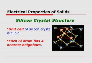


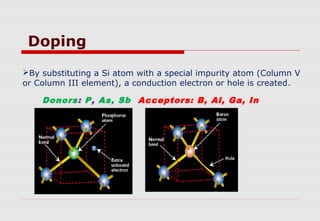


The document provides an overview of semiconductor devices, focusing on the fundamental concepts of diodes and p-n junctions, which are essential for various electronic applications. It describes the properties of semiconductors, the significance of doping in creating n-type and p-type materials, and outlines the characteristics and functioning of diodes, including forward and reverse bias operations. The document also includes insights into the fabrication processes and applications of semiconductor devices in modern technology.