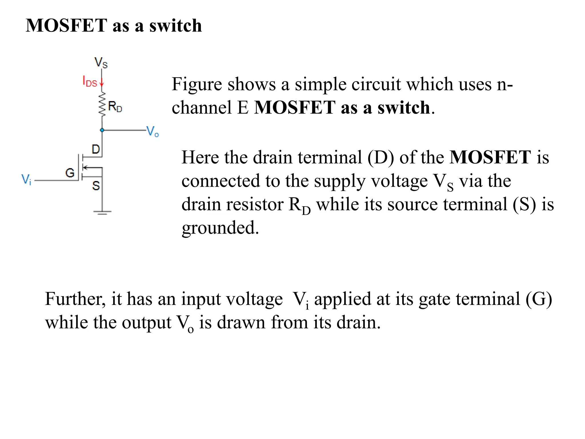
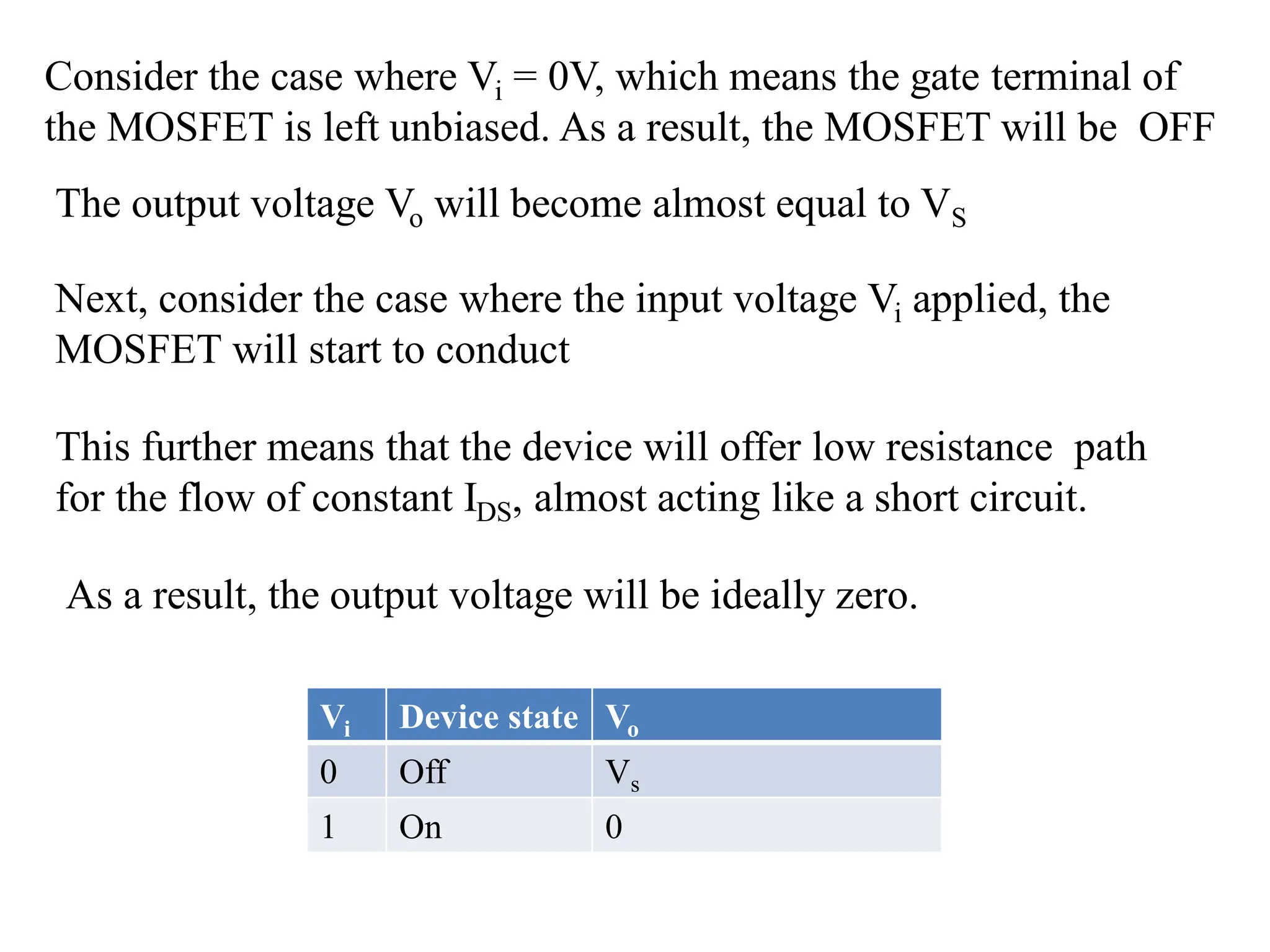
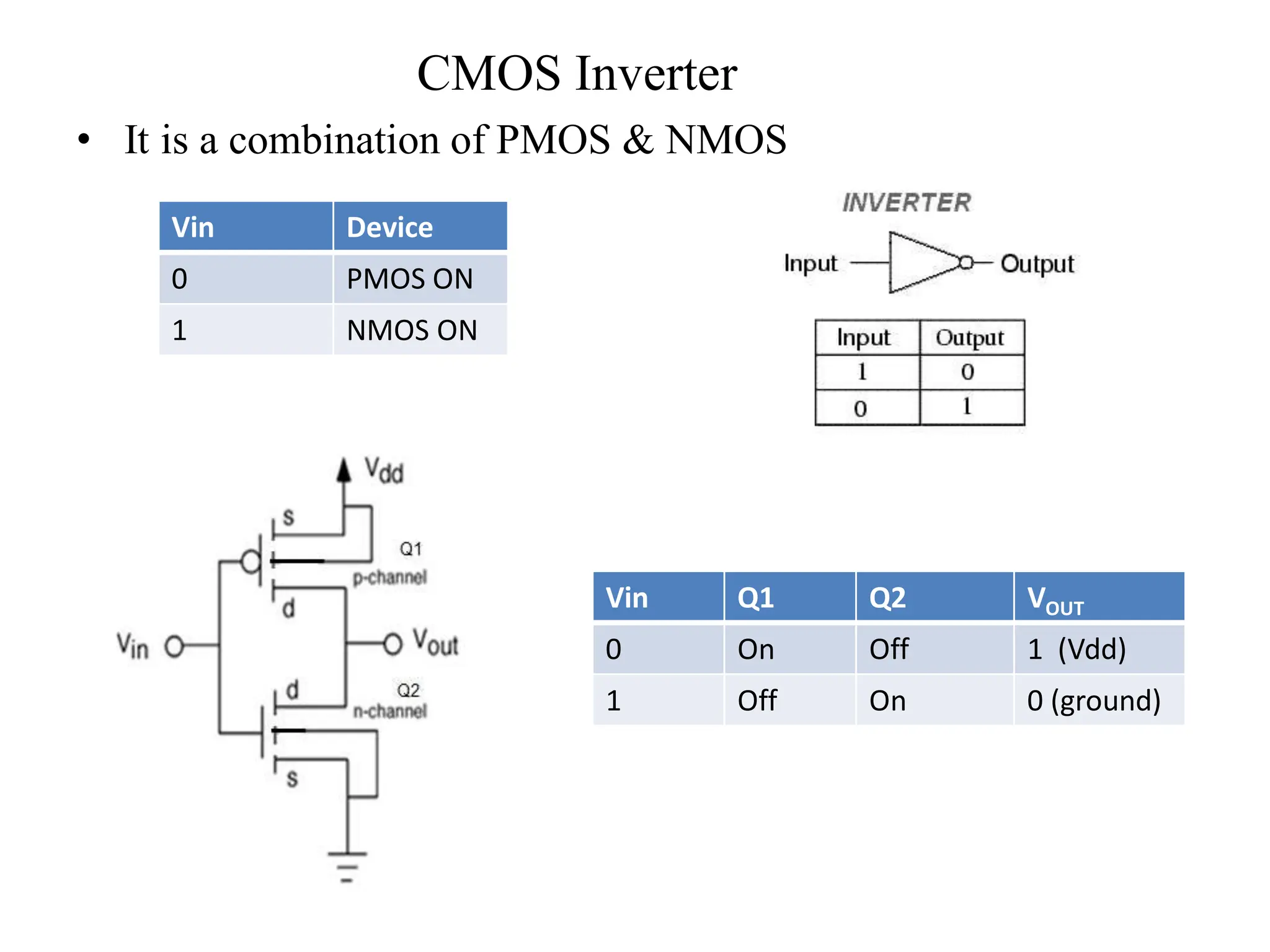
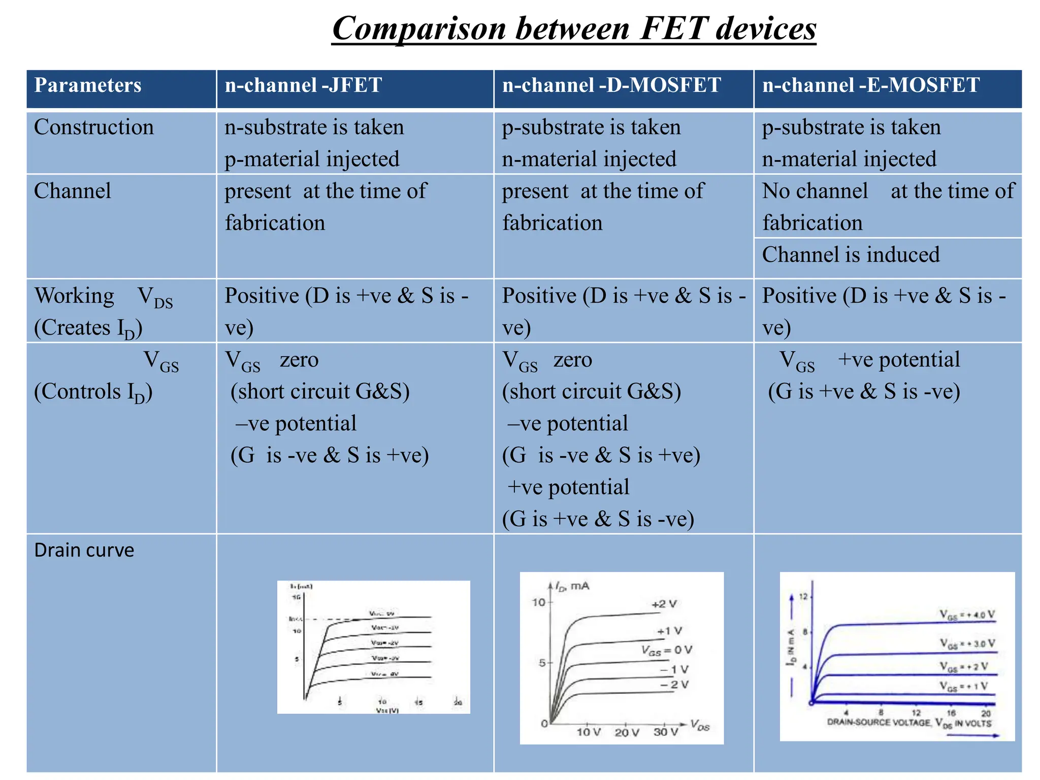
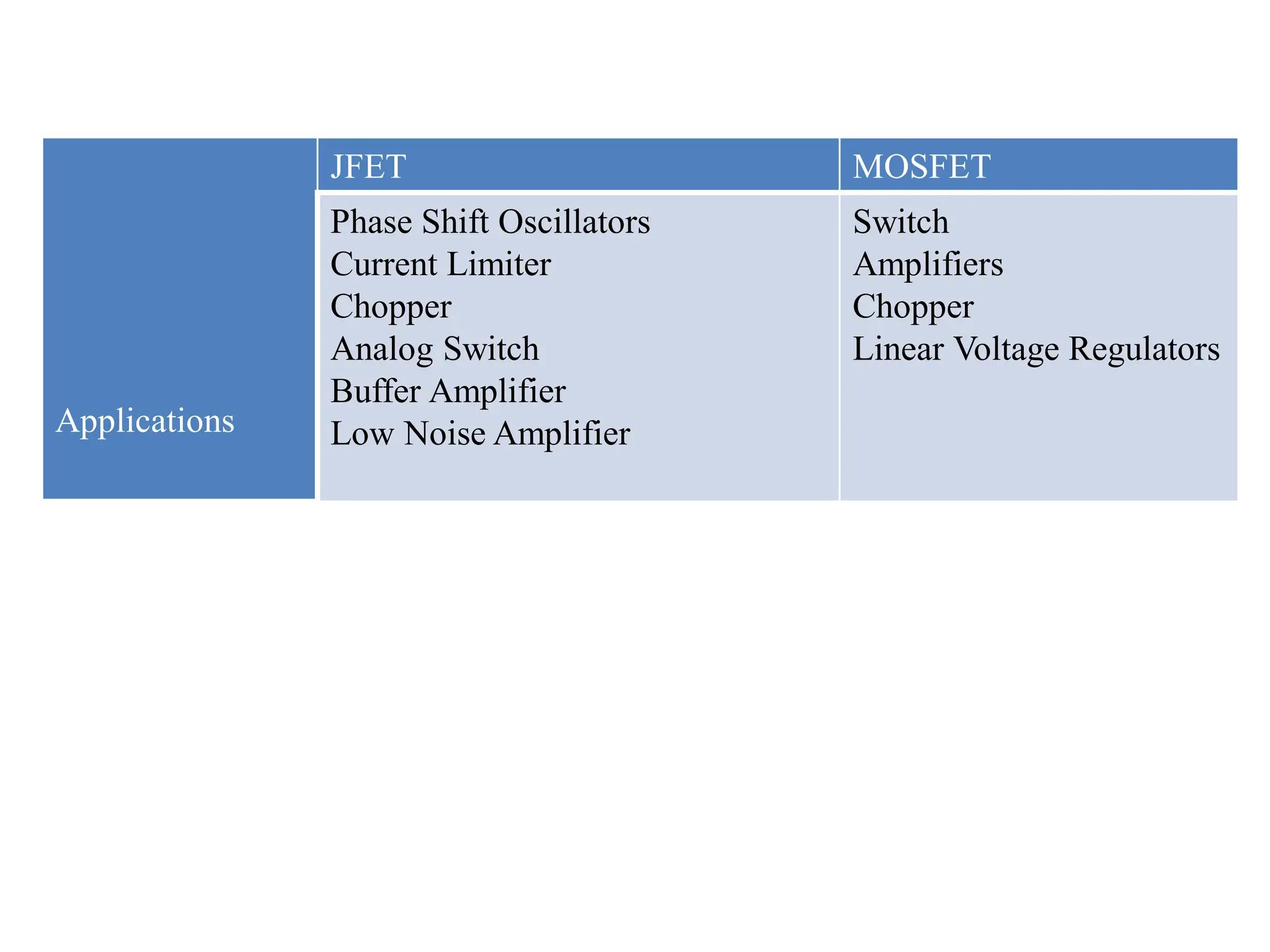
MOSFET as a switch, CMOS Inverter and
Comparison between BJT, FET and MOSFET
Figure shows a simple circuit which uses n-
channel E MOSFET as a switch.
Here the drain terminal (D) of the MOSFET is
connected to the supply voltage VS via the
drain resistor RD while its source terminal (S) is
grounded.
Further, it has an input voltage Vi applied at its gate terminal (G)
while the output Vo is drawn from its drain.
MOSFET as a switch
Consider the case where Vi = 0V, which means the gate terminal of
the MOSFET is left unbiased. As a result, the MOSFET will be OFF
The output voltage Vo will become almost equal to VS
Next, consider the case where the input voltage Vi applied, the
MOSFET will start to conduct
This further means that the device will offer low resistance path
for the flow of constant IDS, almost acting like a short circuit.
As a result, the output voltage will be ideally zero.
Vi Device state Vo
0 Off Vs
1 On 0
CMOS Inverter construction :
It is a combination of PMOS & NMOS
Gates are connected together & i/p is given
Both drains are connected together & o/p is taken
In PMOS, source is connected to supply voltage Vdd and source in
NMOS is connected to ground
CMOS Inverter
• It is a combination of PMOS & NMOS
Vin Q1 Q2 VOUT
0 On Off 1 (Vdd)
1 Off On 0 (ground)
Vin Device
0 PMOS ON
1 NMOS ON
Comparison between BJT, FET and MOSFET
TERMS BJT FET MOSFET
Device type Current controlled Voltage controlled Voltage Controlled
Current flow Bipolar Unipolar Unipolar
Terminals Not interchangeable Interchangeable Interchangeable
Operational modes No modes D mode only Both E and D modes
Input impedance Low High Very high
Output resistance Moderate Moderate Low
Operational speed Low Moderate High
Noise High Low Low
Thermal stability Low Better High
Parameters n-channel -JFET n-channel -D-MOSFET n-channel -E-MOSFET
Construction n-substrate is taken
p-material injected
p-substrate is taken
n-material injected
p-substrate is taken
n-material injected
Channel present at the time of
fabrication
present at the time of
fabrication
No channel at the time of
fabrication
Channel is induced
Working VDS
(Creates ID)
Positive (D is +ve & S is -
ve)
Positive (D is +ve & S is -
ve)
Positive (D is +ve & S is -
ve)
VGS
(Controls ID)
VGS zero
(short circuit G&S)
–ve potential
(G is -ve & S is +ve)
VGS zero
(short circuit G&S)
–ve potential
(G is -ve & S is +ve)
+ve potential
(G is +ve & S is -ve)
VGS +ve potential
(G is +ve & S is -ve)
Drain curve
Comparison between FET devices
Parameters n-channel -JFET n-channel -D-
MOSFET
n-channel -E-
MOSFET
Transfer curve
Symbol
Name Voltage Controlled Device
Applications
JFET MOSFET
Phase Shift Oscillators
Current Limiter
Chopper
Analog Switch
Buffer Amplifier
Low Noise Amplifier
Switch
Amplifiers
Chopper
Linear Voltage Regulators

MOSFET as a switch

  • 1.
    MOSFET as aswitch, CMOS Inverter and Comparison between BJT, FET and MOSFET
  • 2.
    Figure shows asimple circuit which uses n- channel E MOSFET as a switch. Here the drain terminal (D) of the MOSFET is connected to the supply voltage VS via the drain resistor RD while its source terminal (S) is grounded. Further, it has an input voltage Vi applied at its gate terminal (G) while the output Vo is drawn from its drain. MOSFET as a switch
  • 3.
    Consider the casewhere Vi = 0V, which means the gate terminal of the MOSFET is left unbiased. As a result, the MOSFET will be OFF The output voltage Vo will become almost equal to VS Next, consider the case where the input voltage Vi applied, the MOSFET will start to conduct This further means that the device will offer low resistance path for the flow of constant IDS, almost acting like a short circuit. As a result, the output voltage will be ideally zero. Vi Device state Vo 0 Off Vs 1 On 0
  • 4.
    CMOS Inverter construction: It is a combination of PMOS & NMOS Gates are connected together & i/p is given Both drains are connected together & o/p is taken In PMOS, source is connected to supply voltage Vdd and source in NMOS is connected to ground
  • 5.
    CMOS Inverter • Itis a combination of PMOS & NMOS Vin Q1 Q2 VOUT 0 On Off 1 (Vdd) 1 Off On 0 (ground) Vin Device 0 PMOS ON 1 NMOS ON
  • 6.
    Comparison between BJT,FET and MOSFET TERMS BJT FET MOSFET Device type Current controlled Voltage controlled Voltage Controlled Current flow Bipolar Unipolar Unipolar Terminals Not interchangeable Interchangeable Interchangeable Operational modes No modes D mode only Both E and D modes Input impedance Low High Very high Output resistance Moderate Moderate Low Operational speed Low Moderate High Noise High Low Low Thermal stability Low Better High
  • 7.
    Parameters n-channel -JFETn-channel -D-MOSFET n-channel -E-MOSFET Construction n-substrate is taken p-material injected p-substrate is taken n-material injected p-substrate is taken n-material injected Channel present at the time of fabrication present at the time of fabrication No channel at the time of fabrication Channel is induced Working VDS (Creates ID) Positive (D is +ve & S is - ve) Positive (D is +ve & S is - ve) Positive (D is +ve & S is - ve) VGS (Controls ID) VGS zero (short circuit G&S) –ve potential (G is -ve & S is +ve) VGS zero (short circuit G&S) –ve potential (G is -ve & S is +ve) +ve potential (G is +ve & S is -ve) VGS +ve potential (G is +ve & S is -ve) Drain curve Comparison between FET devices
  • 8.
    Parameters n-channel -JFETn-channel -D- MOSFET n-channel -E- MOSFET Transfer curve Symbol Name Voltage Controlled Device
  • 9.
    Applications JFET MOSFET Phase ShiftOscillators Current Limiter Chopper Analog Switch Buffer Amplifier Low Noise Amplifier Switch Amplifiers Chopper Linear Voltage Regulators