Downloaded 5,484 times

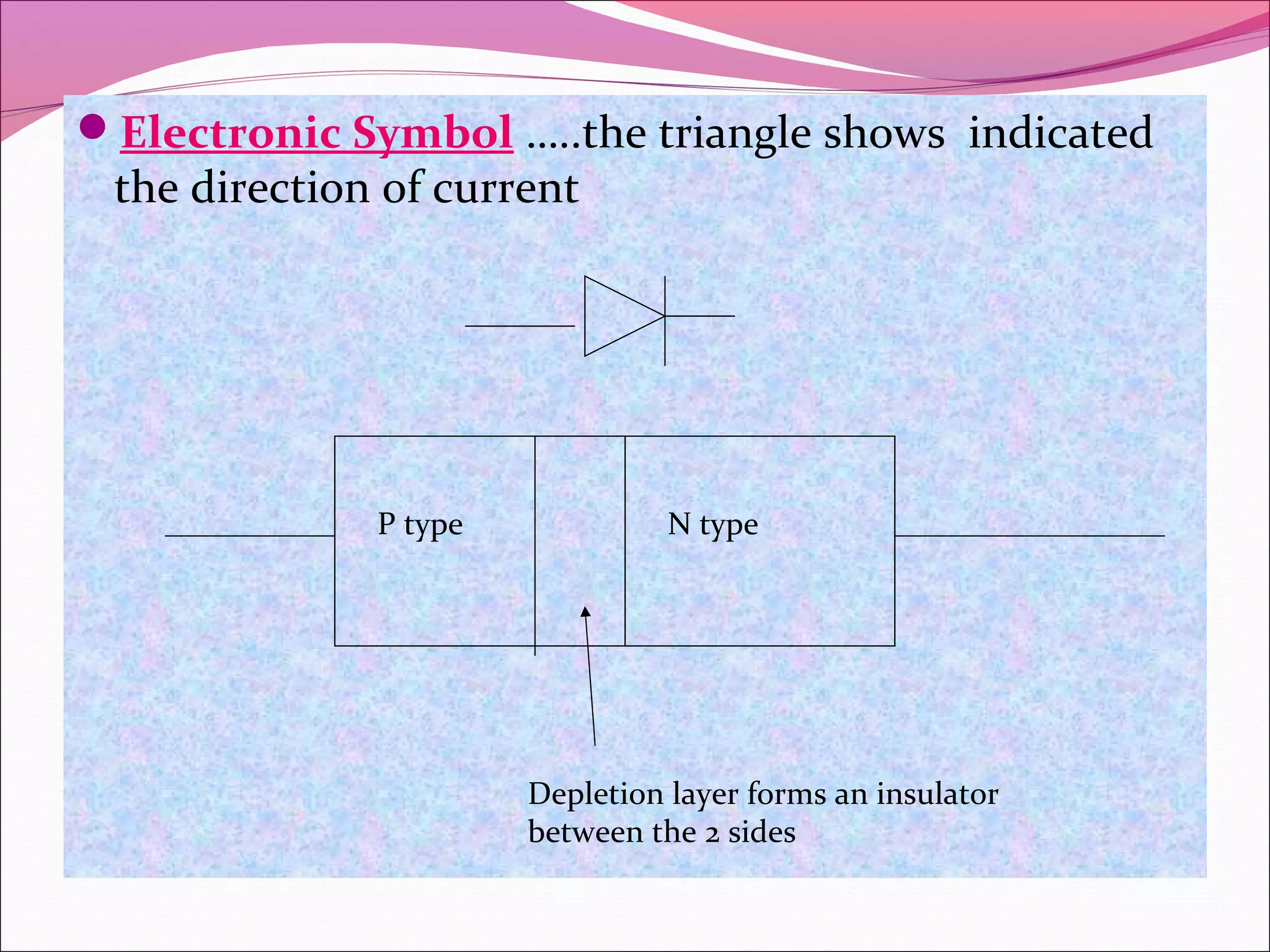

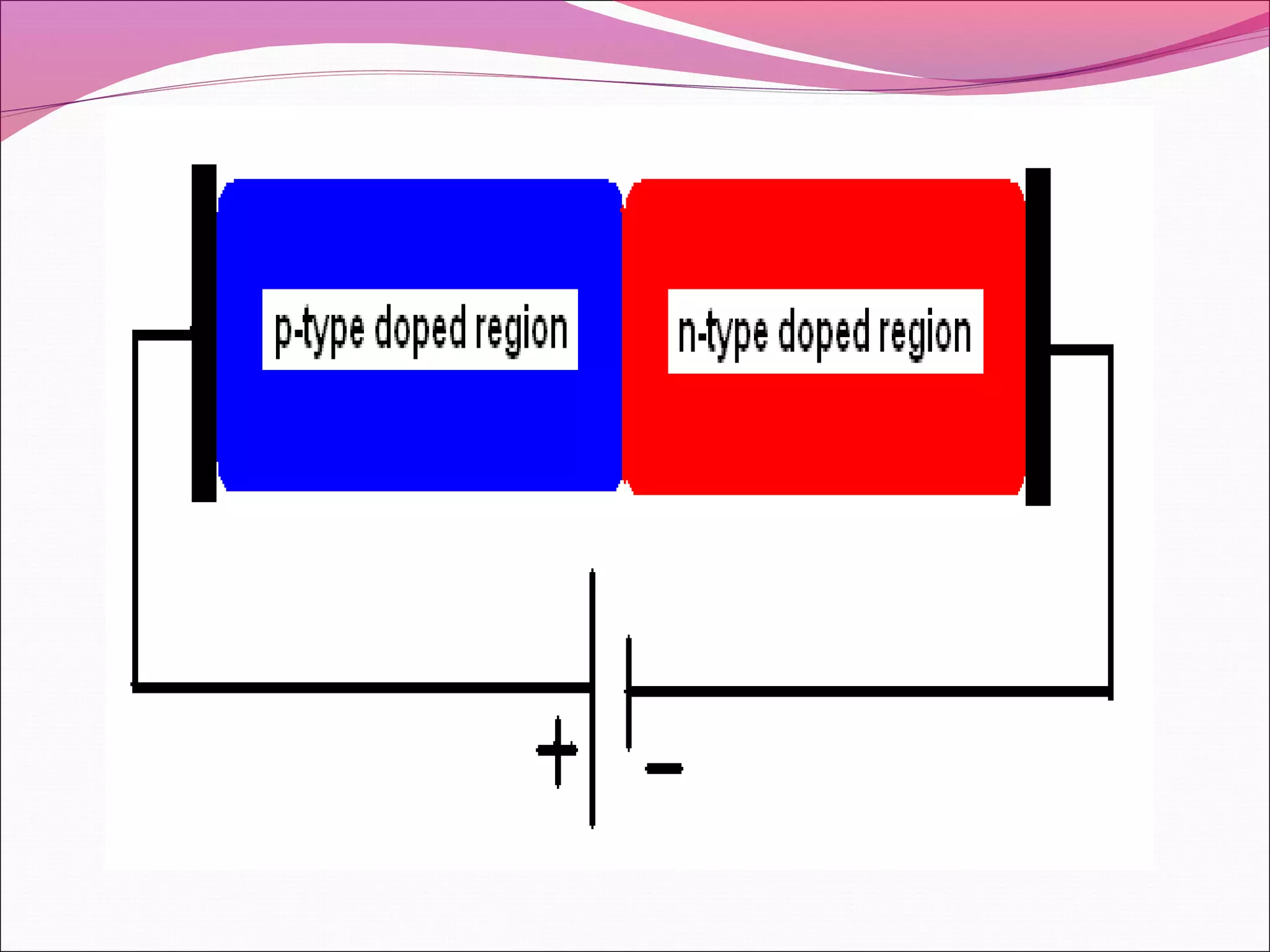


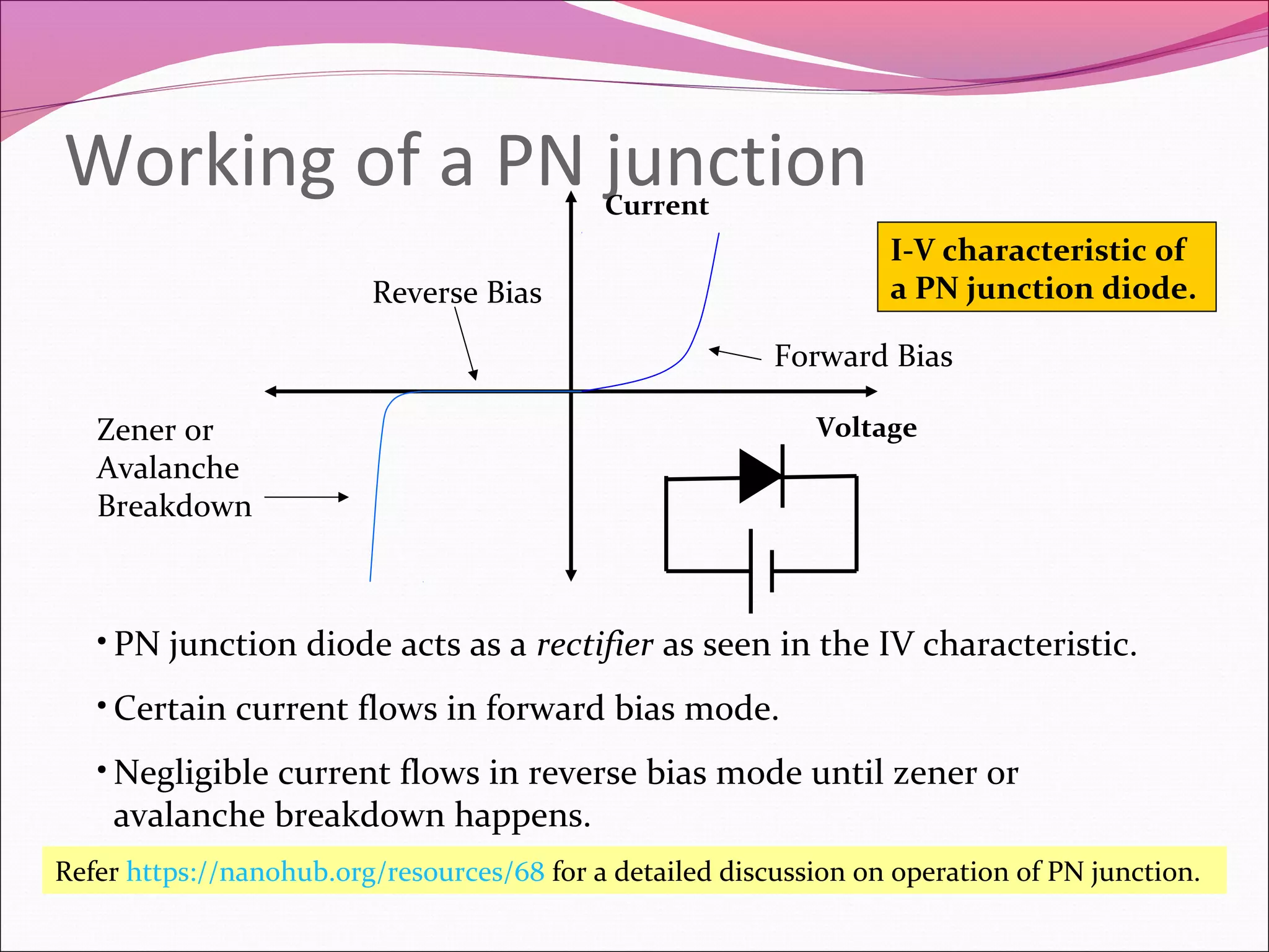


A PN junction is formed by joining a P-type semiconductor with an N-type semiconductor. When joined, a depletion layer forms at the junction that acts as an insulator. When forward biased, current flows easily through the junction. When reverse biased, very little current flows due to the high resistance of the depletion layer acting as a barrier. PN junction diodes are used as rectifiers, switches, detectors, and light emitting diodes (LEDs) in electronic circuits.


![ppt on IC [Integrated Circuit]](https://cdn.slidesharecdn.com/ss_thumbnails/1-171227170055-thumbnail.jpg?width=640&height=640&fit=bounds)