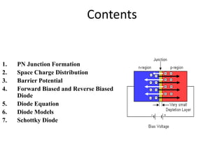
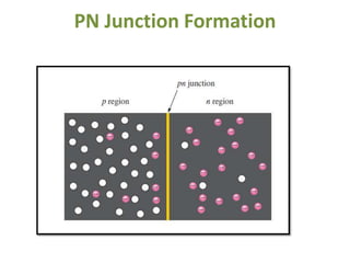
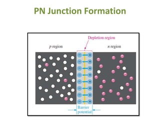
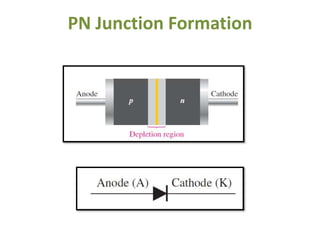
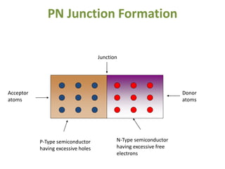
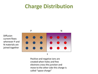
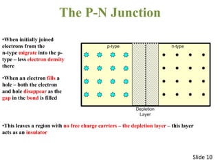
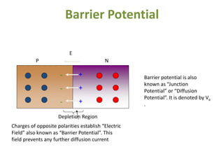
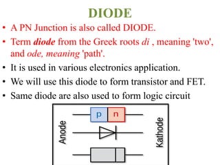
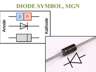
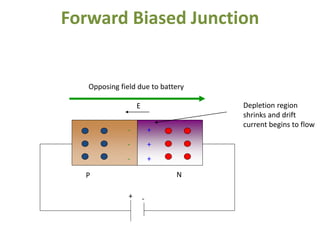
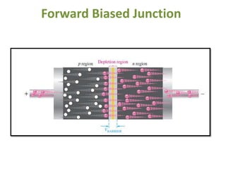
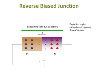
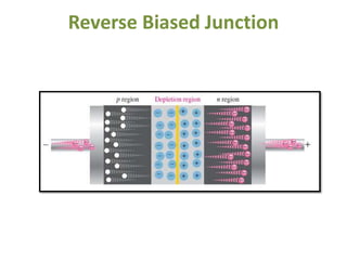
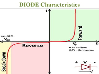
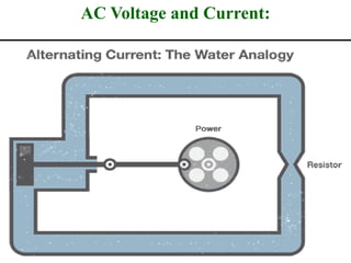
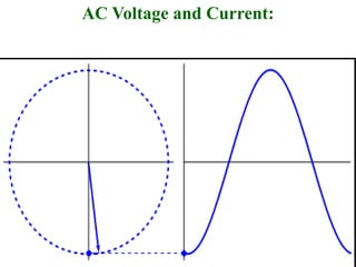
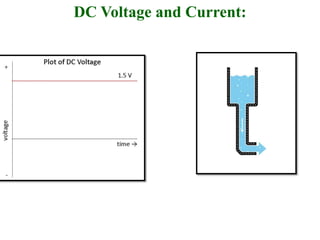
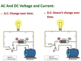
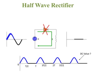
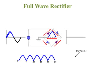
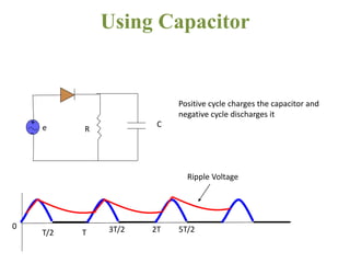
Basic Electronics
Lecture#6
PN Junction, Diode/
Diode Application.
By: sarmad baloch
Class of BS.IT, ISP
P-N Junction
Contents
1. PN Junction Formation
2. Space Charge Distribution
3. Barrier Potential
4. Forward Biased and Reverse Biased
Diode
5. Diode Equation
6. Diode Models
7. Schottky Diode
PN Junction Formation
P-Type semiconductor
having excessive holes
N-Type semiconductor
having excessive free
electrons
Junction
Acceptor
atoms
Donor
atoms
Charge Distribution
P N
+
+
+
-
-
-
Positive and negative ions are
created when holes and free
electrons cross the junction and
move to the other side this charge is
called “space charge”
Diffusion
current flows
whenever P and
N materials are
joined together
The P-N Junction
•When initially joined
electrons from the
n-type migrate into the p-
type – less electron density
there
•When an electron fills a
hole – both the electron
and hole disappear as the
gap in the bond is filled
•This leaves a region with no free charge carriers – the depletion layer – this layer
acts as an insulator
Slide 10
Barrier Potential
P N
+
+
+
-
-
-
Charges of opposite polarities establish “Electric
Field” also known as “Barrier Potential”. This
field prevents any further diffusion current
E
Depletion Region
Barrier potential is also
known as “Junction
Potential” or “Diffusion
Potential”. It is denoted by Vo
.
Barrier Potential
• Silicon has potential barrier drop of
0.7V.
• Germanium has potential barrier
voltage drop of 0.3V.
DIODE
(Formed Using P-N Junction)
DIODE
• A PN Junction is also called DIODE.
• Term diode from the Greek roots di , meaning 'two',
and ode, meaning 'path'.
• It is used in various electronics application.
• We will use this diode to form transistor and FET.
• Same diode are also used to form logic circuit
DIODE SYMBOL, SIGN
Forward Biased Junction
+
+
+
-
-
-
E
NP
+ -
Opposing field due to battery
Depletion region
shrinks and drift
current begins to flow
Forward Biased Junction
Reverse Biased Junction
+
+
+
-
-
-
E
NP
+-
Supporting field due to battery
Depletion region
expands and opposes
flow of current
Reverse Biased Junction
DIODE Characteristics
To Remember!
•Diode cannot conduct in reverse bias condition.
•Diode can conduct in forward bias condition.
•Silicon diode has voltage drop of 0.7V
•Germanium has voltage drop of 0.3V
DIODE APPLICATION
RECTIFIER OR AC TO DC
CONVERSION
AC Voltage and Current:
DC Voltage and Current:
AC And DC Voltage and Current:
 A.C: Change over time.  D.C: Doesn't change over
time.
Half Wave Rectifier
+
- Re
0
T/2 T 3T/2 2T 5T/2
DC Value ?
Full Wave Rectifier
+
-
0 T 2T 3T 4T 5T
DC Value ?
Using Capacitor
+
- Re C
0
T/2 T 3T/2 2T 5T/2
Positive cycle charges the capacitor and
negative cycle discharges it
Ripple Voltage
DC Output With Capacitor
0 T 2T 3T 4T 5T
+
-
R
C
Vac
Load
Full-wave rectifier circuit
• Bridge circuit
• Load
– Circuit requiring DC
Ripple Voltage
0 T/2 T 3T/2 2T 5T/2
Ripple Voltage
0 T/2 T 3T/2 2T 5T/2
Ripple Voltage
VDC VPP
VPR
Pn junction diode by sarmad baloch

Pn junction diode by sarmad baloch