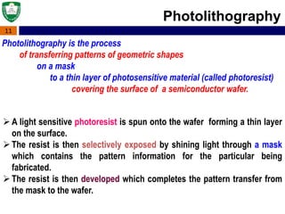
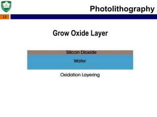
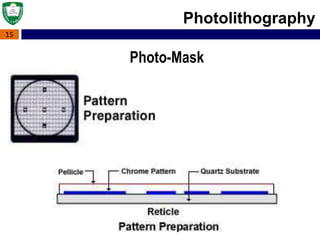
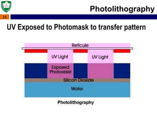
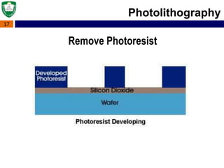
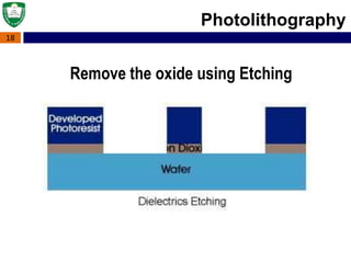
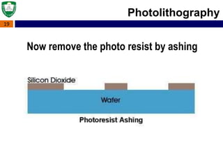
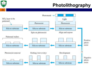
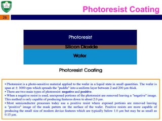
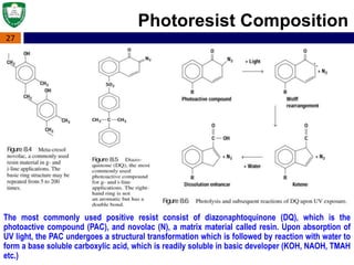
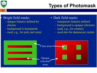
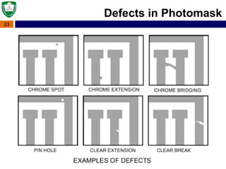
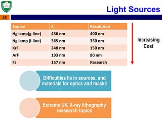
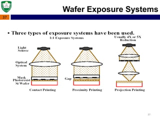
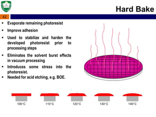
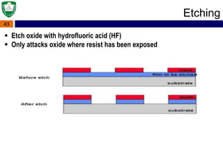
Lithography
Instructor
Abu Syed Md. Jannatul Islam
Lecturer, Dept. of EEE, KUET, BD
1
Department of Electrical and Electronic Engineering
Khulna University of Engineering & Technology
Khulna-9203
2
Electrical and mechanical properties of the wafer depend on the orientation of the crystalline
structure, the impurity concentrations, and the type of impurities present.
The surface of the wafer is then polished to a mirror finish using chemical and mechanical
polishing (CMP) techniques.
Crystal is then sawed (like a loaf of bread) to produce circular wafers that are 400μm to 600μm
thick
Solid cylinder 10 cm to 30 cm in diameter and can be 1 to 2 m in length.
Very-high-purity, single-crystal silicon ingot
Basic Things
3
When designating the relative doping concentrations in semiconductor material, it is common
to use the + and – symbols.
If a large number of impurity atoms is added, the silicon will be heavily doped (e.g.,
concentration > ∼10^18 atoms/cm−3).
Depending on the types of impurity, either holes (in p-type silicon) or electrons (in n-type
silicon) can be responsible for electrical conduction.
A specific amount of impurities known as doping allows the alteration of the electrical
properties of the silicon, in particular its resistivity.
These variables are strictly controlled during crystal growth
Basic Things
4
The ability to control the type of impurities and the doping concentration in the silicon permits
the formation of diodes, transistors, and resistors in integrated circuits.
Similarly, p+ and p− designations refer to the heavily doped and lightly doped p-type regions,
respectively.
A heavily doped (low-resistivity) n-type silicon wafer is referred to as n+ material, while a lightly
doped material (e.g., concentration < ∼1016 atoms/cm−3) is referred to as n−.
Basic Things
5
 Simple layers of thin films do not make a Device.
Why Lithography?
6
Why Lithography?
7
 It was invented in 1796 by German author and
actor Alois Senefelder as a cheap method of
publishing theatrical works.
History of Lithography
8
What is Lithography ?
Lithography comes from two Greek words,
“lithos” which means stone and “graphein” which
means write.
“ writing a pattern on stone”
 Lithography is the transfer of geometric shapes on a mask
to a smooth surface
 It uses light or other forms of radiant energy to change the
chemical properties of thin layers of films that have been
coated on a substrate.
 Typically 8-25 lithography steps and several hundred
processing steps between exposure are required to
fabricate a packed IC.
9
Lithography is one of the 4 major processes in the top-down
model
 Lithography
 Etching
 Deposition
 Doping
What is lithography ?
In order to perform the other 3 processes,
we must precisely define where to do them
Lithography Does This!
10
 Photolithography
 E-beam lithography
 X-ray lithography.
 Interference lithography.
 Scanning Probe lithography
Types of Lithography
11
Photolithography is the process
of transferring patterns of geometric shapes
on a mask
to a thin layer of photosensitive material (called photoresist)
covering the surface of a semiconductor wafer.
Photolithography
A light sensitive photoresist is spun onto the wafer forming a thin layer
on the surface.
The resist is then selectively exposed by shining light through a mask
which contains the pattern information for the particular being
fabricated.
The resist is then developed which completes the pattern transfer from
the mask to the wafer.
12
Photolithography is an optical means for transferring patterns
onto a substrate
Overview of the Photolithography Process
1. Surface Preparation (Get rid of H2O, RCA clean, apply adhesion
promoter
2. Deposit (Photoresist Coating by Spin Casting)
3. Soft Bake (90 – 120°C for 60 –120 sec to remove solvent from liquid
photoresist
4. Photo Mask Alignment
5. Exposure (Pattern transfer)
6. Development (Remove soluble photoresist)
7. Hard Bake (100 – 180°C) to increase adhesion
8. Etching (Remove oxide)
9. Stripping (Photoresist removal)
10. Post Processing/Cleaning (Ashing)
Photolithography
13
Photolithography
Grow Oxide Layer
14
Photolithography
Add Photoresist
15
Photolithography
Photo-Mask
16
Photolithography
UV Exposed to Photomask to transfer pattern
17
Photolithography
Remove Photoresist
18
Photolithography
Remove the oxide using Etching
19
Photolithography
Now remove the photo resist by ashing
20
Photolithography
Diffuse new region by
ion implantation or diffusion
21
Photolithography
22
Photolithography
23
The surface patterns of the various integrated-circuit components
can be defined repeatedly using photolithography
Here, a photographic plate with drawn patterns will be used to
selectively expose the photoresist under a deep ultraviolet
illumination (UV)
The exposed areas will become softened (for positive photoresist)
The exposed layer can then be removed using a chemical developer,
causing the mask pattern to be duplicated on the wafer
Silicon dioxide, silicon nitride, polysilicon, and metal layers can be
selectively removed using the appropriate etching methods
After the etching step(s), the photoresist is stripped away, leaving
behind a permanent pattern of the photomask on the wafer surface
Photolithography
24
Photolithography
25
Photoresist Coating
The wafer surface is coated with a
photosensitive layer called photoresist,
using a spin-on technique
26
Photoresist Coating
27
Photoresist Composition
The most commonly used positive resist consist of diazonaphtoquinone (DQ), which is the
photoactive compound (PAC), and novolac (N), a matrix material called resin. Upon absorption of
UV light, the PAC undergoes a structural transformation which is followed by reaction with water to
form a base soluble carboxylic acid, which is readily soluble in basic developer (KOH, NAOH, TMAH
etc.)
28
Positive Photoresist
 Most commonly used in
the IC industry.
 Become soluble after
exposure
 Better resolution
 Cheaper
Negative Photoresist
 Becomes insoluble after
exposure
 When developed, the
unexposed parts
dissolved
 Cheaper
Types of Photoresist
29
Soft Bake
 Used to evaporate the coating solvent and to densify the
resist after spin coating.
 Typical thermal cycles: 90-100°C for 20 min. in a
convection oven, 75-85°C for 45 sec. on a hot plate
 Commercially, microwave heating or IR lamps are also
used in production lines.
 Improves adhesion
 Improves uniformity
 Improves etch resistance
 Improves line width control
 Optimizes light absorbance characteristics of photoresist
30
 Photomasks are high precision plates containing microscopic images
of electronic circuits.
 There are four types of material used to make photomasks;
 quartz (the most commonly used and most expensive), LE, soda lime,
and white crown.
What Is a Photomask?
Material Used to make Photomasks:
31
Types of Photomask
32
15 – 20 different mask levels are
typically required for a complete IC
process
Different Photomasks
33
Defects in Photomask
34
Photomask Aligner
35
Light Sources
Source λ Resolution
Hg lamp(g-line) 436 nm 400 nm
Hg lamp (i-line) 365 nm 350 nm
KrF 248 nm 150 nm
ArF 193 nm 80 nm
F2 157 nm Research
Difficulties lie in sources, and
materials for optics and masks
Extreme UV, X-ray lithography
reasearch topics
Increasing
Cost
36
36
Wafer Exposure Systems
37
37
Wafer Exposure Systems
38
Contact Printing
 The mask is directly in contact with
the wafer
 Advantages
 Simple
 Low Cost
 Disadvantages
 Poor for small features
 Mask damage may occur from
contact
 Defects from contaminants on
mask or wafer due to contacting
surfaces
39
Proximity Printing
 The mask is above the wafer surface
 Advantages
 Mask damage is minimal
 Good registration possible
 Disadvantages
 Poorer resolution due to distance
from the surface
 Diffraction errors
40
Projection Printing
 An optical system focuses the
light source and reduces the
mask image for exposure on
the surface
 Advantages
 Higher resolution
 Lens system reduces
diffraction error
 Disadvantages
 Errors due to focus of lens
system may occur
 Limiting factor in resolution
can be due to optical
system
41
to vacuum
pump
vacuum chuck
spindle
developer
dispenser
Develop
 Soluble areas of photoresist are dissolved by developer chemical
 Visible patterns appear on wafer
 windows
 islands
42
Hard Bake
 Evaporate remaining photoresist
 Improve adhesion
 Used to stabilize and harden the
developed photoresist prior to
processing steps
 Eliminates the solvent burst effects
in vacuum processing
 Introduces some stress into the
photoresist.
 Needed for acid etching, e.g. BOE.
43
Etching
 Etch oxide with hydrofluoric acid (HF)
 Only attacks oxide where resist has been exposed
44
 Want to remove the photoresist and any of its residues.
– Positive photoresists:
• acetone
• trichloroethylene (TCE)
• phenol-based strippers
– Negative photoresists:
• methyl ethyl ketone (MEK), CH3COC2H5
• methyl isobutyl ketone (MIBK), CH3COC4H9
Photoresist Removal (Stripping)
Plasma etching with O2 (Ashing) is also effective for
removing organic polymer debris.
45
 Resolution: minimum feature dimension that can be transferred with
high fidelity to a resist film.
 Registration: how accurately patterns on successive masks can be
aligned (or overlaid) with respect to previously defined patterns.
 Throughput: number of wafers that can be exposed/unit time for a
given mask level.
Performance Metrics
46
Limitations of Optical Lithography
 Resolution becoming a challenge for deep-submicron IC process
requirements
 Complexity of mask production and mask inspection
 High cost of masks
47
Electron Beam Lithography
• Involves direct exposure of the resist by a focused electron
beam without a mask
• Resolution as low as 10 – 25 nm
48
 Electron gun
generates beam of
electrons
 Condenser lenses
focus the e-beam
 Beam-blanking
plates turn beam
on and off
Electron Beam Lithography
49
Electron Beam Lithography
Advantages
 Generation of submicron resist geometries
 Highly automated and precisely controlled operation
 Greater depth of focus than that available from optical lithography
 Direct patterning on wafer without using a mask
Disadvantages
 Low throughput
 Expensive resists
 Proximity effect: backscattering of electrons irradiates adjacent regions
and limits minimum spacing between features
50
50
Extreme ultraviolet : EUV
 Vacuum operation
 Laser plasma source
 Very expensive system
 Uses very short 13.4 nm light
 Step and scan printing
 All reflective optics (at this wavelength all materials absorb!)
 Uses reduction optics (4X)
 Optical tricks seen before all apply: off axis illumination
(OAI), phase shift masks and OPC
Next Generation Lithography
51
51
Extreme ultraviolet : EUV
Challenges:
• EUV is strongly absorbed in all materials.
• Lithography process must be performed in vacuum
• Mask blank must also be multilayer coated to minimize its reflection.
52
52
1nmAdvantages:
 Low diffraction
 Shorter exposure time
 Scattering is minimum
 X –rays pass through spots
Problems:
 Masks are the most
 Difficult and critical
 Element of an XRL system
 lacking of photoresist
 1:1 printing
 High energy x-ray destroy
conventional optics
X-ray Lithography
53
53
X-ray Lithography

Lithography, Photolithography--ABU SYED KUET

  • 1.
    Lithography Instructor Abu Syed Md.Jannatul Islam Lecturer, Dept. of EEE, KUET, BD 1 Department of Electrical and Electronic Engineering Khulna University of Engineering & Technology Khulna-9203
  • 2.
    2 Electrical and mechanicalproperties of the wafer depend on the orientation of the crystalline structure, the impurity concentrations, and the type of impurities present. The surface of the wafer is then polished to a mirror finish using chemical and mechanical polishing (CMP) techniques. Crystal is then sawed (like a loaf of bread) to produce circular wafers that are 400μm to 600μm thick Solid cylinder 10 cm to 30 cm in diameter and can be 1 to 2 m in length. Very-high-purity, single-crystal silicon ingot Basic Things
  • 3.
    3 When designating therelative doping concentrations in semiconductor material, it is common to use the + and – symbols. If a large number of impurity atoms is added, the silicon will be heavily doped (e.g., concentration > ∼10^18 atoms/cm−3). Depending on the types of impurity, either holes (in p-type silicon) or electrons (in n-type silicon) can be responsible for electrical conduction. A specific amount of impurities known as doping allows the alteration of the electrical properties of the silicon, in particular its resistivity. These variables are strictly controlled during crystal growth Basic Things
  • 4.
    4 The ability tocontrol the type of impurities and the doping concentration in the silicon permits the formation of diodes, transistors, and resistors in integrated circuits. Similarly, p+ and p− designations refer to the heavily doped and lightly doped p-type regions, respectively. A heavily doped (low-resistivity) n-type silicon wafer is referred to as n+ material, while a lightly doped material (e.g., concentration < ∼1016 atoms/cm−3) is referred to as n−. Basic Things
  • 5.
    5  Simple layersof thin films do not make a Device. Why Lithography?
  • 6.
  • 7.
    7  It wasinvented in 1796 by German author and actor Alois Senefelder as a cheap method of publishing theatrical works. History of Lithography
  • 8.
    8 What is Lithography? Lithography comes from two Greek words, “lithos” which means stone and “graphein” which means write. “ writing a pattern on stone”  Lithography is the transfer of geometric shapes on a mask to a smooth surface  It uses light or other forms of radiant energy to change the chemical properties of thin layers of films that have been coated on a substrate.  Typically 8-25 lithography steps and several hundred processing steps between exposure are required to fabricate a packed IC.
  • 9.
    9 Lithography is oneof the 4 major processes in the top-down model  Lithography  Etching  Deposition  Doping What is lithography ? In order to perform the other 3 processes, we must precisely define where to do them Lithography Does This!
  • 10.
    10  Photolithography  E-beamlithography  X-ray lithography.  Interference lithography.  Scanning Probe lithography Types of Lithography
  • 11.
    11 Photolithography is theprocess of transferring patterns of geometric shapes on a mask to a thin layer of photosensitive material (called photoresist) covering the surface of a semiconductor wafer. Photolithography A light sensitive photoresist is spun onto the wafer forming a thin layer on the surface. The resist is then selectively exposed by shining light through a mask which contains the pattern information for the particular being fabricated. The resist is then developed which completes the pattern transfer from the mask to the wafer.
  • 12.
    12 Photolithography is anoptical means for transferring patterns onto a substrate Overview of the Photolithography Process 1. Surface Preparation (Get rid of H2O, RCA clean, apply adhesion promoter 2. Deposit (Photoresist Coating by Spin Casting) 3. Soft Bake (90 – 120°C for 60 –120 sec to remove solvent from liquid photoresist 4. Photo Mask Alignment 5. Exposure (Pattern transfer) 6. Development (Remove soluble photoresist) 7. Hard Bake (100 – 180°C) to increase adhesion 8. Etching (Remove oxide) 9. Stripping (Photoresist removal) 10. Post Processing/Cleaning (Ashing) Photolithography
  • 13.
  • 14.
  • 15.
  • 16.
    16 Photolithography UV Exposed toPhotomask to transfer pattern
  • 17.
  • 18.
  • 19.
    19 Photolithography Now remove thephoto resist by ashing
  • 20.
    20 Photolithography Diffuse new regionby ion implantation or diffusion
  • 21.
  • 22.
  • 23.
    23 The surface patternsof the various integrated-circuit components can be defined repeatedly using photolithography Here, a photographic plate with drawn patterns will be used to selectively expose the photoresist under a deep ultraviolet illumination (UV) The exposed areas will become softened (for positive photoresist) The exposed layer can then be removed using a chemical developer, causing the mask pattern to be duplicated on the wafer Silicon dioxide, silicon nitride, polysilicon, and metal layers can be selectively removed using the appropriate etching methods After the etching step(s), the photoresist is stripped away, leaving behind a permanent pattern of the photomask on the wafer surface Photolithography
  • 24.
  • 25.
    25 Photoresist Coating The wafersurface is coated with a photosensitive layer called photoresist, using a spin-on technique
  • 26.
  • 27.
    27 Photoresist Composition The mostcommonly used positive resist consist of diazonaphtoquinone (DQ), which is the photoactive compound (PAC), and novolac (N), a matrix material called resin. Upon absorption of UV light, the PAC undergoes a structural transformation which is followed by reaction with water to form a base soluble carboxylic acid, which is readily soluble in basic developer (KOH, NAOH, TMAH etc.)
  • 28.
    28 Positive Photoresist  Mostcommonly used in the IC industry.  Become soluble after exposure  Better resolution  Cheaper Negative Photoresist  Becomes insoluble after exposure  When developed, the unexposed parts dissolved  Cheaper Types of Photoresist
  • 29.
    29 Soft Bake  Usedto evaporate the coating solvent and to densify the resist after spin coating.  Typical thermal cycles: 90-100°C for 20 min. in a convection oven, 75-85°C for 45 sec. on a hot plate  Commercially, microwave heating or IR lamps are also used in production lines.  Improves adhesion  Improves uniformity  Improves etch resistance  Improves line width control  Optimizes light absorbance characteristics of photoresist
  • 30.
    30  Photomasks arehigh precision plates containing microscopic images of electronic circuits.  There are four types of material used to make photomasks;  quartz (the most commonly used and most expensive), LE, soda lime, and white crown. What Is a Photomask? Material Used to make Photomasks:
  • 31.
  • 32.
    32 15 – 20different mask levels are typically required for a complete IC process Different Photomasks
  • 33.
  • 34.
  • 35.
    35 Light Sources Source λResolution Hg lamp(g-line) 436 nm 400 nm Hg lamp (i-line) 365 nm 350 nm KrF 248 nm 150 nm ArF 193 nm 80 nm F2 157 nm Research Difficulties lie in sources, and materials for optics and masks Extreme UV, X-ray lithography reasearch topics Increasing Cost
  • 36.
  • 37.
  • 38.
    38 Contact Printing  Themask is directly in contact with the wafer  Advantages  Simple  Low Cost  Disadvantages  Poor for small features  Mask damage may occur from contact  Defects from contaminants on mask or wafer due to contacting surfaces
  • 39.
    39 Proximity Printing  Themask is above the wafer surface  Advantages  Mask damage is minimal  Good registration possible  Disadvantages  Poorer resolution due to distance from the surface  Diffraction errors
  • 40.
    40 Projection Printing  Anoptical system focuses the light source and reduces the mask image for exposure on the surface  Advantages  Higher resolution  Lens system reduces diffraction error  Disadvantages  Errors due to focus of lens system may occur  Limiting factor in resolution can be due to optical system
  • 41.
    41 to vacuum pump vacuum chuck spindle developer dispenser Develop Soluble areas of photoresist are dissolved by developer chemical  Visible patterns appear on wafer  windows  islands
  • 42.
    42 Hard Bake  Evaporateremaining photoresist  Improve adhesion  Used to stabilize and harden the developed photoresist prior to processing steps  Eliminates the solvent burst effects in vacuum processing  Introduces some stress into the photoresist.  Needed for acid etching, e.g. BOE.
  • 43.
    43 Etching  Etch oxidewith hydrofluoric acid (HF)  Only attacks oxide where resist has been exposed
  • 44.
    44  Want toremove the photoresist and any of its residues. – Positive photoresists: • acetone • trichloroethylene (TCE) • phenol-based strippers – Negative photoresists: • methyl ethyl ketone (MEK), CH3COC2H5 • methyl isobutyl ketone (MIBK), CH3COC4H9 Photoresist Removal (Stripping) Plasma etching with O2 (Ashing) is also effective for removing organic polymer debris.
  • 45.
    45  Resolution: minimumfeature dimension that can be transferred with high fidelity to a resist film.  Registration: how accurately patterns on successive masks can be aligned (or overlaid) with respect to previously defined patterns.  Throughput: number of wafers that can be exposed/unit time for a given mask level. Performance Metrics
  • 46.
    46 Limitations of OpticalLithography  Resolution becoming a challenge for deep-submicron IC process requirements  Complexity of mask production and mask inspection  High cost of masks
  • 47.
    47 Electron Beam Lithography •Involves direct exposure of the resist by a focused electron beam without a mask • Resolution as low as 10 – 25 nm
  • 48.
    48  Electron gun generatesbeam of electrons  Condenser lenses focus the e-beam  Beam-blanking plates turn beam on and off Electron Beam Lithography
  • 49.
    49 Electron Beam Lithography Advantages Generation of submicron resist geometries  Highly automated and precisely controlled operation  Greater depth of focus than that available from optical lithography  Direct patterning on wafer without using a mask Disadvantages  Low throughput  Expensive resists  Proximity effect: backscattering of electrons irradiates adjacent regions and limits minimum spacing between features
  • 50.
    50 50 Extreme ultraviolet :EUV  Vacuum operation  Laser plasma source  Very expensive system  Uses very short 13.4 nm light  Step and scan printing  All reflective optics (at this wavelength all materials absorb!)  Uses reduction optics (4X)  Optical tricks seen before all apply: off axis illumination (OAI), phase shift masks and OPC Next Generation Lithography
  • 51.
    51 51 Extreme ultraviolet :EUV Challenges: • EUV is strongly absorbed in all materials. • Lithography process must be performed in vacuum • Mask blank must also be multilayer coated to minimize its reflection.
  • 52.
    52 52 1nmAdvantages:  Low diffraction Shorter exposure time  Scattering is minimum  X –rays pass through spots Problems:  Masks are the most  Difficult and critical  Element of an XRL system  lacking of photoresist  1:1 printing  High energy x-ray destroy conventional optics X-ray Lithography
  • 53.