Downloaded 126 times
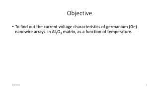
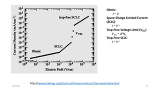
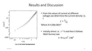
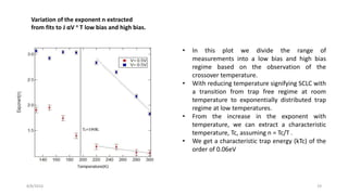
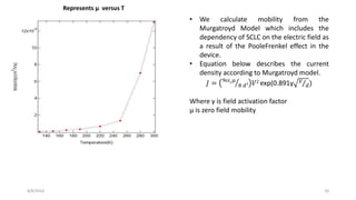
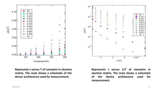
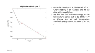
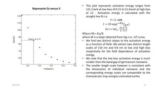


The document summarizes research on understanding charge transport in low dimensional semiconductor nanostructures embedded in an insulating matrix. Specifically, it examines current-voltage characteristics of germanium nanowire arrays in an alumina matrix as a function of temperature. Key findings include: 1) At room temperature, conduction follows Ohm's law at low voltages and Mott-Gurney's space charge limited current law at higher voltages. 2) With decreasing temperature, conduction transitions from a trap-free regime to an exponentially distributed trap regime. 3) Mobility decreases with decreasing temperature, and activation energy is extracted from an Arrhenius plot, found to be 85 meV at low temperatures and 301 meV


![Thin_Film_Technology_introduction[1]](https://cdn.slidesharecdn.com/ss_thumbnails/1b4496c8-2102-411b-8465-a3dd3f398327-150205034538-conversion-gate02-thumbnail.jpg?width=640&height=640&fit=bounds)