Downloaded 426 times


Molecular beam epitaxy (MBE) is a precise technique for growing thin crystalline layers on substrates, utilizing ultra-high vacuum and controlled molecular beams for deposition. It features in situ monitoring and allows for the fabrication of advanced electronic and optoelectronic devices, such as transistors and lasers. While MBE enables clean surfaces and independent material vaporization, it comes with high equipment costs and slow deposition rates.
Overview of MBE, its types, growth modes, features, and applications in microelectronics.
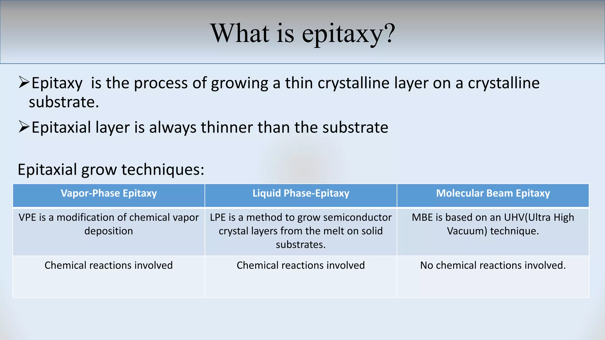
Definition of epitaxy, types including homoepitaxy and heteroepitaxy, and techniques used.
Exploration of the three main growth modes influenced by temperature, deposition rate, and energy.
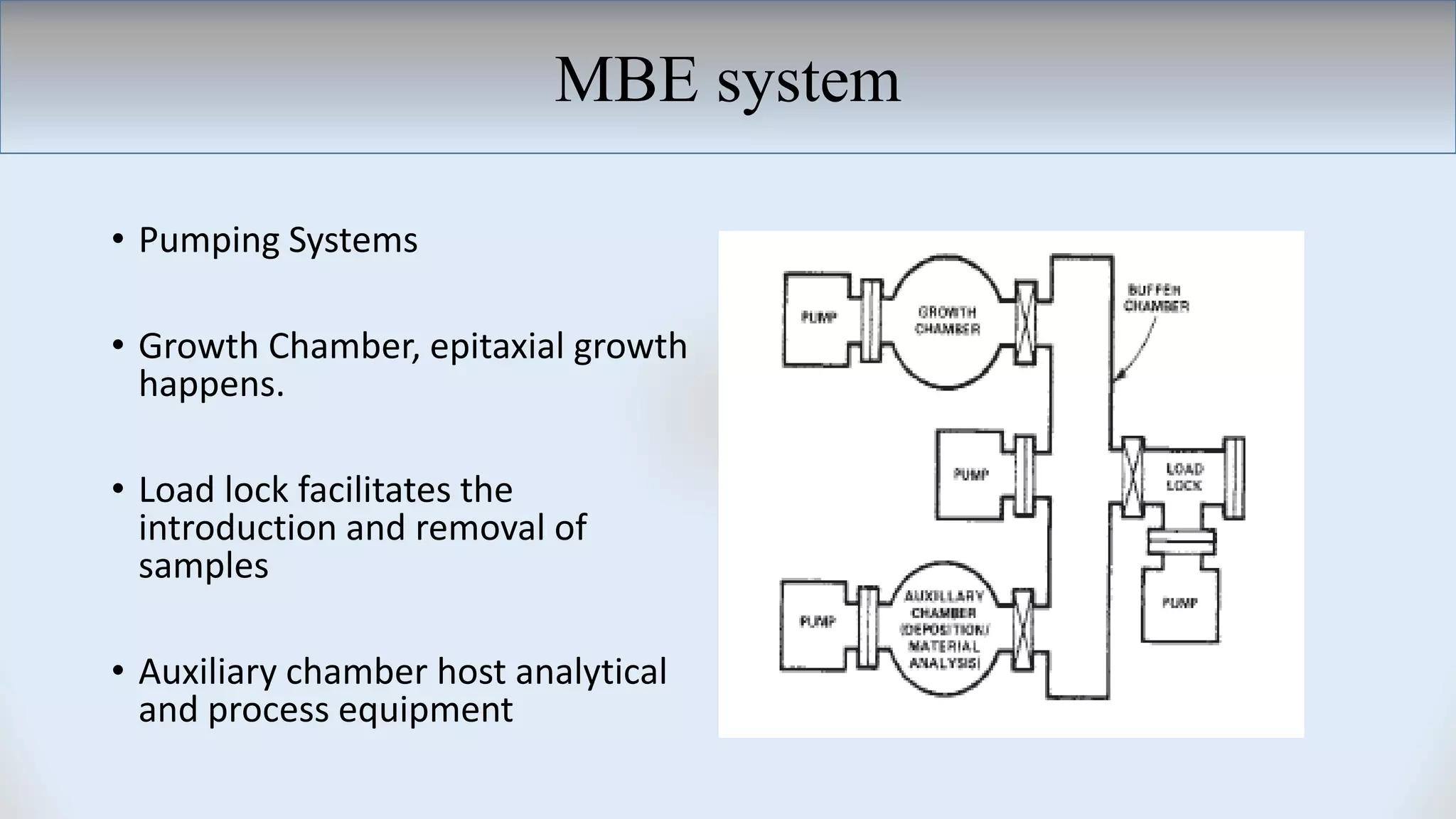
Detailed introduction to MBE, including its system components like the growth chamber and load lock.
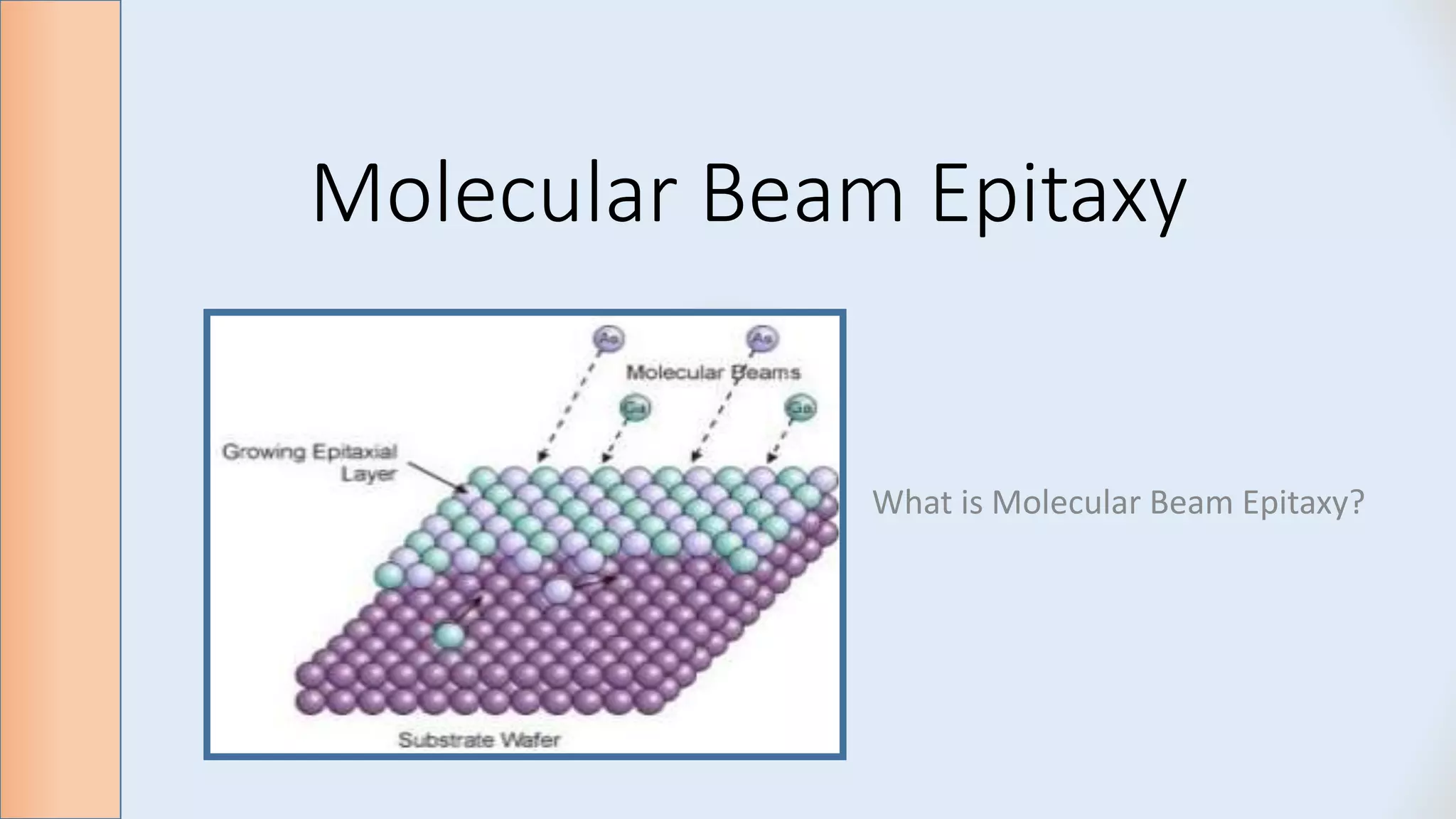
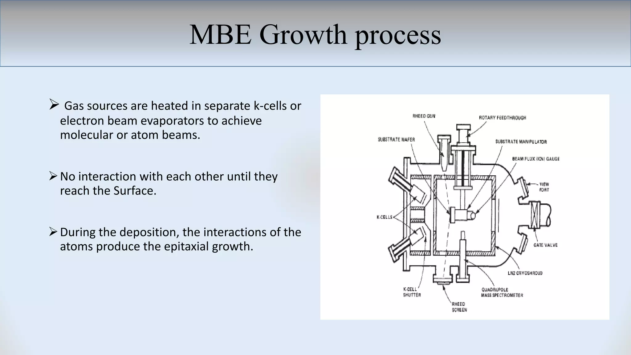
Process of producing molecular or atomic beams and their interaction leading to epitaxial growth.
Key features of MBE with specific numerical data on deposition rate, growth temperature, and thickness control.
Use of Reflection High Energy Electron Diffraction (RHEED) for monitoring growth, calibration, and analysis.
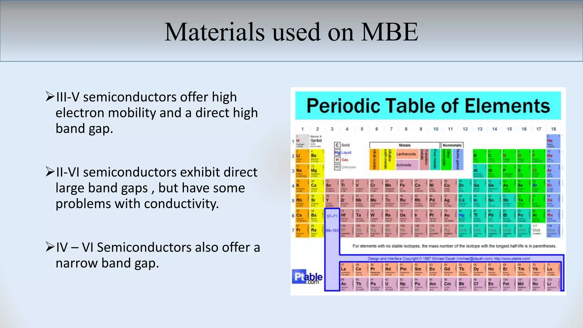
Focus on solid-source MBE with types of materials used, including III-V, II-VI, and IV-VI semiconductors.
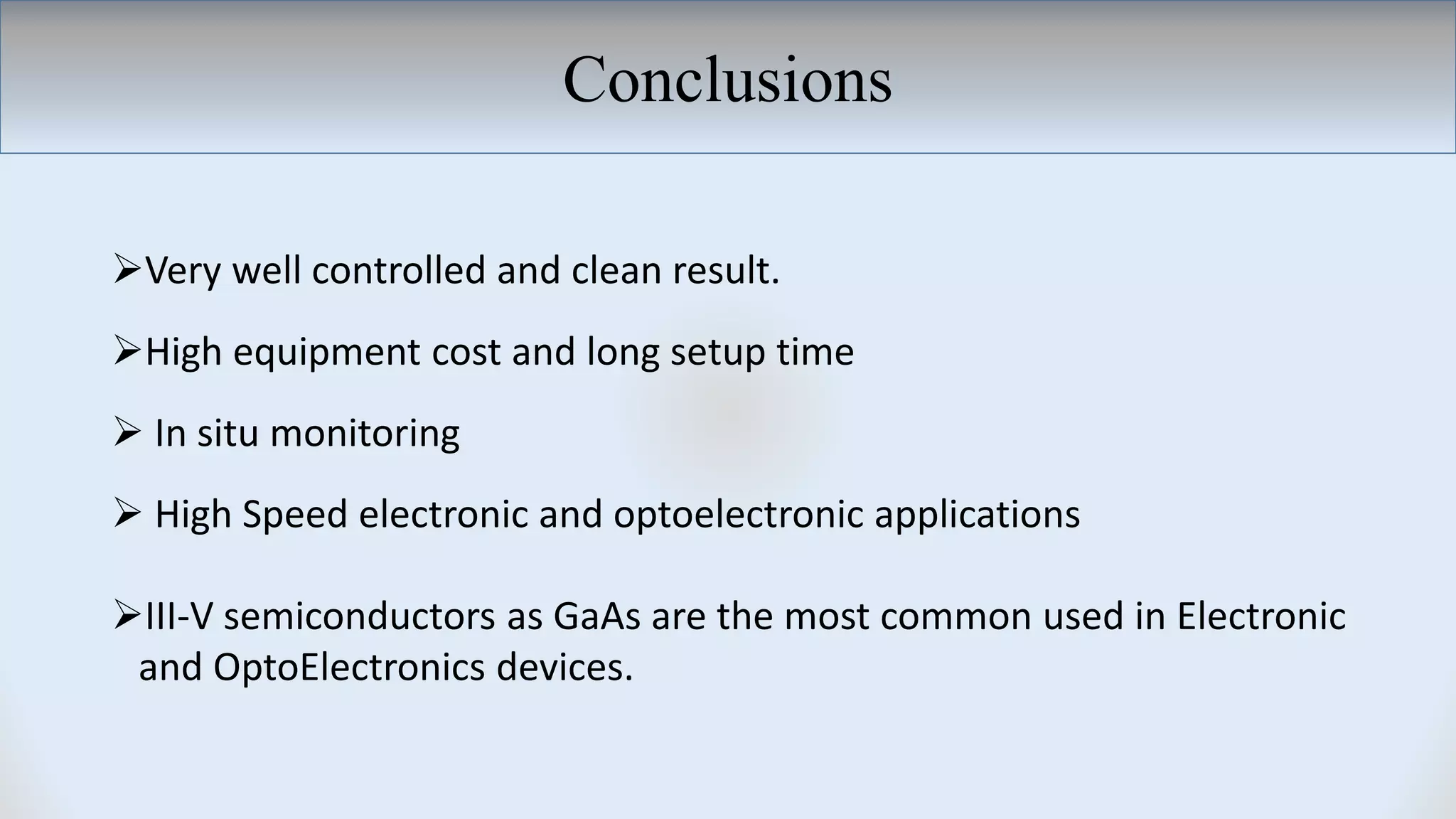
Advantages like clean surfaces and monitoring, alongside challenges like cost and flexibility issues.
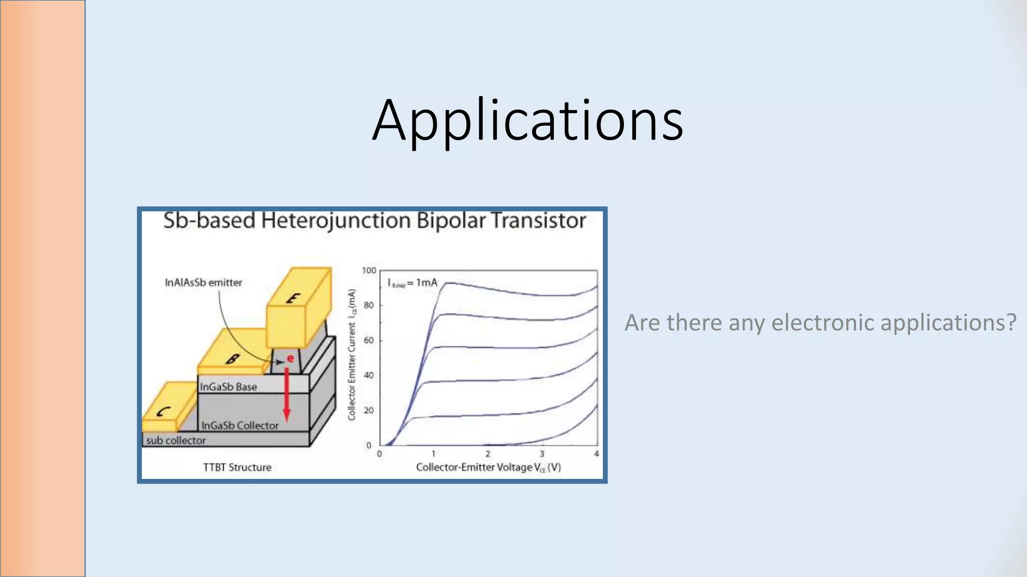
Current applications in advanced electronic and optoelectronic devices, including specific types.
Summary of MBE advantages, challenges, and its significance in high-speed applications.
Open floor for questions and clarifications on MBE and its applications.


![Thin_Film_Technology_introduction[1]](https://cdn.slidesharecdn.com/ss_thumbnails/1b4496c8-2102-411b-8465-a3dd3f398327-150205034538-conversion-gate02-thumbnail.jpg?width=640&height=640&fit=bounds)


