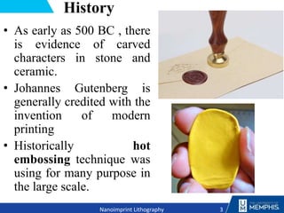
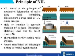
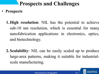
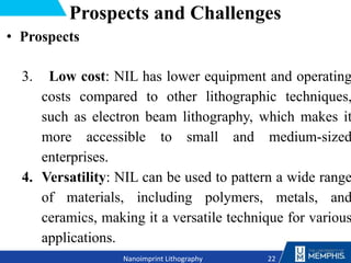
Nanoimprint Lithography
By
Debendra Timsina
Department of Physics and Material Science
University of Memphis
1
Nanoimprint Lithography
Outlines
History
Introduction
Types of NIL
Applications
Prospects and Challenges
Conclusion
2
Nanoimprint Lithography
History
• As early as 500 BC , there
is evidence of carved
characters in stone and
ceramic.
• Johannes Gutenberg is
generally credited with the
invention of modern
printing
• Historically hot
embossing technique was
using for many purpose in
the large scale.
3
Nanoimprint Lithography
Introduction
• Nanoimprint Lithography
(NIL) first used by Prof
Stephen Chou and his
students in scientific
community in 1996.
• NIL is simple cost-
effective, high throughput
and high-resolution
process.
• NIL able to get high
resolution feature size up
to 2 nm with high
throughput.
4
Nanoimprint Lithography
Principle of NIL
• NIL works on the principle of
mechanical deformation of resists
using mold containing
nanostructure during heat or UV
curing process.
• Mold or template is generally
prepared by E-beam lithography.
Materials used like Si, SiO2,
Quartz, Ni
• Thermoplastic or UV curable resist
are used.
• Pattern transferred by anisotropic
etching to remove residue resist.
5
Nanoimprint Lithography
Two Fundamentals Types of NIL
• Thermal NIL
– Step 1:Resist coating
• Stamp materials: Si, SiO2,
Opaque
• Resist: Thermoplastic Polymer
(PMMA)
• Viscosity: 103- 107 Pa S
– Step 2: Heat & Press
• Temperature:100-200°C > Tg
• Pressure:20-100 bar
– Step 3: Cool and Separate
• Demold T: 20-80 °C
• UV- NIL
– Step 1 : Resist Coating
• Stamp materials: Glass, SiO2
transparent.
• Resist: Liquid photopolymer
(SU-8)
• Viscosity: 10-2- 10-3 Pa S
– Step 2: Press & UV Expose
• Temperature: 20 °C (RT)
• Pressure 0-5 bar
– Step 3: Separate Demold T:
20 °C (RT)
6
Nanoimprint Lithography
Both thermal and UV-NIL have demonstrated a sub-10 nm resolution.
Other Types of NIL
• Hard UV-NIL
– Hard mold; quartz glass
– releasing agent required
– surface waviness limit
imprint area
– Difficult to insure uniform
and parallel surface
contact
• Soft UV-NIL
– Soft mild like PDMS
– No conglutination
– High pattern transferring
area
– High pression feature
– Reduce parallelism error
between mold and
substrate
– But resolution limitation
and non uniformity
7
Nanoimprint Lithography
Types of UV-NIL
8
Nanoimprint Lithography
Combination of UV and Thermal NIL
Thermal expansion
mismatch between
stamp and substrate
are avoided
Reverse NIL
 Spin-coated onto the mold rather than substrate
 Mold has low surface energy than substrate
 Able to construct 3-D and Multilayer micro/nano structure.
9
Nanoimprint Lithography
Jet and Flash Imprint Lithography
10
Nanoimprint Lithography
 Able to imprint in
large depressed
surface and thick
film
Laser Assisted NIL
11
Nanoimprint Lithography
• Used to make nano
structure in Si and metal.
• Rapid process
• Doesn’t required etching
• Resolution better than 10
nm
• Can be used for large
area pattern (a whole
wafer)
Roll Imprint Process (RNIL)
Advantages
• Continues process
• High Throughput
• Low cost
• Low energy
• Simple system
construction
12
Nanoimprint Lithography
Steps
• Deposition
• Patterning
• Packaging
13
Nanoimprint Lithography
RNIL: Mold Type
Two Method of RNIL
I. Roller Mold
II.Flat Mold and
smooth Roller
Two Substate Type
– Flexible
– Rigid
14
Nanoimprint Lithography
RNIL: Substrates Type
15
Nanoimprint Lithography
Nanoelectrode Lithography
Combine nanoimprint with
electrochemical reaction
The conductive mold
pattern undergoes an
electrochemical reaction
that enables an oxide
pattern to be fabricated
directly on the surface of a
semiconductor or metal
layer.
Resistless and multiple
patterning will improve
accuracy and flexibility
16
Nanoimprint Lithography
Dynamic Nanoscribing Lithography
• Creates continuous structures
over substrates of any length
• DNI can be applied to many
polymer films and the
resulting pattern profile can
be controlled by the localized
heating.
• DNI enables continuous
patterning on flat or curved
surfaces and can follow
circular or bent path as well
17
Nanoimprint Lithography
Dynamic
Nanoscribing
(DNI)
Laser Assisted
Direct Imprint
(LADI)
Nanoimprint
Lithography
Variant Based
on Resist curing
Unconventional Imprint
Roll-to-Roll
Conventional Imprint
Variant Based
on Mold Type
Variant Based
on Contact
Method
Thermal
UV
Plate-to-
Plate
Roll-to-Plate
Hard Mold
Imprint
Soft Mold Imprint
Functional
Resin
Imprint
Nanoelectrode
Lithography
(NEL)
Classifications of NIL
Application of NIL
• NIL technique used to make
– Memory devices: HDD, NAND flash memory
– Optical Storage Device :HD-DVD, Blue-Ray
– High Brightness LED, OLED, LCD, field emission
display, organic light emitting display
– Optical elements : Lens, diffractive grating, waveguide,
tunable optical filter, nano wire grid polarizer
– Biological devices: Biosensors, Biomedicine,
Nanofluidic devices, microarrays for genomics,
proteomics and tissue engineering, nanoscale protein
patterning
18
Nanoimprint Lithography
–Nanoelectronics: molecular electronics, AFM
tips
–High-end semiconductors and high-density
interconnects, other NEMS/MEMS
applications: solar cell, fuse cell, CNT sensor,
etc.
– Manufacturing of metasurfaces which has
application in optical communicating, sensing,
energy harvesting etc.
– 3-D printing, multi layer nano channels
19
Nanoimprint Lithography
Application of NIL
Applications of NIL
20
Nanoimprint Lithography
Prospects and Challenges
• Prospects
1.High resolution: NIL has the potential to achieve
sub-10 nm resolution, which is essential for many
nanofabrication applications in electronics, optics,
and biotechnology.
2.Scalability: NIL can be easily scaled up to produce
large-area patterns, making it suitable for industrial-
scale manufacturing.
21
Nanoimprint Lithography
Prospects and Challenges
• Prospects
3. Low cost: NIL has lower equipment and operating
costs compared to other lithographic techniques,
such as electron beam lithography, which makes it
more accessible to small and medium-sized
enterprises.
4. Versatility: NIL can be used to pattern a wide range
of materials, including polymers, metals, and
ceramics, making it a versatile technique for various
applications.
22
Nanoimprint Lithography
Prospects and Challenges
• Challenges
1. Template fabrication: The fabrication of high-quality
templates or molds with sub-10 nm resolution is challenging
and time-consuming. The cost of the templates can also be
high, especially for high-resolution patterns.
2. Material properties: The choice of resist material is critical
for achieving high-resolution patterns using NIL. However,
not all materials are suitable for NIL, and some may exhibit
unwanted properties, such as shrinkage or cracking.
3. Alignment: The alignment of the template with the substrate
is critical for achieving high-resolution patterns. However,
misalignment can occur, leading to defects in the pattern.
23
Nanoimprint Lithography
Prospects and Challenges
• Challenges
4. Large-area patterning: Although NIL can be easily scaled
up to produce large-area patterns, the uniformity and
consistency of the patterns can be challenging to achieve
over large areas.
5. Integration with other techniques: NIL may need to be
integrated with other lithographic techniques, such as
electron beam lithography or photolithography, to achieve
even higher resolution patterns or more complex device
structures. However, the integration of these techniques can
be challenging and may require additional processing steps
24
Nanoimprint Lithography
Conclusion
In conclusion, Nanoimprint lithography (NIL) is a promising nanofabrication
technique that can produce high-resolution patterns with low cost and high
throughput. Recent advances in NIL have further improved its performance
and capabilities, including the development of high-resolution templates,
advanced resist materials, soft imprint lithography, roll-to-roll NIL, and hybrid
imprint lithography.
However, NIL still faces several challenges, including template fabrication,
material properties, alignment, large-area patterning, and integration with other
lithographic techniques. Despite the challenges, the potential benefits of NIL
make it an exciting technology with many promising applications in
electronics, optics, and biotechnology.
25
Nanoimprint Lithography
References
1. Lan H, Ding Y. Nanoimprint Lithography. In: Lithography. InTech.
2. Resnick D. Nanoimprint lithography. In: Nanolithography: The Art of Fabricating Nanoelectronic and Nanophotonic Devices and Systems. Elsevier Ltd,
2013, p. 315–347.
3. Chou S. Nanoimprint lithography. Technol Rev 106: 42, 2003.
4. Chou SY, Krauss PR, Renstrom PJ. Imprint of sub-25 nm vias and trenches in polymers. Appl Phys Lett 67: 3114, 1995. doi: 10.1063/1.114851.
5. Hua F, Sun Y, Gaur A, Meitl MA, Bilhaut L, Rotkina L, Wang J, Geil P, Shim M, Rogers JA, Shim A. Polymer imprint lithography with molecular-
scale resolution. Nano Lett 4: 2467–2471, 2004. doi: 10.1021/nl048355u.
6. Handrea-Dragan M, Botiz I. Multifunctional structured platforms: From patterning of polymer-based films to their subsequent filling with various
nanomaterials. Polymers (Basel) 13 MDPI AG: 1–49, 2021
7. Higashiki T. Nanoimprint lithography and future patterning for semiconductor devices. Journal of Micro/Nanolithography, MEMS, and MOEMS 10:
043008, 2011. doi: 10.1117/1.3658024.
8. Nanoimprint Lithography – YouTube
9. Kehagias N, Reboud V, Chansin G, Zelsmann M, Jeppesen C, Reuther F, Schuster C, Kubenz M, Gruetzner G, Sotomayor Torres CM. Submicron
three-dimensional structures fabricated by reverse contact UV nanoimprint lithography. Journal of Vacuum Science & Technology B: Microelectronics and
Nanometer Structures 24: 3002, 2006. doi: 10.1116/1.2388962.
10. Colburn M, Grot A, Amistoso MN, Choi BJ, Bailey TC, Ekerdt JG, Sreenivasan S V., Hollenhorst J, Willson CG. Step and flash imprint lithography
for sub-100-nm patterning. In: Emerging Lithographic Technologies IV. SPIE, 2000, p. 453–457.
11. Han KS, Hong SH, Lee H. Fabrication of complex nanoscale structures on various substrates. Appl Phys Lett 91, 2007. doi: 10.1063/1.2789735.
12. Chou SY, Keimel C, Gu J. Ultrafast and direct imprint of nanostructures in silicon. Nature 417: 835–837, 2002. doi: 10.1038/nature00792.
13. Lee T, Lee C, Oh DK, Badloe T, Ok JG, Rho J. Scalable and high-throughput top-down manufacturing of optical metasurfaces. Sensors (Switzerland) 20
MDPI AG: 1–33, 2020.
14. Yokoo A, Namatsu H. NTT Technical Review [Online]. https://www.ntt-review.jp/archive/ntttechnical.php?contents=ntr200808sp3.pdf&mode=show_pdf
26
Nanoimprint Lithography
Thank You!
27
Nanoimprint Lithography

Nanoimprint Lithography

  • 1.
    Nanoimprint Lithography By Debendra Timsina Departmentof Physics and Material Science University of Memphis 1 Nanoimprint Lithography
  • 2.
    Outlines History Introduction Types of NIL Applications Prospectsand Challenges Conclusion 2 Nanoimprint Lithography
  • 3.
    History • As earlyas 500 BC , there is evidence of carved characters in stone and ceramic. • Johannes Gutenberg is generally credited with the invention of modern printing • Historically hot embossing technique was using for many purpose in the large scale. 3 Nanoimprint Lithography
  • 4.
    Introduction • Nanoimprint Lithography (NIL)first used by Prof Stephen Chou and his students in scientific community in 1996. • NIL is simple cost- effective, high throughput and high-resolution process. • NIL able to get high resolution feature size up to 2 nm with high throughput. 4 Nanoimprint Lithography
  • 5.
    Principle of NIL •NIL works on the principle of mechanical deformation of resists using mold containing nanostructure during heat or UV curing process. • Mold or template is generally prepared by E-beam lithography. Materials used like Si, SiO2, Quartz, Ni • Thermoplastic or UV curable resist are used. • Pattern transferred by anisotropic etching to remove residue resist. 5 Nanoimprint Lithography
  • 6.
    Two Fundamentals Typesof NIL • Thermal NIL – Step 1:Resist coating • Stamp materials: Si, SiO2, Opaque • Resist: Thermoplastic Polymer (PMMA) • Viscosity: 103- 107 Pa S – Step 2: Heat & Press • Temperature:100-200°C > Tg • Pressure:20-100 bar – Step 3: Cool and Separate • Demold T: 20-80 °C • UV- NIL – Step 1 : Resist Coating • Stamp materials: Glass, SiO2 transparent. • Resist: Liquid photopolymer (SU-8) • Viscosity: 10-2- 10-3 Pa S – Step 2: Press & UV Expose • Temperature: 20 °C (RT) • Pressure 0-5 bar – Step 3: Separate Demold T: 20 °C (RT) 6 Nanoimprint Lithography Both thermal and UV-NIL have demonstrated a sub-10 nm resolution.
  • 7.
    Other Types ofNIL • Hard UV-NIL – Hard mold; quartz glass – releasing agent required – surface waviness limit imprint area – Difficult to insure uniform and parallel surface contact • Soft UV-NIL – Soft mild like PDMS – No conglutination – High pattern transferring area – High pression feature – Reduce parallelism error between mold and substrate – But resolution limitation and non uniformity 7 Nanoimprint Lithography Types of UV-NIL
  • 8.
    8 Nanoimprint Lithography Combination ofUV and Thermal NIL Thermal expansion mismatch between stamp and substrate are avoided
  • 9.
    Reverse NIL  Spin-coatedonto the mold rather than substrate  Mold has low surface energy than substrate  Able to construct 3-D and Multilayer micro/nano structure. 9 Nanoimprint Lithography
  • 10.
    Jet and FlashImprint Lithography 10 Nanoimprint Lithography  Able to imprint in large depressed surface and thick film
  • 11.
    Laser Assisted NIL 11 NanoimprintLithography • Used to make nano structure in Si and metal. • Rapid process • Doesn’t required etching • Resolution better than 10 nm • Can be used for large area pattern (a whole wafer)
  • 12.
    Roll Imprint Process(RNIL) Advantages • Continues process • High Throughput • Low cost • Low energy • Simple system construction 12 Nanoimprint Lithography Steps • Deposition • Patterning • Packaging
  • 13.
    13 Nanoimprint Lithography RNIL: MoldType Two Method of RNIL I. Roller Mold II.Flat Mold and smooth Roller
  • 14.
    Two Substate Type –Flexible – Rigid 14 Nanoimprint Lithography RNIL: Substrates Type
  • 15.
    15 Nanoimprint Lithography Nanoelectrode Lithography Combinenanoimprint with electrochemical reaction The conductive mold pattern undergoes an electrochemical reaction that enables an oxide pattern to be fabricated directly on the surface of a semiconductor or metal layer. Resistless and multiple patterning will improve accuracy and flexibility
  • 16.
    16 Nanoimprint Lithography Dynamic NanoscribingLithography • Creates continuous structures over substrates of any length • DNI can be applied to many polymer films and the resulting pattern profile can be controlled by the localized heating. • DNI enables continuous patterning on flat or curved surfaces and can follow circular or bent path as well
  • 17.
    17 Nanoimprint Lithography Dynamic Nanoscribing (DNI) Laser Assisted DirectImprint (LADI) Nanoimprint Lithography Variant Based on Resist curing Unconventional Imprint Roll-to-Roll Conventional Imprint Variant Based on Mold Type Variant Based on Contact Method Thermal UV Plate-to- Plate Roll-to-Plate Hard Mold Imprint Soft Mold Imprint Functional Resin Imprint Nanoelectrode Lithography (NEL) Classifications of NIL
  • 18.
    Application of NIL •NIL technique used to make – Memory devices: HDD, NAND flash memory – Optical Storage Device :HD-DVD, Blue-Ray – High Brightness LED, OLED, LCD, field emission display, organic light emitting display – Optical elements : Lens, diffractive grating, waveguide, tunable optical filter, nano wire grid polarizer – Biological devices: Biosensors, Biomedicine, Nanofluidic devices, microarrays for genomics, proteomics and tissue engineering, nanoscale protein patterning 18 Nanoimprint Lithography
  • 19.
    –Nanoelectronics: molecular electronics,AFM tips –High-end semiconductors and high-density interconnects, other NEMS/MEMS applications: solar cell, fuse cell, CNT sensor, etc. – Manufacturing of metasurfaces which has application in optical communicating, sensing, energy harvesting etc. – 3-D printing, multi layer nano channels 19 Nanoimprint Lithography Application of NIL
  • 20.
  • 21.
    Prospects and Challenges •Prospects 1.High resolution: NIL has the potential to achieve sub-10 nm resolution, which is essential for many nanofabrication applications in electronics, optics, and biotechnology. 2.Scalability: NIL can be easily scaled up to produce large-area patterns, making it suitable for industrial- scale manufacturing. 21 Nanoimprint Lithography
  • 22.
    Prospects and Challenges •Prospects 3. Low cost: NIL has lower equipment and operating costs compared to other lithographic techniques, such as electron beam lithography, which makes it more accessible to small and medium-sized enterprises. 4. Versatility: NIL can be used to pattern a wide range of materials, including polymers, metals, and ceramics, making it a versatile technique for various applications. 22 Nanoimprint Lithography
  • 23.
    Prospects and Challenges •Challenges 1. Template fabrication: The fabrication of high-quality templates or molds with sub-10 nm resolution is challenging and time-consuming. The cost of the templates can also be high, especially for high-resolution patterns. 2. Material properties: The choice of resist material is critical for achieving high-resolution patterns using NIL. However, not all materials are suitable for NIL, and some may exhibit unwanted properties, such as shrinkage or cracking. 3. Alignment: The alignment of the template with the substrate is critical for achieving high-resolution patterns. However, misalignment can occur, leading to defects in the pattern. 23 Nanoimprint Lithography
  • 24.
    Prospects and Challenges •Challenges 4. Large-area patterning: Although NIL can be easily scaled up to produce large-area patterns, the uniformity and consistency of the patterns can be challenging to achieve over large areas. 5. Integration with other techniques: NIL may need to be integrated with other lithographic techniques, such as electron beam lithography or photolithography, to achieve even higher resolution patterns or more complex device structures. However, the integration of these techniques can be challenging and may require additional processing steps 24 Nanoimprint Lithography
  • 25.
    Conclusion In conclusion, Nanoimprintlithography (NIL) is a promising nanofabrication technique that can produce high-resolution patterns with low cost and high throughput. Recent advances in NIL have further improved its performance and capabilities, including the development of high-resolution templates, advanced resist materials, soft imprint lithography, roll-to-roll NIL, and hybrid imprint lithography. However, NIL still faces several challenges, including template fabrication, material properties, alignment, large-area patterning, and integration with other lithographic techniques. Despite the challenges, the potential benefits of NIL make it an exciting technology with many promising applications in electronics, optics, and biotechnology. 25 Nanoimprint Lithography
  • 26.
    References 1. Lan H,Ding Y. Nanoimprint Lithography. In: Lithography. InTech. 2. Resnick D. Nanoimprint lithography. In: Nanolithography: The Art of Fabricating Nanoelectronic and Nanophotonic Devices and Systems. Elsevier Ltd, 2013, p. 315–347. 3. Chou S. Nanoimprint lithography. Technol Rev 106: 42, 2003. 4. Chou SY, Krauss PR, Renstrom PJ. Imprint of sub-25 nm vias and trenches in polymers. Appl Phys Lett 67: 3114, 1995. doi: 10.1063/1.114851. 5. Hua F, Sun Y, Gaur A, Meitl MA, Bilhaut L, Rotkina L, Wang J, Geil P, Shim M, Rogers JA, Shim A. Polymer imprint lithography with molecular- scale resolution. Nano Lett 4: 2467–2471, 2004. doi: 10.1021/nl048355u. 6. Handrea-Dragan M, Botiz I. Multifunctional structured platforms: From patterning of polymer-based films to their subsequent filling with various nanomaterials. Polymers (Basel) 13 MDPI AG: 1–49, 2021 7. Higashiki T. Nanoimprint lithography and future patterning for semiconductor devices. Journal of Micro/Nanolithography, MEMS, and MOEMS 10: 043008, 2011. doi: 10.1117/1.3658024. 8. Nanoimprint Lithography – YouTube 9. Kehagias N, Reboud V, Chansin G, Zelsmann M, Jeppesen C, Reuther F, Schuster C, Kubenz M, Gruetzner G, Sotomayor Torres CM. Submicron three-dimensional structures fabricated by reverse contact UV nanoimprint lithography. Journal of Vacuum Science & Technology B: Microelectronics and Nanometer Structures 24: 3002, 2006. doi: 10.1116/1.2388962. 10. Colburn M, Grot A, Amistoso MN, Choi BJ, Bailey TC, Ekerdt JG, Sreenivasan S V., Hollenhorst J, Willson CG. Step and flash imprint lithography for sub-100-nm patterning. In: Emerging Lithographic Technologies IV. SPIE, 2000, p. 453–457. 11. Han KS, Hong SH, Lee H. Fabrication of complex nanoscale structures on various substrates. Appl Phys Lett 91, 2007. doi: 10.1063/1.2789735. 12. Chou SY, Keimel C, Gu J. Ultrafast and direct imprint of nanostructures in silicon. Nature 417: 835–837, 2002. doi: 10.1038/nature00792. 13. Lee T, Lee C, Oh DK, Badloe T, Ok JG, Rho J. Scalable and high-throughput top-down manufacturing of optical metasurfaces. Sensors (Switzerland) 20 MDPI AG: 1–33, 2020. 14. Yokoo A, Namatsu H. NTT Technical Review [Online]. https://www.ntt-review.jp/archive/ntttechnical.php?contents=ntr200808sp3.pdf&mode=show_pdf 26 Nanoimprint Lithography
  • 27.