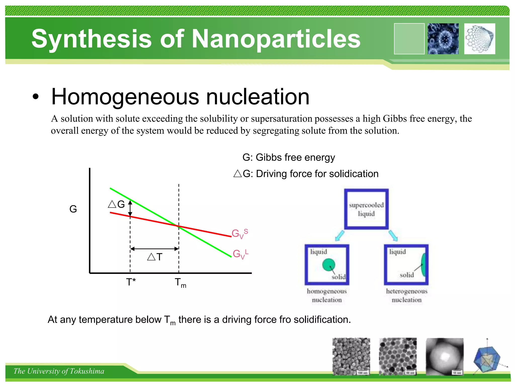
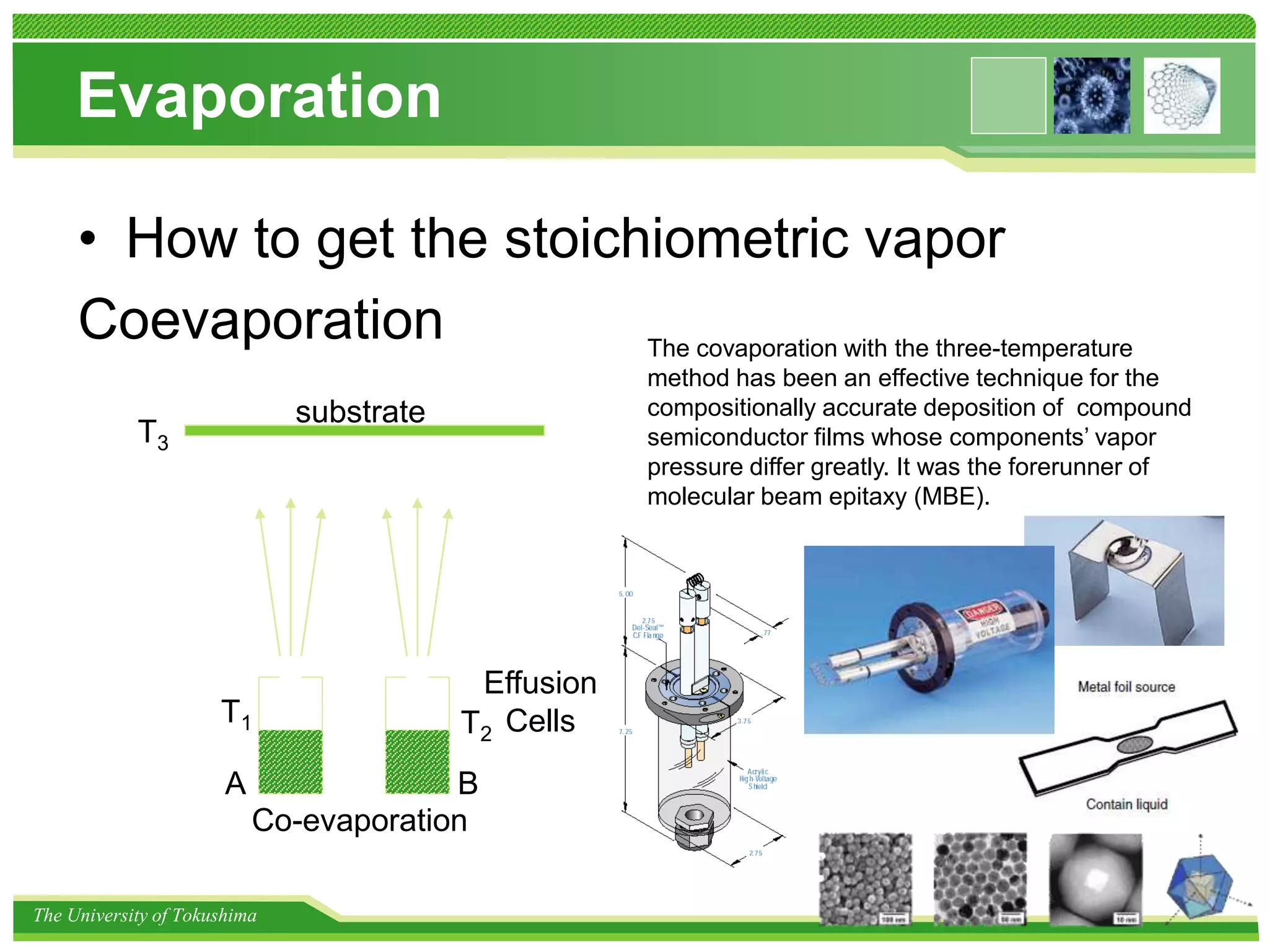
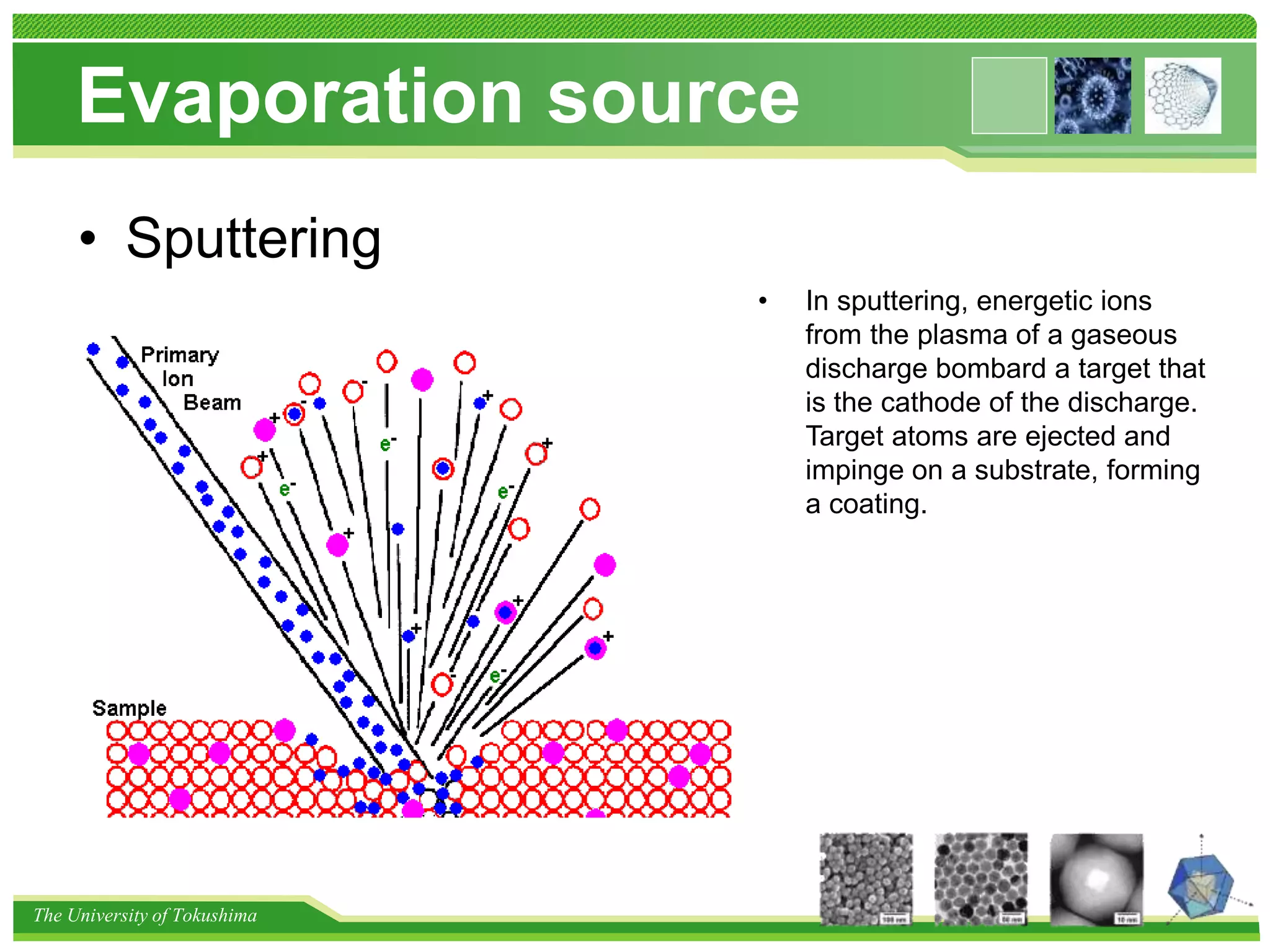
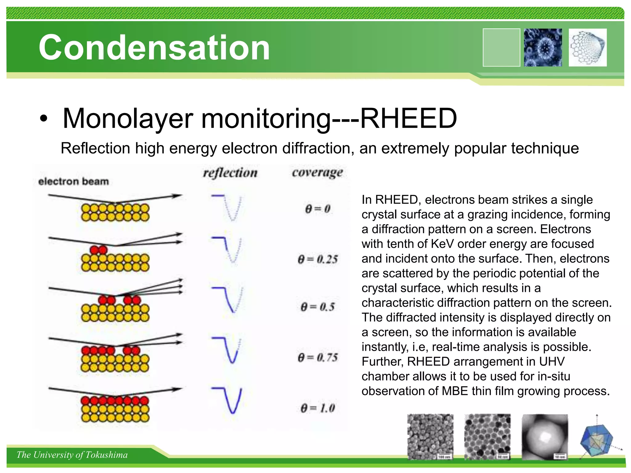
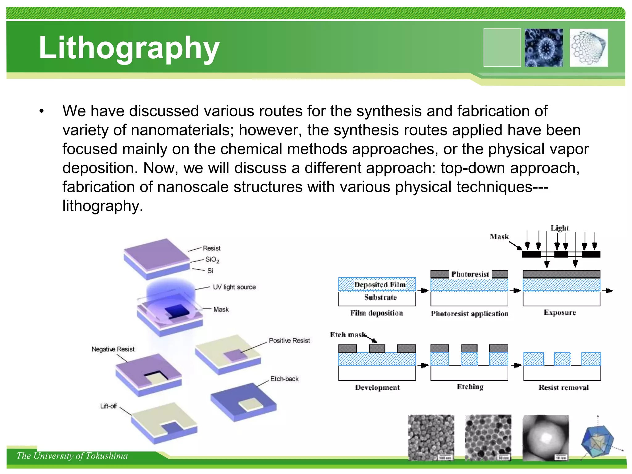
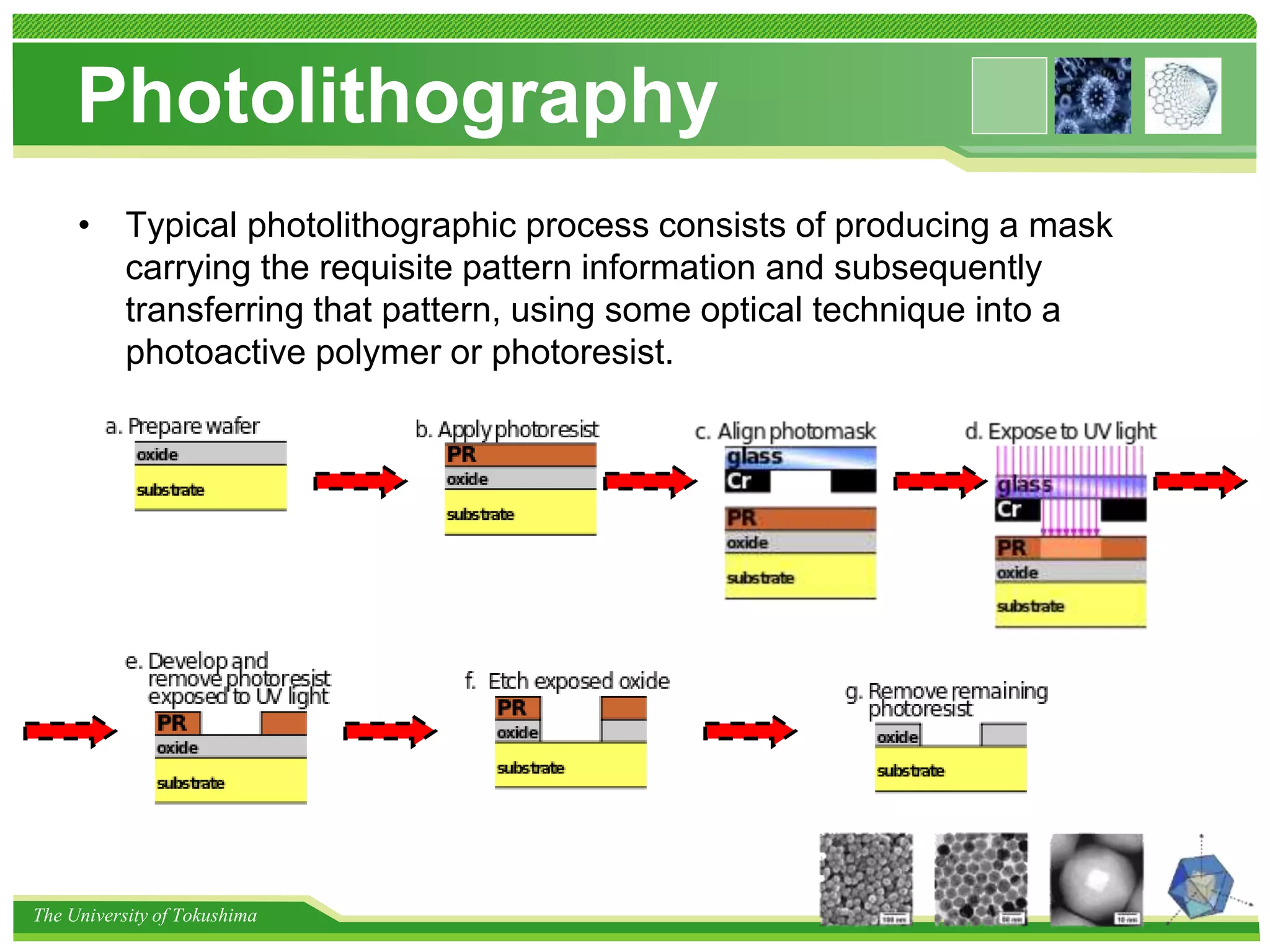
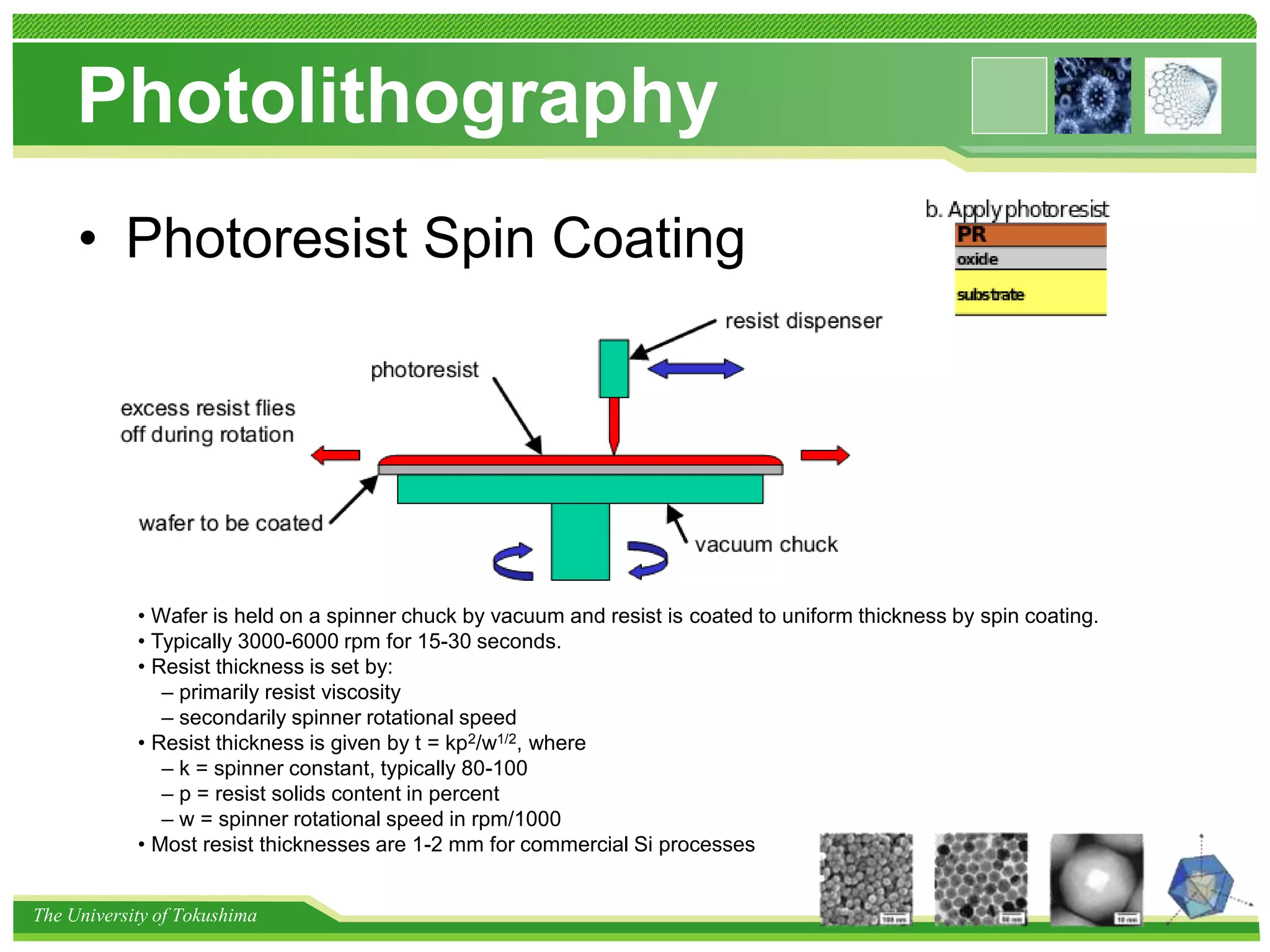
Nanomaterial Synthesis Method
Nanoscience and nanotechnology
Ri-ichi Murakami
The University of Tokushima
Nanomaterial Synthesis Method
There's Plenty of Room at the Bottom
By Richard Feyman in 1959
Nanotechnology application in nowadays
Targeted drug delivery
Super nano-capacitors
CNT Transistor
The University of Tokushima
Outline
Emergence and Challenges in Nanotechnology
Bottom-Up and Top-Down Approaches
Introduction to synthesis of nanoparticles
Evaporation and Condensation growth
Lithography technology
Method to nano composite structure
The University of Tokushima
Emergence of Nano
• Moore’s Law
Moore’s Law plot of transistor size versus year
Original contact transistor
1947
~cm
Transistor
in Integrated circuit
Nowadays
~micrometer
CNT Transistor
Future
~nanometer
To meet the Moore’s Law, the size of transistor should be decreased
The University of Tokushima
Emergence of Nano
• In our life
1. LED for display
2. PV film
3. Self-cleaning window
4. Temperature control fabrics
5. Health Monitoring clothes
6. CNT chair
7. Biocompatible materials
8. Nano-particle paint
9. Smart window
10. Data memory
11. CNT fuel cells
12. Nano-engineered cochlear
The nanotechnology is changing our life, but not enough.
Energy crisis, environmental problem, health monitoring, Artifical joints
The University of Tokushima
Challenges in Nano
• Atomic scale imaging
Understand and manipulate the target in nano scale
LaSrMnO and SrTiO superlattice
TEM in biology
The University of Tokushima
Challenges in Nano
• Interdisciplinary Investigation
Nano drug delivery
Protein TEM image
Nano mechanics
Biology
&
Medicine
Physics
&
Chemistry
&
Materials
Mechanics
&
Electronics
Nano
The University of Tokushima
Emergence and Challenges in Nanotechnology
Approaches
Introduction to synthesis of nanoparticles
Evaporation and Condensation growth
Lithography technology
Method to nano composite structure
Bottom-Up and Top-Down Approaches
The University of Tokushima
Approaches
• Obviously there are two approaches to the
synthesis of nanomaterials and the
fabrication of nanostructures:
• Top-down
• Bottom-up
Lithography
Self-assembly
The University of Tokushima
Emergence and Challenges in Nanotechnology
Synthesis of Nanoparticles
Introduction to synthesis of nanoparticles
Evaporation and Condensation growth
Lithography technology
Method to nano composite structure
Bottom-Up and Top-Down Approaches
The University of Tokushima
Synthesis of Nanoparticles
• Homogeneous nucleation
A solution with solute exceeding the solubility or supersaturation possesses a high Gibbs free energy, the
overall energy of the system would be reduced by segregating solute from the solution.
G △G
△T
GV
S
GV
L
TmT*
At any temperature below Tm there is a driving force fro solidification.
G: Gibbs free energy
△G: Driving force for solidication
The University of Tokushima
Synthesis of Nanoparticles
• Homogeneous nucleation
For nucleus with a radius r > r*, the Gibbs free
energy will decrease if the nucleus grow. r* is
the critical nucleus size, △G* is the nucleation
barrier.
The University of Tokushima
Synthesis of Nanoparticles
• Synthesis of metallic nanoparticles
Influences factors
Differenct reagents
A:sodium citrate
B: citric acid
A B
A weak reduction reagent
induces a slow reaction rate
and favors relatively larger
particles.
Concentration
A: 0.25M AgNO3
B: 0.125M AgNO3
A B
A large precursor
concentration induces a large
critical radius and favors
relarively larger particles.
Other factors: the surfactants, polymer stabilizer, temperature, ect
The details about the synthesis of nanoparticles via chemical
method would be introduced by other professors in this lecture.
The University of Tokushima
Emergence and Challenges in Nanotechnology
Evaporation and Condensation
Introduction to synthesis of nanoparticles
Evaporation and Condensation growth
Lithography technology
Method to nano composite structure
Bottom-Up and Top-Down Approaches
The University of Tokushima
Evaporation and Condensation
• The evaporation and condensation are the fundamental
phenomena in preparing thin films with nano meters
thickness.
Substrate
Condensation
Source
vapor
energy
Evaporation
If a condensible vapor is produced by physical
means and subsequently deposited on a solid
substrate, it is called physical vapor deposition.
If a volatile compound of a material react, with or
without other gases, to produce a nonvolatile solid
film, it is called the chemical vapor deposition.
Although both are nonequilibrium processes, the
kinetics and transport phenomena are the
fundamental theory.
The University of Tokushima
Evaporation and Condensation
• The Kinetic theoryLet’ s start with the equilibrium process.
Adsorption
Condensation
Substrate
The impingement rate:
the number of collisions per unit area per
second that a gas makes with a surface,
such as a chamber wall or a substrate
Supersaturation condition:
P, the gas pressure;m, the particle mass; k, Boltzmann’s constant, 1.38×10⁻²³ J/K; T, the temperature
ji, incident flux
Tsub, temperature of substrate
The substrate should be placed at relactively low temperature to meet the supersaturation condition.
The impingement rate indicates the equilibrium process between evaporation and condensation.
The University of Tokushima
Evaporation and Condensation
• The vapor source
The vapor is usually produced from a effusion cell, rather than a open system, therefore, we can solve the flow
density from the implingement rate.
zAJ 
Tsource Peq
J: flow density
A: area of the leak
z: implingement rate
On a certain angle cos
4
avn v
J

 
Source
substrate
The angle distribution is
important for a co-sputtering
condition.
Co-sputtering
The University of Tokushima
Evaporation and Condensation
• The vapor source
If we use a beer can as source material, what vapor will we obtain? Al 97.7%
Mg 1%
Mn 1.3%Consider the the implingement rate
beer can
Diffusion cell at 900 K
Mn atom
Al atom
Mg atom
Alloy source
Al, Mg, Mn have different atomic mass.Al: 0.0001%
Mn: 0.01%
Mg:99.99%
It is not practical to use a congruent
evaporation temperature to deposit a
compound (or alloy) film from a compound
(or alloy ) film with a certain stoichiometric.
This result is obtained under consideringt the adsorption and desorption effect.
The University of Tokushima
Evaporation
• How to get the stoichiometric vapor
Flash Evaporation
AC
Heater
substrate
Flash Evaporation
Flash evaporation utilizes very
rapid vaporization, typically by
dropping powders or grains of
the source material onto a hot
surface. The vapor condenses
rapidly onto a relatively cold
substrate, usually with the
same gross composition as
that of the source material.
The substrate was placed at a temperature
that was a supersaturation temperature for
each component.
The University of Tokushima
Evaporation
• How to get the stoichiometric vapor
E-Gun
AC
substrate
Molten End
E-Gun
Rod-Fed Source
e-
In a rod-fed source, typically an electron-beam-heated
evaporator, the source material evaporators from the
molten end of the rod. The rod advances as material is
lost from the molten end. In steady state, the
composition of the vapor stream must equal that of the
rod. This requires that the molten end be enriched in
the less volatile component. The adjustment is
automatic, since diffusion in the liquid state is rapid.
The University of Tokushima
Evaporation
• How to get the stoichiometric vapor
Coevaporation
substrate
A B
Effusion
Cells
Co-evaporation
T1 T2
T3
The covaporation with the three-temperature
method has been an effective technique for the
compositionally accurate deposition of compound
semiconductor films whose components’ vapor
pressure differ greatly. It was the forerunner of
molecular beam epitaxy (MBE).
The University of Tokushima
Evaporation
• How to get the stoichiometric vapor
Sputtering
Sputtering of certain materials, whose ejected particles are
molecules, was utilized to obtain a stoichiometric vapor.
•Direct current sputtering
•Direct current reactive sputtering
•Radio-frequency sputtering
The University of Tokushima
Evaporation
• The evaporation source
The simplest sources to produce vapors of materials may be thermal sources. These are sources
where thermal energy is utilized to produce the vapor of the evaporant material. Even when the
energy that is supplied to the evaporant may come from electrons or photons, the vaporizing
mechanism may still be thermal in nature.
quasiequilibrium
nonequilibrium
Evaporation
Sources
Effusion cell
Effusion cell
The University of Tokushima
Evaporation source
• Ideal Effusion Cell
δA
aorifice
L
Liquid
Gas, Peq
Lbody
1. The liquid and vapor are in equilibrium within
the cell. Pliq=Pvap, Tliq=Tvap, Gliq=Gvap
2. The mean free path inside the cell is much
greater than the orifice diameter.λ>>aorifice
3. The orifice is flat.
4. The orifice diameter is much less than the
distance to the receiving surface.
5. The wall thickness is much less than the
orifice diameter. L<<aorifice
How to design a effusion cell
The University of Tokushima
Evaporation source
• Near-ideal Effusion cell
It is impossible to design an ideal effusion cell
Direct
Re-emitted
L
Liquid
Gas, Peq
Lbody Lbody
With a thick orifice lid,
diffuse and specular
reflection off the
sidewalls are possible.
It is the restriction due to the long
cell body that cause a
nonequilibrium behavior of vapor.
The University of Tokushima
Evaporation source
• Open-Tube Effusion Cell
Figure 2.56
a
A quasiequilibrium source An open-tube effusion cell
L
The relative beam intensity
of the open-tube effusion cell
calculated for various tube
length-to-tube radius ratios
(L/a)
The University of Tokushima
Evaporation source
• E-Gun
A target anode is bombarded
with an electron beam given
off by a charged tungsten
filament under high vacuum.
The electron beam causes
atoms from the target to
transform into the gaseous
phase. These atoms then
precipitate into solid form,
coating everything in the
vacuum chamber (within line
of sight) with a thin layer of
the anode material.
The University of Tokushima
Evaporation source
• Pulsed Laser Deposition
A high power pulsed laser beam is
focused inside a vacuum chamber
to strike a target of the material
that is to be deposited. This
material is vaporized from the
target (in a plasma plume) which
deposits it as a thin film on a
substrate.
The University of Tokushima
Evaporation source
• Sputtering
• In sputtering, energetic ions
from the plasma of a gaseous
discharge bombard a target that
is the cathode of the discharge.
Target atoms are ejected and
impinge on a substrate, forming
a coating.
The University of Tokushima
Evaporation source
• Plasma-enhanced chemical vapor deposition
Plasma-enhanced chemical vapor depostion is a process used to deposit thin films from a gas state
(vapor) to a solid state on a substrate. Chemical reactions are involved in the process, which occur
after creation of a plasma of the reacting gases. The plasma is generally created by RF (AC)
frequency or DC discharge between twoelectrodes, the space between which is filled with the
reacting gases. A plasma is any gas in which a significant percentage of the atoms or molecules are
ionized. Fractional ionization in plasmas used for deposition and related materials processing varies
from about 10−4 in typical capacitive discharges to as high as 5–10% in high density inductive
plasmas.
The University of Tokushima
Condensation
• Condendation is the change of the physical state of matter from gaseous phase into
liquid phase or solid phase, and the reverse is vaporization.
condensation re-evaporation
adsorption
at special sit
surface
diffusion
nucleation
Inter diffusion
film growth
Adsorption of atoms from gaseous phase
Cluster formation
Critical size islands growth
Coalescence of neighboring islands
Percolation of islands network
Continuous film growth
film
The University of Tokushima
Condensation
• Adsorption
physisorption
chemisorption
gas
substrate
Van der Waals force
chemical bond
re-evaporationtransition
It is defined as chemisorption
coefficient that he fraction of
adsorbated atoms transferred from
physisorption into chemisorption but
not re-evaporated.
An critical condition is that the
adsorption is equall to the
reevaporation.
Only the atoms adsorpted on
the substrate and condensed,
grow bigger the critical radius,
then the film would be deposited.
The University of Tokushima
Condensation
• Condensation coefficient
substrate
incident flux
re-evaporation
condensation
The fraction of the incident
flux that actually condenses
c c ij a j
ji: the incident flux density
ac: the condensation coefficient
jc: the condensation flux
The University of Tokushima
Condensation
• Deposition Rate
Growth speed
a
5.430A
Si
cubic lattice parameter, 5.430 A
8 atoms per conventional unit cell
The volume per unit cell, (5.430 A)3=160.10 A3
The particle density, 8/(160.10 A3)=0.05 A-3
The growth speed
2
3
0.703 /
14.06 /
0.05
c
n
f
j A s
v s
n A


   
o
c
n
f
j
v
n

The deposition rate, or the growth speed
jc, the condensation flux
nf, the particle density,
how many particles per volume
An example
The University of Tokushima
Condensation
• Growth mode
The University of Tokushima
Condensation
• Non-epitaxial growth
For most film-substrate material combinations, film grow in the Volmer-
Weber (VW) mode which leads to a polycrystalline microstructure.
The University of Tokushima
Condensation
• Epitaxial growth---molecular beam epitaxy
Molecular beam epitaxy is a technique for epitaxial growth via the interaction
of one or several molecular or atomic beams that occurs on a surface of a
heated crystalline substrate.
The University of Tokushima
Condensation
• Epitaxial growth-Atomic layer deposition
based on the sequential use of a gas phase chemical process.
The University of Tokushima
Condensation
• Monolayer monitoring---RHEED
Reflection high energy electron diffraction, an extremely popular technique
for monitoring the growth of thin films.
In RHEED, electrons beam strikes a single
crystal surface at a grazing incidence, forming
a diffraction pattern on a screen. Electrons
with tenth of KeV order energy are focused
and incident onto the surface. Then, electrons
are scattered by the periodic potential of the
crystal surface, which results in a
characteristic diffraction pattern on the screen.
The diffracted intensity is displayed directly on
a screen, so the information is available
instantly, i.e, real-time analysis is possible.
Further, RHEED arrangement in UHV
chamber allows it to be used for in-situ
observation of MBE thin film growing process.
The University of Tokushima
Methods for deposition
Method ALD MBE CVD Sputtering Evapor PLD
Thickness Uniformity good fair good good fair fair
Film Density good good good good fair good
Step Coverage good poor varies poor poor poor
Interface Quality good good varies poor good varies
Low Temp. Depostion good good varies good good Good
Deposition Rate fair fair good good good Good
Industrial Application varies varies good good good poor
The University of Tokushima
Emergence and Challenges in Nanotechnology
Lithography
Introduction to synthesis of nanoparticles
Evaporation and Condensation growth
Lithography technology
Method to nano composite structure
Bottom-Up and Top-Down Approaches
The University of Tokushima
Lithography
• We have discussed various routes for the synthesis and fabrication of
variety of nanomaterials; however, the synthesis routes applied have been
focused mainly on the chemical methods approaches, or the physical vapor
deposition. Now, we will discuss a different approach: top-down approach,
fabrication of nanoscale structures with various physical techniques---
lithography.
The University of Tokushima
Lithography
Lithographic techniques
(a)Photolithography
(b)Phase shifting opitcal lithography
(c)Electron beam lithography
(e)Focused ion beam lithography
(f) Neutral atomic beam lithography
Nanomanipulation and nanolithography
(a)Scanning tunneling microscopy
(b)Atomic force microscopy
(c)Near-field scnning optical microscopy
(d)Nanomanipulation
(e)Nanolithography
The University of Tokushima
Photolithography
• Typical photolithographic process consists of producing a mask
carrying the requisite pattern information and subsequently
transferring that pattern, using some optical technique into a
photoactive polymer or photoresist.
The University of Tokushima
Photolithography
• Wafer preparation---cleaning
Typical contaminants that must be removed prior to photoresist coating:
•dust from scribing or cleaving (minimized by laser scribing)
•atmospheric dust (minimized by good clean room practice)
•abrasive particles (from lapping or CMP)
•lint from wipers (minimized by using lint-free wipers)
•photoresist residue from previous photolithography (minimized byperforming oxygen plasma ashing)
•bacteria (minimized by good DI water system)
•films from other sources:
–solvent residue
–H2O residue
–photoresist or developer residue
–oil
–silicone
Standard degrease:
– 2-5 min. soak in acetone with ultrasonic agitation
– 2-5 min. soak in methanol with ultrasonic agitation
– 2-5 min. soak in DI H2O with ultrasonic agitation
– 30 sec. rinse under free flowing DI H2O
– spin rinse dry for wafers; N2 blow off dry for tools and chucks
• For particularly troublesome grease, oil, or wax stains:
– Start with 2-5 min. soak in 1,1,1-trichloroethane (TCA) or trichloroethylene (TCE) with ultrasonic agitation prior to acetone
The University of Tokushima
Photolithography
• Wafer preparation---primers
 Adhesion promoters are used to assist resist coating.
 Resist adhesion factors:
•moisture content on surface
•wetting characteristics of resist
•type of primer
•delay in exposure and prebake
•resist chemistry
•surface smoothness
•stress from coating process
•surface contamination
Ideally want no H2O on wafer surface
– Wafers are given a “singe” step prior to priming and coating
•15 minutes in 80-90°C convection oven
Used for silicon:
– primers form bonds with surface and produce a polar (electrostatic) surface
– most are based upon siloxane linkages (Si-O-Si)
•1,1,1,3,3,3-hexamethyldisilazane (HMDS), (CH3)3SiNHSi(CH3)3
•trichlorophenylsilane (TCPS), C6H5SiCl3
•bistrimethylsilylacetamide (BSA), (CH3)3SiNCH3COSi(CH3)3
The University of Tokushima
Photolithography
• Photoresist Spin Coating
• Wafer is held on a spinner chuck by vacuum and resist is coated to uniform thickness by spin coating.
• Typically 3000-6000 rpm for 15-30 seconds.
• Resist thickness is set by:
– primarily resist viscosity
– secondarily spinner rotational speed
• Resist thickness is given by t = kp2/w1/2, where
– k = spinner constant, typically 80-100
– p = resist solids content in percent
– w = spinner rotational speed in rpm/1000
• Most resist thicknesses are 1-2 mm for commercial Si processes
The University of Tokushima
Photolithography
• Prebake
Used to evaporate the coating solvent and to densify the resist after spin coating.
• Typical thermal cycles:
– 90-100°C for 20 min. in a convection oven
– 75-85°C for 45 sec. on a hot plate
• Commercially, microwave heating or IR lamps are also used in production lines.
• Hot plating the resist is usually faster, more controllable, and does not trap solvent like convection oven baking.
The University of Tokushima
Photolithography
• Align/Expose/Develop
The University of Tokushima
Photolithography
• Etching/remove photoresist
photoresist has same polarity as final film;
photoresist never touches the substrate wafer.
The University of Tokushima
Photolithography
• Etching/remove photoresist
photoresist has opposite polarity as final film; excess
deposited film never touches the substrate wafer.
The University of Tokushima
Phase-shifting Photolithography
• Photolithography has a resolution limit. In order to
improve the resolution in photolithography, the phase-
shifting method was developed.
The University of Tokushima
E-beam lithography
• The theoretical resolution of photolithography is
)
2
(32 min
d
sb  
 The wavelength of the exposing radiation
s The gap width maintained between the masi and the photoresist surface
d The photoresist thickness
The wavelenght of electron beam is much smaller than UV light,
electron beams can be focused to a few nanometers in diameter and
can be deflected accurately and precisely over a surface.
The University of Tokushima
E-beam lithography
• Resist film
 Negative resist: After development, the
exposed structure is higher than the surrounding due
to crosslinking of polymer chains.
 Positive resist: After development, the exposed
structure is deeper than the surrounding due to
chopping of polymer chains.
 PMMA (Poly-methyle-metacrylate)
-one of the first e-beam resists (1968)
-standard positive resist
-resolution<10 nm
-medium sensitivity (150-300μC/cm2 )
-available with high (950K) and low (50k) molecular weight
-contrast: high for 950k-resist, low for 50k-resist
The University of Tokushima
E-beam lithography
• Challenge
 Charging effect: Complicate exact focusing
ofelectron-beam, displacement and distortion of
exposed structures.
 Proximity effect: Scattering of electrons in
resist film and substrate, unwanted additional
exposure.
The University of Tokushima
Focused ion beam lithography
• Advantages
-Ions have heavy mass than electrons.
-Less proximity effect than E-beam
-Less scattering effect
-High resolution patterning than UV, E-beam lithography
-Even smaller wavelength than E-beam
The University of Tokushima
Neutral atomic beam lithography
• In neutral atomic beams, no space charge effects make the beam divergent;
therefore, high kinetic particle energies are not required. Diffraction is no severe limit
for the resolution because the de Broglie wavelength of thermal atoms is less than 1
angstrom.
The University of Tokushima
Nanomanipulation and nanolithography
(a)Scanning tunneling microscopy
(b)Atomic force microscopy
(c)Near-field scnning optical microscopy
(d)Nanomanipulation
(e)Nanolithography
Nanomanipulation and
nanolithography are
based on scanning probe
microscopy.
The University of Tokushima
Scanning tunneling microscopy
• STM relies on electron tunneling, which is a phenomenon based on
quantum mechanics.
Principle
A famous sample
The University of Tokushima
Atomic force microscopy
• In spite of atomic resolution and other advantages, STM is limited to an
electrically conductive surface since it is dependent on monitoring the
tunneling current between the sample surface and the tip. AFM was
developed as a modification of STM for dielectric materials.
The University of Tokushima
Atomic force microscopy
• Local oxidation nanolithography
Schematic diagram for the AFM based local oxidation lithography on both
silicon and Ag monolayer.
The University of Tokushima
Atomic force microscopy
• Effects of tip bias potentials on the lithography patterns.
The University of Tokushima
Atomic force microscopy
• AFM and KPFM(Kelvin probe force microscopy) images of the
patterned silver nanoparticle monolayer. Shaped patterns were
written on to the monolayer.
The University of Tokushima
Nanomanipulation and nanolithography
• Some examples
The University of Tokushima
Quiz
• How to get the stoichiometric vapor ?
The University of Tokushima
Quiz
• How to get the stoichiometric vapor ?
1. Flash Evaporation
2. E-Gun
3. Covaporation
4. Sputtering
The University of Tokushima
Quiz
• Can we get the vapor with the same
stoichimometric as the source materials?
Why?
The University of Tokushima
Quiz
• Can we get the vapor with the same
stoichimometric as the source materials?
Why?
No
Because of the different impingement rate
for each element at the same vacuum
condition
The University of Tokushima
Quiz
• Describe a typical photolithographic process
The University of Tokushima
Quiz
• Describe a typical photolithographic
process
The University of Tokushima
Lecture by Ri-ichi Murakami

1 nanomaterial-synthesis-methods (1)

  • 1.
    Nanomaterial Synthesis Method Nanoscienceand nanotechnology Ri-ichi Murakami
  • 2.
    The University ofTokushima Nanomaterial Synthesis Method There's Plenty of Room at the Bottom By Richard Feyman in 1959 Nanotechnology application in nowadays Targeted drug delivery Super nano-capacitors CNT Transistor
  • 3.
    The University ofTokushima Outline Emergence and Challenges in Nanotechnology Bottom-Up and Top-Down Approaches Introduction to synthesis of nanoparticles Evaporation and Condensation growth Lithography technology Method to nano composite structure
  • 4.
    The University ofTokushima Emergence of Nano • Moore’s Law Moore’s Law plot of transistor size versus year Original contact transistor 1947 ~cm Transistor in Integrated circuit Nowadays ~micrometer CNT Transistor Future ~nanometer To meet the Moore’s Law, the size of transistor should be decreased
  • 5.
    The University ofTokushima Emergence of Nano • In our life 1. LED for display 2. PV film 3. Self-cleaning window 4. Temperature control fabrics 5. Health Monitoring clothes 6. CNT chair 7. Biocompatible materials 8. Nano-particle paint 9. Smart window 10. Data memory 11. CNT fuel cells 12. Nano-engineered cochlear The nanotechnology is changing our life, but not enough. Energy crisis, environmental problem, health monitoring, Artifical joints
  • 6.
    The University ofTokushima Challenges in Nano • Atomic scale imaging Understand and manipulate the target in nano scale LaSrMnO and SrTiO superlattice TEM in biology
  • 7.
    The University ofTokushima Challenges in Nano • Interdisciplinary Investigation Nano drug delivery Protein TEM image Nano mechanics Biology & Medicine Physics & Chemistry & Materials Mechanics & Electronics Nano
  • 8.
    The University ofTokushima Emergence and Challenges in Nanotechnology Approaches Introduction to synthesis of nanoparticles Evaporation and Condensation growth Lithography technology Method to nano composite structure Bottom-Up and Top-Down Approaches
  • 9.
    The University ofTokushima Approaches • Obviously there are two approaches to the synthesis of nanomaterials and the fabrication of nanostructures: • Top-down • Bottom-up Lithography Self-assembly
  • 10.
    The University ofTokushima Emergence and Challenges in Nanotechnology Synthesis of Nanoparticles Introduction to synthesis of nanoparticles Evaporation and Condensation growth Lithography technology Method to nano composite structure Bottom-Up and Top-Down Approaches
  • 11.
    The University ofTokushima Synthesis of Nanoparticles • Homogeneous nucleation A solution with solute exceeding the solubility or supersaturation possesses a high Gibbs free energy, the overall energy of the system would be reduced by segregating solute from the solution. G △G △T GV S GV L TmT* At any temperature below Tm there is a driving force fro solidification. G: Gibbs free energy △G: Driving force for solidication
  • 12.
    The University ofTokushima Synthesis of Nanoparticles • Homogeneous nucleation For nucleus with a radius r > r*, the Gibbs free energy will decrease if the nucleus grow. r* is the critical nucleus size, △G* is the nucleation barrier.
  • 13.
    The University ofTokushima Synthesis of Nanoparticles • Synthesis of metallic nanoparticles Influences factors Differenct reagents A:sodium citrate B: citric acid A B A weak reduction reagent induces a slow reaction rate and favors relatively larger particles. Concentration A: 0.25M AgNO3 B: 0.125M AgNO3 A B A large precursor concentration induces a large critical radius and favors relarively larger particles. Other factors: the surfactants, polymer stabilizer, temperature, ect The details about the synthesis of nanoparticles via chemical method would be introduced by other professors in this lecture.
  • 14.
    The University ofTokushima Emergence and Challenges in Nanotechnology Evaporation and Condensation Introduction to synthesis of nanoparticles Evaporation and Condensation growth Lithography technology Method to nano composite structure Bottom-Up and Top-Down Approaches
  • 15.
    The University ofTokushima Evaporation and Condensation • The evaporation and condensation are the fundamental phenomena in preparing thin films with nano meters thickness. Substrate Condensation Source vapor energy Evaporation If a condensible vapor is produced by physical means and subsequently deposited on a solid substrate, it is called physical vapor deposition. If a volatile compound of a material react, with or without other gases, to produce a nonvolatile solid film, it is called the chemical vapor deposition. Although both are nonequilibrium processes, the kinetics and transport phenomena are the fundamental theory.
  • 16.
    The University ofTokushima Evaporation and Condensation • The Kinetic theoryLet’ s start with the equilibrium process. Adsorption Condensation Substrate The impingement rate: the number of collisions per unit area per second that a gas makes with a surface, such as a chamber wall or a substrate Supersaturation condition: P, the gas pressure;m, the particle mass; k, Boltzmann’s constant, 1.38×10⁻²³ J/K; T, the temperature ji, incident flux Tsub, temperature of substrate The substrate should be placed at relactively low temperature to meet the supersaturation condition. The impingement rate indicates the equilibrium process between evaporation and condensation.
  • 17.
    The University ofTokushima Evaporation and Condensation • The vapor source The vapor is usually produced from a effusion cell, rather than a open system, therefore, we can solve the flow density from the implingement rate. zAJ  Tsource Peq J: flow density A: area of the leak z: implingement rate On a certain angle cos 4 avn v J    Source substrate The angle distribution is important for a co-sputtering condition. Co-sputtering
  • 18.
    The University ofTokushima Evaporation and Condensation • The vapor source If we use a beer can as source material, what vapor will we obtain? Al 97.7% Mg 1% Mn 1.3%Consider the the implingement rate beer can Diffusion cell at 900 K Mn atom Al atom Mg atom Alloy source Al, Mg, Mn have different atomic mass.Al: 0.0001% Mn: 0.01% Mg:99.99% It is not practical to use a congruent evaporation temperature to deposit a compound (or alloy) film from a compound (or alloy ) film with a certain stoichiometric. This result is obtained under consideringt the adsorption and desorption effect.
  • 19.
    The University ofTokushima Evaporation • How to get the stoichiometric vapor Flash Evaporation AC Heater substrate Flash Evaporation Flash evaporation utilizes very rapid vaporization, typically by dropping powders or grains of the source material onto a hot surface. The vapor condenses rapidly onto a relatively cold substrate, usually with the same gross composition as that of the source material. The substrate was placed at a temperature that was a supersaturation temperature for each component.
  • 20.
    The University ofTokushima Evaporation • How to get the stoichiometric vapor E-Gun AC substrate Molten End E-Gun Rod-Fed Source e- In a rod-fed source, typically an electron-beam-heated evaporator, the source material evaporators from the molten end of the rod. The rod advances as material is lost from the molten end. In steady state, the composition of the vapor stream must equal that of the rod. This requires that the molten end be enriched in the less volatile component. The adjustment is automatic, since diffusion in the liquid state is rapid.
  • 21.
    The University ofTokushima Evaporation • How to get the stoichiometric vapor Coevaporation substrate A B Effusion Cells Co-evaporation T1 T2 T3 The covaporation with the three-temperature method has been an effective technique for the compositionally accurate deposition of compound semiconductor films whose components’ vapor pressure differ greatly. It was the forerunner of molecular beam epitaxy (MBE).
  • 22.
    The University ofTokushima Evaporation • How to get the stoichiometric vapor Sputtering Sputtering of certain materials, whose ejected particles are molecules, was utilized to obtain a stoichiometric vapor. •Direct current sputtering •Direct current reactive sputtering •Radio-frequency sputtering
  • 23.
    The University ofTokushima Evaporation • The evaporation source The simplest sources to produce vapors of materials may be thermal sources. These are sources where thermal energy is utilized to produce the vapor of the evaporant material. Even when the energy that is supplied to the evaporant may come from electrons or photons, the vaporizing mechanism may still be thermal in nature. quasiequilibrium nonequilibrium Evaporation Sources Effusion cell Effusion cell
  • 24.
    The University ofTokushima Evaporation source • Ideal Effusion Cell δA aorifice L Liquid Gas, Peq Lbody 1. The liquid and vapor are in equilibrium within the cell. Pliq=Pvap, Tliq=Tvap, Gliq=Gvap 2. The mean free path inside the cell is much greater than the orifice diameter.λ>>aorifice 3. The orifice is flat. 4. The orifice diameter is much less than the distance to the receiving surface. 5. The wall thickness is much less than the orifice diameter. L<<aorifice How to design a effusion cell
  • 25.
    The University ofTokushima Evaporation source • Near-ideal Effusion cell It is impossible to design an ideal effusion cell Direct Re-emitted L Liquid Gas, Peq Lbody Lbody With a thick orifice lid, diffuse and specular reflection off the sidewalls are possible. It is the restriction due to the long cell body that cause a nonequilibrium behavior of vapor.
  • 26.
    The University ofTokushima Evaporation source • Open-Tube Effusion Cell Figure 2.56 a A quasiequilibrium source An open-tube effusion cell L The relative beam intensity of the open-tube effusion cell calculated for various tube length-to-tube radius ratios (L/a)
  • 27.
    The University ofTokushima Evaporation source • E-Gun A target anode is bombarded with an electron beam given off by a charged tungsten filament under high vacuum. The electron beam causes atoms from the target to transform into the gaseous phase. These atoms then precipitate into solid form, coating everything in the vacuum chamber (within line of sight) with a thin layer of the anode material.
  • 28.
    The University ofTokushima Evaporation source • Pulsed Laser Deposition A high power pulsed laser beam is focused inside a vacuum chamber to strike a target of the material that is to be deposited. This material is vaporized from the target (in a plasma plume) which deposits it as a thin film on a substrate.
  • 29.
    The University ofTokushima Evaporation source • Sputtering • In sputtering, energetic ions from the plasma of a gaseous discharge bombard a target that is the cathode of the discharge. Target atoms are ejected and impinge on a substrate, forming a coating.
  • 30.
    The University ofTokushima Evaporation source • Plasma-enhanced chemical vapor deposition Plasma-enhanced chemical vapor depostion is a process used to deposit thin films from a gas state (vapor) to a solid state on a substrate. Chemical reactions are involved in the process, which occur after creation of a plasma of the reacting gases. The plasma is generally created by RF (AC) frequency or DC discharge between twoelectrodes, the space between which is filled with the reacting gases. A plasma is any gas in which a significant percentage of the atoms or molecules are ionized. Fractional ionization in plasmas used for deposition and related materials processing varies from about 10−4 in typical capacitive discharges to as high as 5–10% in high density inductive plasmas.
  • 31.
    The University ofTokushima Condensation • Condendation is the change of the physical state of matter from gaseous phase into liquid phase or solid phase, and the reverse is vaporization. condensation re-evaporation adsorption at special sit surface diffusion nucleation Inter diffusion film growth Adsorption of atoms from gaseous phase Cluster formation Critical size islands growth Coalescence of neighboring islands Percolation of islands network Continuous film growth film
  • 32.
    The University ofTokushima Condensation • Adsorption physisorption chemisorption gas substrate Van der Waals force chemical bond re-evaporationtransition It is defined as chemisorption coefficient that he fraction of adsorbated atoms transferred from physisorption into chemisorption but not re-evaporated. An critical condition is that the adsorption is equall to the reevaporation. Only the atoms adsorpted on the substrate and condensed, grow bigger the critical radius, then the film would be deposited.
  • 33.
    The University ofTokushima Condensation • Condensation coefficient substrate incident flux re-evaporation condensation The fraction of the incident flux that actually condenses c c ij a j ji: the incident flux density ac: the condensation coefficient jc: the condensation flux
  • 34.
    The University ofTokushima Condensation • Deposition Rate Growth speed a 5.430A Si cubic lattice parameter, 5.430 A 8 atoms per conventional unit cell The volume per unit cell, (5.430 A)3=160.10 A3 The particle density, 8/(160.10 A3)=0.05 A-3 The growth speed 2 3 0.703 / 14.06 / 0.05 c n f j A s v s n A       o c n f j v n  The deposition rate, or the growth speed jc, the condensation flux nf, the particle density, how many particles per volume An example
  • 35.
    The University ofTokushima Condensation • Growth mode
  • 36.
    The University ofTokushima Condensation • Non-epitaxial growth For most film-substrate material combinations, film grow in the Volmer- Weber (VW) mode which leads to a polycrystalline microstructure.
  • 37.
    The University ofTokushima Condensation • Epitaxial growth---molecular beam epitaxy Molecular beam epitaxy is a technique for epitaxial growth via the interaction of one or several molecular or atomic beams that occurs on a surface of a heated crystalline substrate.
  • 38.
    The University ofTokushima Condensation • Epitaxial growth-Atomic layer deposition based on the sequential use of a gas phase chemical process.
  • 39.
    The University ofTokushima Condensation • Monolayer monitoring---RHEED Reflection high energy electron diffraction, an extremely popular technique for monitoring the growth of thin films. In RHEED, electrons beam strikes a single crystal surface at a grazing incidence, forming a diffraction pattern on a screen. Electrons with tenth of KeV order energy are focused and incident onto the surface. Then, electrons are scattered by the periodic potential of the crystal surface, which results in a characteristic diffraction pattern on the screen. The diffracted intensity is displayed directly on a screen, so the information is available instantly, i.e, real-time analysis is possible. Further, RHEED arrangement in UHV chamber allows it to be used for in-situ observation of MBE thin film growing process.
  • 40.
    The University ofTokushima Methods for deposition Method ALD MBE CVD Sputtering Evapor PLD Thickness Uniformity good fair good good fair fair Film Density good good good good fair good Step Coverage good poor varies poor poor poor Interface Quality good good varies poor good varies Low Temp. Depostion good good varies good good Good Deposition Rate fair fair good good good Good Industrial Application varies varies good good good poor
  • 41.
    The University ofTokushima Emergence and Challenges in Nanotechnology Lithography Introduction to synthesis of nanoparticles Evaporation and Condensation growth Lithography technology Method to nano composite structure Bottom-Up and Top-Down Approaches
  • 42.
    The University ofTokushima Lithography • We have discussed various routes for the synthesis and fabrication of variety of nanomaterials; however, the synthesis routes applied have been focused mainly on the chemical methods approaches, or the physical vapor deposition. Now, we will discuss a different approach: top-down approach, fabrication of nanoscale structures with various physical techniques--- lithography.
  • 43.
    The University ofTokushima Lithography Lithographic techniques (a)Photolithography (b)Phase shifting opitcal lithography (c)Electron beam lithography (e)Focused ion beam lithography (f) Neutral atomic beam lithography Nanomanipulation and nanolithography (a)Scanning tunneling microscopy (b)Atomic force microscopy (c)Near-field scnning optical microscopy (d)Nanomanipulation (e)Nanolithography
  • 44.
    The University ofTokushima Photolithography • Typical photolithographic process consists of producing a mask carrying the requisite pattern information and subsequently transferring that pattern, using some optical technique into a photoactive polymer or photoresist.
  • 45.
    The University ofTokushima Photolithography • Wafer preparation---cleaning Typical contaminants that must be removed prior to photoresist coating: •dust from scribing or cleaving (minimized by laser scribing) •atmospheric dust (minimized by good clean room practice) •abrasive particles (from lapping or CMP) •lint from wipers (minimized by using lint-free wipers) •photoresist residue from previous photolithography (minimized byperforming oxygen plasma ashing) •bacteria (minimized by good DI water system) •films from other sources: –solvent residue –H2O residue –photoresist or developer residue –oil –silicone Standard degrease: – 2-5 min. soak in acetone with ultrasonic agitation – 2-5 min. soak in methanol with ultrasonic agitation – 2-5 min. soak in DI H2O with ultrasonic agitation – 30 sec. rinse under free flowing DI H2O – spin rinse dry for wafers; N2 blow off dry for tools and chucks • For particularly troublesome grease, oil, or wax stains: – Start with 2-5 min. soak in 1,1,1-trichloroethane (TCA) or trichloroethylene (TCE) with ultrasonic agitation prior to acetone
  • 46.
    The University ofTokushima Photolithography • Wafer preparation---primers  Adhesion promoters are used to assist resist coating.  Resist adhesion factors: •moisture content on surface •wetting characteristics of resist •type of primer •delay in exposure and prebake •resist chemistry •surface smoothness •stress from coating process •surface contamination Ideally want no H2O on wafer surface – Wafers are given a “singe” step prior to priming and coating •15 minutes in 80-90°C convection oven Used for silicon: – primers form bonds with surface and produce a polar (electrostatic) surface – most are based upon siloxane linkages (Si-O-Si) •1,1,1,3,3,3-hexamethyldisilazane (HMDS), (CH3)3SiNHSi(CH3)3 •trichlorophenylsilane (TCPS), C6H5SiCl3 •bistrimethylsilylacetamide (BSA), (CH3)3SiNCH3COSi(CH3)3
  • 47.
    The University ofTokushima Photolithography • Photoresist Spin Coating • Wafer is held on a spinner chuck by vacuum and resist is coated to uniform thickness by spin coating. • Typically 3000-6000 rpm for 15-30 seconds. • Resist thickness is set by: – primarily resist viscosity – secondarily spinner rotational speed • Resist thickness is given by t = kp2/w1/2, where – k = spinner constant, typically 80-100 – p = resist solids content in percent – w = spinner rotational speed in rpm/1000 • Most resist thicknesses are 1-2 mm for commercial Si processes
  • 48.
    The University ofTokushima Photolithography • Prebake Used to evaporate the coating solvent and to densify the resist after spin coating. • Typical thermal cycles: – 90-100°C for 20 min. in a convection oven – 75-85°C for 45 sec. on a hot plate • Commercially, microwave heating or IR lamps are also used in production lines. • Hot plating the resist is usually faster, more controllable, and does not trap solvent like convection oven baking.
  • 49.
    The University ofTokushima Photolithography • Align/Expose/Develop
  • 50.
    The University ofTokushima Photolithography • Etching/remove photoresist photoresist has same polarity as final film; photoresist never touches the substrate wafer.
  • 51.
    The University ofTokushima Photolithography • Etching/remove photoresist photoresist has opposite polarity as final film; excess deposited film never touches the substrate wafer.
  • 52.
    The University ofTokushima Phase-shifting Photolithography • Photolithography has a resolution limit. In order to improve the resolution in photolithography, the phase- shifting method was developed.
  • 53.
    The University ofTokushima E-beam lithography • The theoretical resolution of photolithography is ) 2 (32 min d sb    The wavelength of the exposing radiation s The gap width maintained between the masi and the photoresist surface d The photoresist thickness The wavelenght of electron beam is much smaller than UV light, electron beams can be focused to a few nanometers in diameter and can be deflected accurately and precisely over a surface.
  • 54.
    The University ofTokushima E-beam lithography • Resist film  Negative resist: After development, the exposed structure is higher than the surrounding due to crosslinking of polymer chains.  Positive resist: After development, the exposed structure is deeper than the surrounding due to chopping of polymer chains.  PMMA (Poly-methyle-metacrylate) -one of the first e-beam resists (1968) -standard positive resist -resolution<10 nm -medium sensitivity (150-300μC/cm2 ) -available with high (950K) and low (50k) molecular weight -contrast: high for 950k-resist, low for 50k-resist
  • 55.
    The University ofTokushima E-beam lithography • Challenge  Charging effect: Complicate exact focusing ofelectron-beam, displacement and distortion of exposed structures.  Proximity effect: Scattering of electrons in resist film and substrate, unwanted additional exposure.
  • 56.
    The University ofTokushima Focused ion beam lithography • Advantages -Ions have heavy mass than electrons. -Less proximity effect than E-beam -Less scattering effect -High resolution patterning than UV, E-beam lithography -Even smaller wavelength than E-beam
  • 57.
    The University ofTokushima Neutral atomic beam lithography • In neutral atomic beams, no space charge effects make the beam divergent; therefore, high kinetic particle energies are not required. Diffraction is no severe limit for the resolution because the de Broglie wavelength of thermal atoms is less than 1 angstrom.
  • 58.
    The University ofTokushima Nanomanipulation and nanolithography (a)Scanning tunneling microscopy (b)Atomic force microscopy (c)Near-field scnning optical microscopy (d)Nanomanipulation (e)Nanolithography Nanomanipulation and nanolithography are based on scanning probe microscopy.
  • 59.
    The University ofTokushima Scanning tunneling microscopy • STM relies on electron tunneling, which is a phenomenon based on quantum mechanics. Principle A famous sample
  • 60.
    The University ofTokushima Atomic force microscopy • In spite of atomic resolution and other advantages, STM is limited to an electrically conductive surface since it is dependent on monitoring the tunneling current between the sample surface and the tip. AFM was developed as a modification of STM for dielectric materials.
  • 61.
    The University ofTokushima Atomic force microscopy • Local oxidation nanolithography Schematic diagram for the AFM based local oxidation lithography on both silicon and Ag monolayer.
  • 62.
    The University ofTokushima Atomic force microscopy • Effects of tip bias potentials on the lithography patterns.
  • 63.
    The University ofTokushima Atomic force microscopy • AFM and KPFM(Kelvin probe force microscopy) images of the patterned silver nanoparticle monolayer. Shaped patterns were written on to the monolayer.
  • 64.
    The University ofTokushima Nanomanipulation and nanolithography • Some examples
  • 65.
    The University ofTokushima Quiz • How to get the stoichiometric vapor ?
  • 66.
    The University ofTokushima Quiz • How to get the stoichiometric vapor ? 1. Flash Evaporation 2. E-Gun 3. Covaporation 4. Sputtering
  • 67.
    The University ofTokushima Quiz • Can we get the vapor with the same stoichimometric as the source materials? Why?
  • 68.
    The University ofTokushima Quiz • Can we get the vapor with the same stoichimometric as the source materials? Why? No Because of the different impingement rate for each element at the same vacuum condition
  • 69.
    The University ofTokushima Quiz • Describe a typical photolithographic process
  • 70.
    The University ofTokushima Quiz • Describe a typical photolithographic process
  • 71.
    The University ofTokushima Lecture by Ri-ichi Murakami