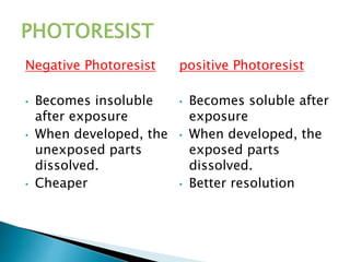
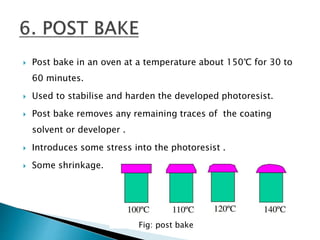
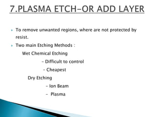
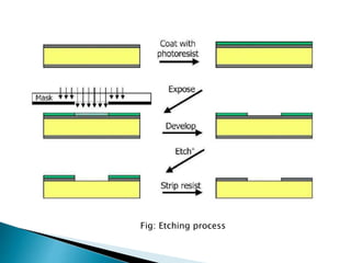
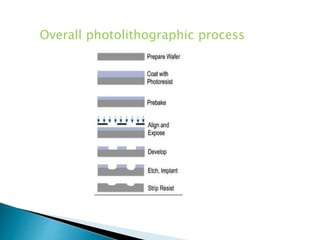
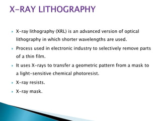
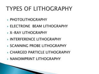
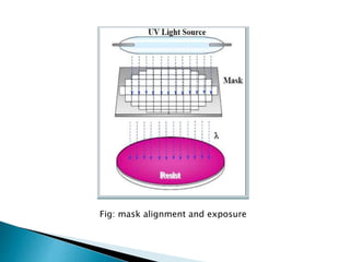
Lithography, originating from the Greek words meaning 'stone' and 'to write', is a technique for transferring geometric shapes onto smooth surfaces, with its modern applications critical in IC manufacturing. It includes various methods such as photolithography, electron beam lithography, and x-ray lithography, each having specific processes and advantages for creating intricate patterns on semiconductor wafers. The process involves several steps including coating with photoresist, exposure, development, and etching, ensuring precise patterning essential for microfabrication.
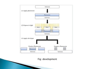
![ The exposed wafer is then put in a developer solution.
The developer solution will remove the exposed or
unexposed regions of photoresist.
Removal of regions depend on the type of photoresist used
[positive or negative resist].](https://image.slidesharecdn.com/lithographytechniquestypes-210224060947/85/Lithography-techniques-types-17-320.jpg)