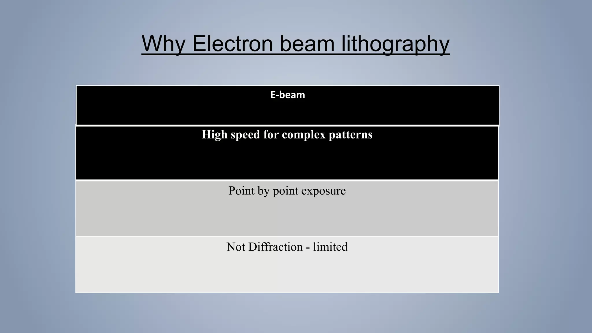
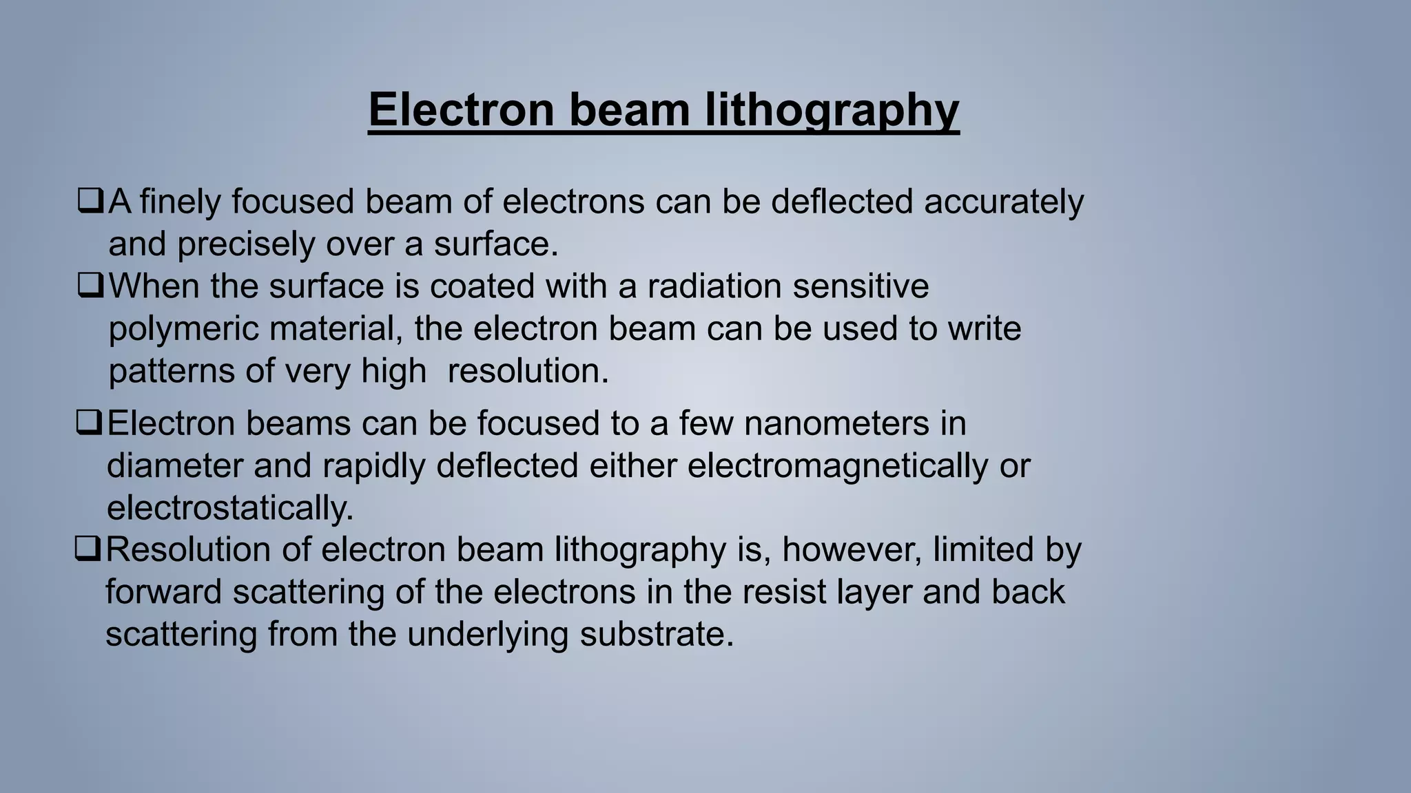
Topic:-
ELECTRON BEAM
LITHOGRAPHY
Prepared by :-
ANJALI VANPARIYA
SAGAR PANELIYA
VISHWA BHAVSAR
Subject:-
Nanostructured Material for Energy Devices
Lithography
 Lithography is also often referred to as photoengraving, and is the process of
transferring a pattern into a reactive polymer film, termed as resist,
Nanostructures Fabricated by Physical Techniques which will subsequently
be used to replicate that pattern into an underlying thin film or substrate.
 Many techniques of lithography have been developed in the last half a century
with various lens systems and exposure radiation sources including photons,
X-rays, electrons, ions and neutral atoms.
Why Electron beam lithography
High speed for complex patterns
Point by point exposure
Not Diffraction - limited
E-beam
Electron beam lithography
A finely focused beam of electrons can be deflected accurately
and precisely over a surface.
When the surface is coated with a radiation sensitive
polymeric material, the electron beam can be used to write
patterns of very high resolution.
Electron beams can be focused to a few nanometers in
diameter and rapidly deflected either electromagnetically or
electrostatically.
Resolution of electron beam lithography is, however, limited by
forward scattering of the electrons in the resist layer and back
scattering from the underlying substrate.
Steps involved in the EBL process
 Exposure of the resist by the forward and backscattered electrons depends on
the beam energy, film thickness and substrate atomic number
When an electron beam enters a polymer film or any solid material, it loses
energy via elastic and inelastic collisions known collectively as electron
scattering.
Elastic collisions result only in a change of direction of the electrons, whereas
inelastic collisions lead to energy loss. These scattering processes lead to a
broadening of the beam
Beam energy increases, the energy loss per unit path length and scattering
cross-sections decreases
 Proper exposure requires that the electron range in the polymer film be
greater than the film thickness in order to ensure exposure of the resist at the
interface.
Electron beam systems can be conveniently considered in two broad
categories:
1. Scanning beam systems have four typical subsystems:
(i) electron source (gun)
(ii) electron column (beam forming system),
(iii) mechanical stage and
(iv) control computer which is used to control the various
machine subsystems and transfer pattern data to the beam
deflection systems.
2. focused electron beams which expose the wafer in serial
fashion, and those projecting an entire pattern simultaneously
onto a wafer.
Electron sources applicable to electron beam lithography are the same as
those used in conventional electron microscopes. These sources can be
divided into 2 groups:
1. Thermionic emission: Thermionic guns rely on the emission of
electrons from a material that is heated above a critical temperature
beyond which electrons are emitted from the surface.
 These sources are prepared from materials such as tungsten,
thoriated
tungsten, or lanthanum hexaboride.
2.Field emission: sources use a highelectric field surrounding a very
sharp point of tungsten.
Advantages:
 The Resolution is not limited by diffraction
 Can write smaller features
 Used to develop specialized device
 No need of physical mask
 Lower deflection densities
 Larger depth of focus due to continuous focussing
Disadvantages:
 Inefficient process for industrial processing
 Long time to pattern entire wafer
 High system cost
 System complexity due to requirement of vacuum
Application
1. Fabrication of masks
2. opto-electronic devices
Electron beam lithography

Electron beam lithography

  • 1.
    Topic:- ELECTRON BEAM LITHOGRAPHY Prepared by:- ANJALI VANPARIYA SAGAR PANELIYA VISHWA BHAVSAR Subject:- Nanostructured Material for Energy Devices
  • 2.
    Lithography  Lithography isalso often referred to as photoengraving, and is the process of transferring a pattern into a reactive polymer film, termed as resist, Nanostructures Fabricated by Physical Techniques which will subsequently be used to replicate that pattern into an underlying thin film or substrate.  Many techniques of lithography have been developed in the last half a century with various lens systems and exposure radiation sources including photons, X-rays, electrons, ions and neutral atoms.
  • 3.
    Why Electron beamlithography High speed for complex patterns Point by point exposure Not Diffraction - limited E-beam
  • 4.
    Electron beam lithography Afinely focused beam of electrons can be deflected accurately and precisely over a surface. When the surface is coated with a radiation sensitive polymeric material, the electron beam can be used to write patterns of very high resolution. Electron beams can be focused to a few nanometers in diameter and rapidly deflected either electromagnetically or electrostatically. Resolution of electron beam lithography is, however, limited by forward scattering of the electrons in the resist layer and back scattering from the underlying substrate.
  • 5.
    Steps involved inthe EBL process
  • 6.
     Exposure ofthe resist by the forward and backscattered electrons depends on the beam energy, film thickness and substrate atomic number When an electron beam enters a polymer film or any solid material, it loses energy via elastic and inelastic collisions known collectively as electron scattering. Elastic collisions result only in a change of direction of the electrons, whereas inelastic collisions lead to energy loss. These scattering processes lead to a broadening of the beam Beam energy increases, the energy loss per unit path length and scattering cross-sections decreases  Proper exposure requires that the electron range in the polymer film be greater than the film thickness in order to ensure exposure of the resist at the interface.
  • 7.
    Electron beam systemscan be conveniently considered in two broad categories: 1. Scanning beam systems have four typical subsystems: (i) electron source (gun) (ii) electron column (beam forming system), (iii) mechanical stage and (iv) control computer which is used to control the various machine subsystems and transfer pattern data to the beam deflection systems. 2. focused electron beams which expose the wafer in serial fashion, and those projecting an entire pattern simultaneously onto a wafer.
  • 8.
    Electron sources applicableto electron beam lithography are the same as those used in conventional electron microscopes. These sources can be divided into 2 groups: 1. Thermionic emission: Thermionic guns rely on the emission of electrons from a material that is heated above a critical temperature beyond which electrons are emitted from the surface.  These sources are prepared from materials such as tungsten, thoriated tungsten, or lanthanum hexaboride. 2.Field emission: sources use a highelectric field surrounding a very sharp point of tungsten.
  • 9.
    Advantages:  The Resolutionis not limited by diffraction  Can write smaller features  Used to develop specialized device  No need of physical mask  Lower deflection densities  Larger depth of focus due to continuous focussing Disadvantages:  Inefficient process for industrial processing  Long time to pattern entire wafer  High system cost  System complexity due to requirement of vacuum
  • 10.
    Application 1. Fabrication ofmasks 2. opto-electronic devices