Downloaded 233 times
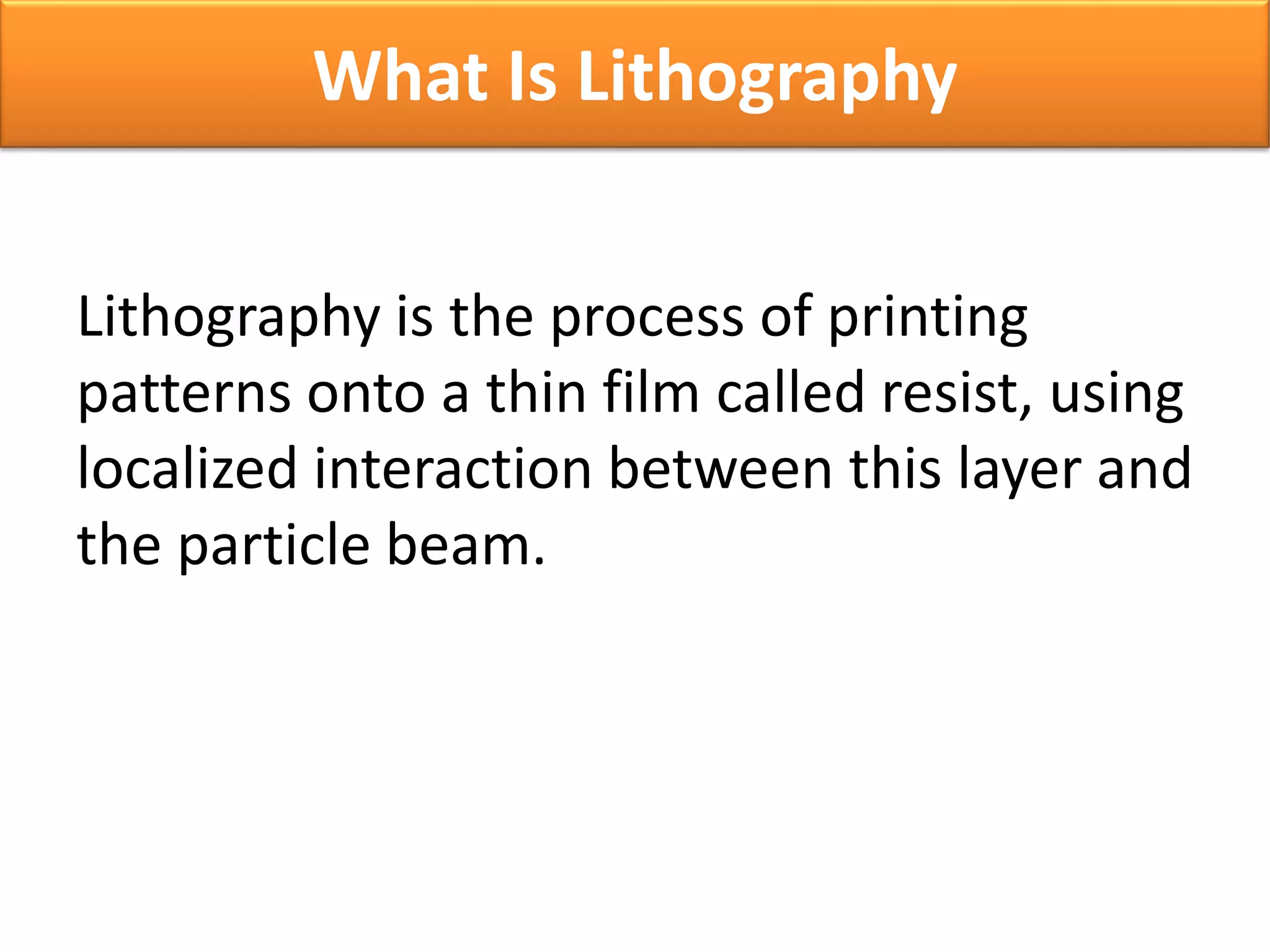
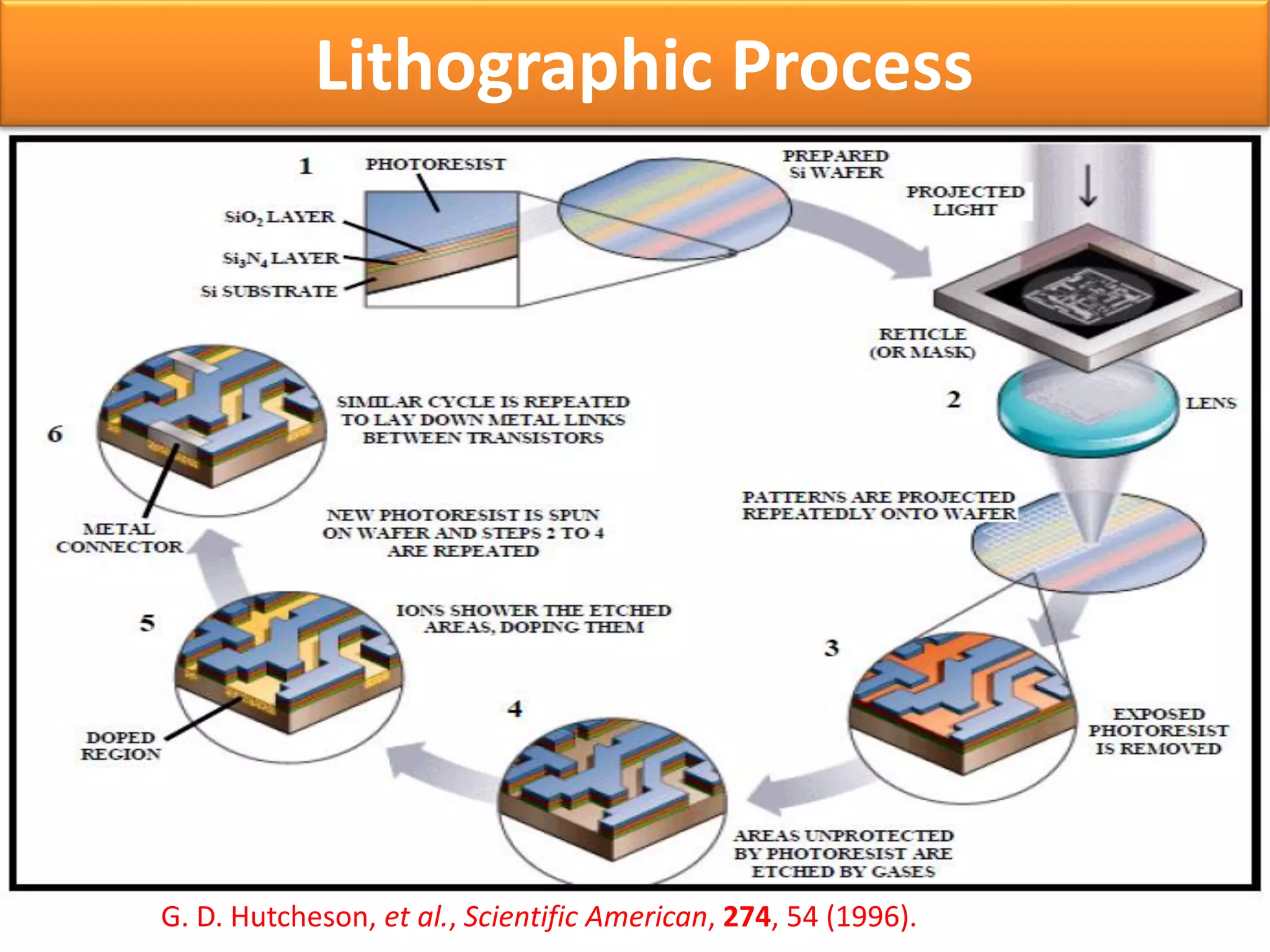
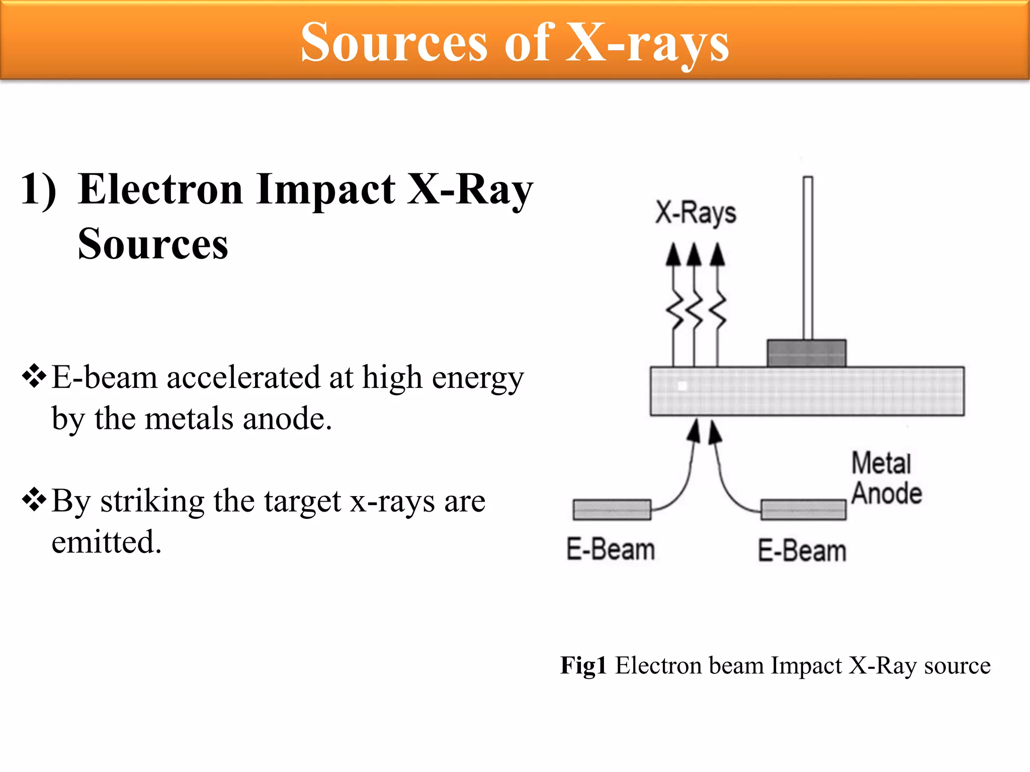
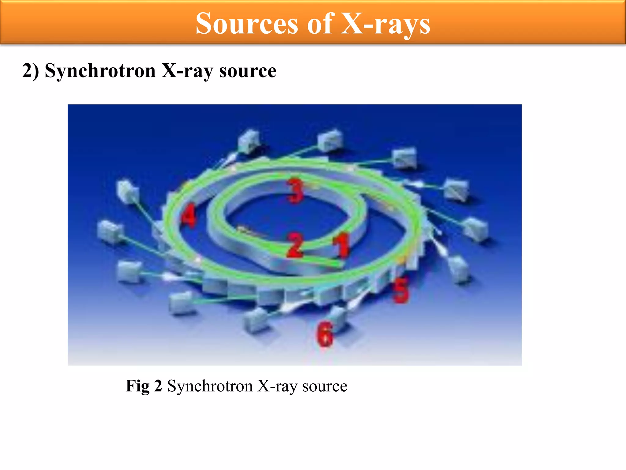
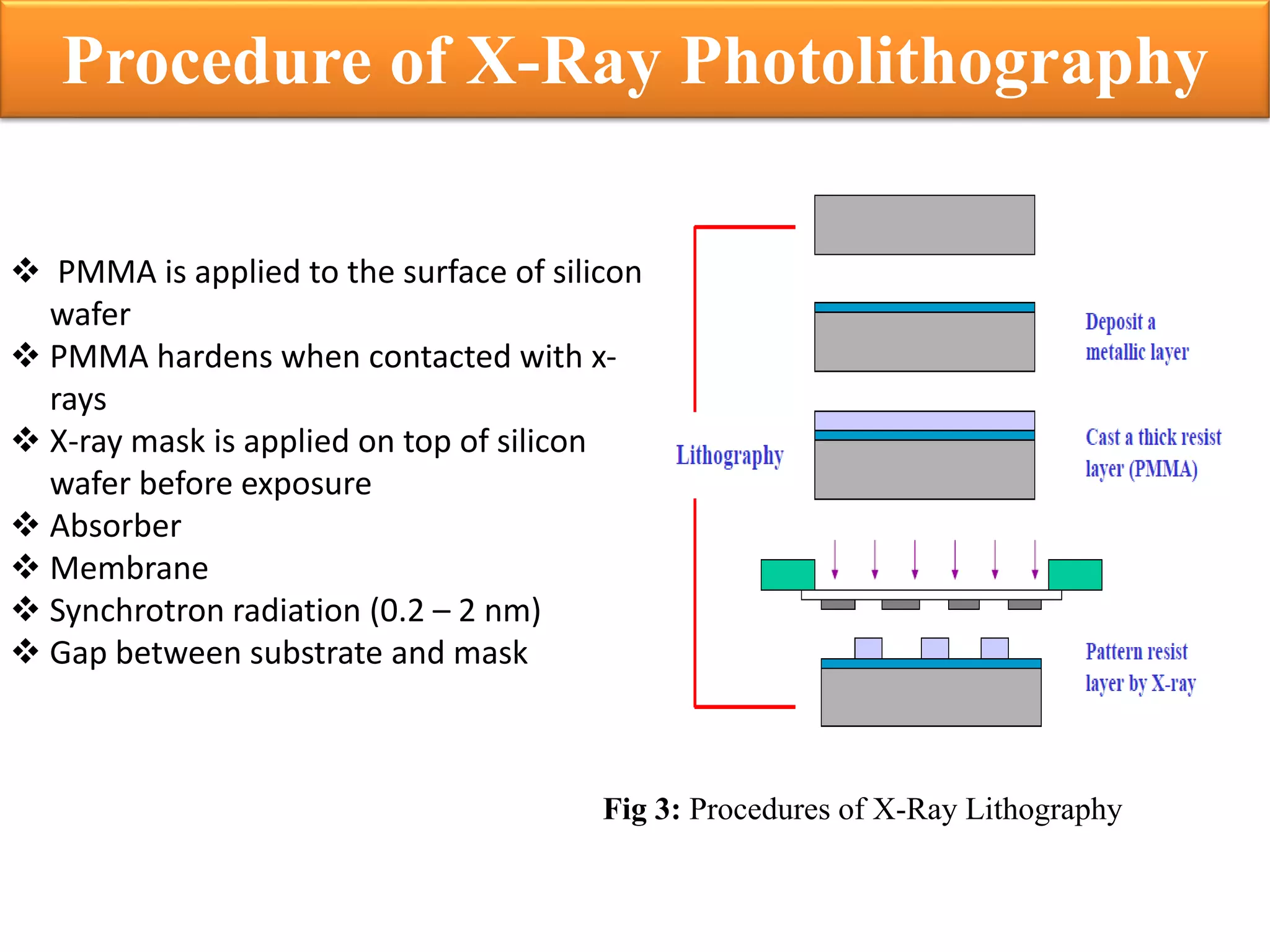
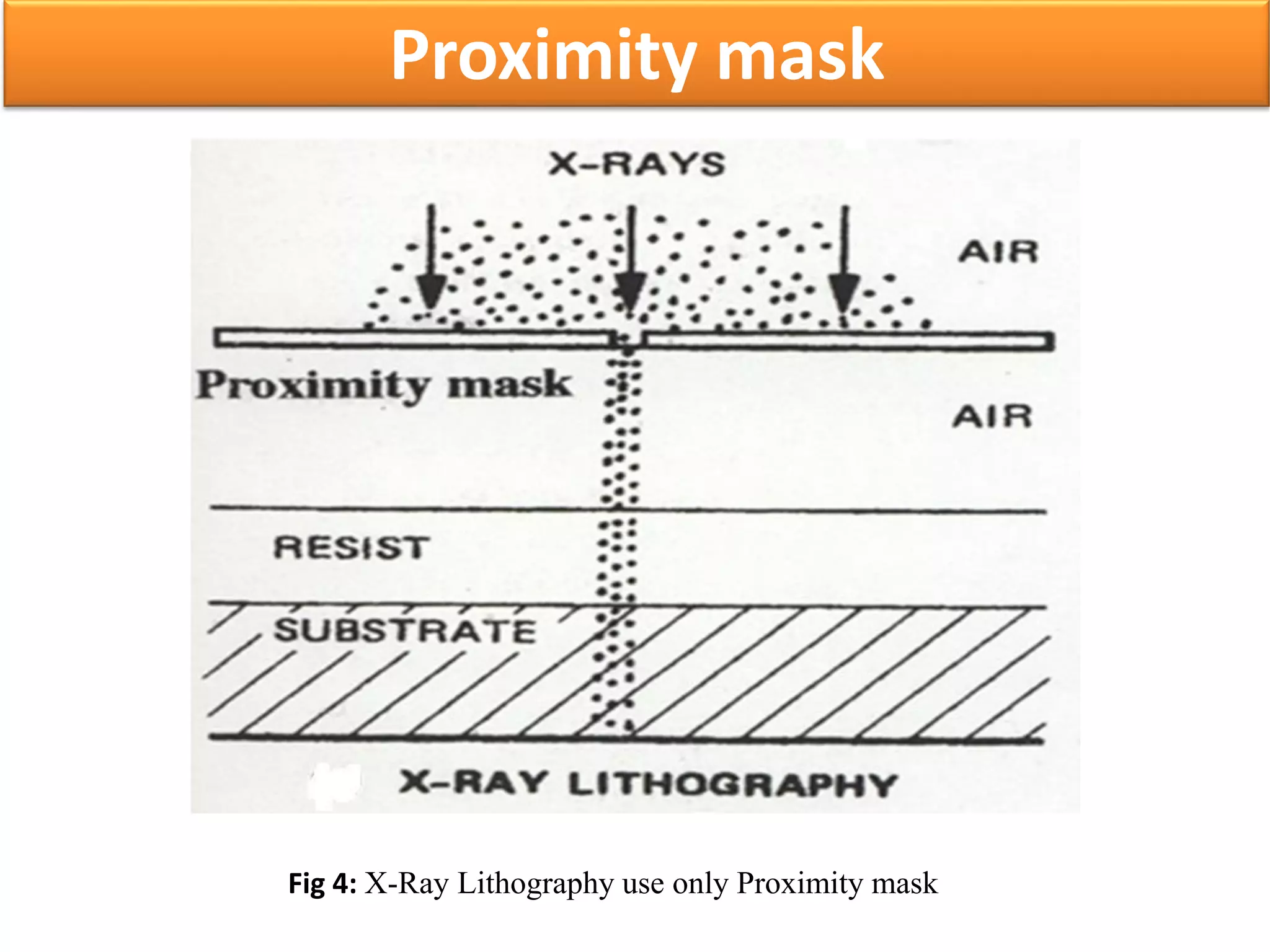
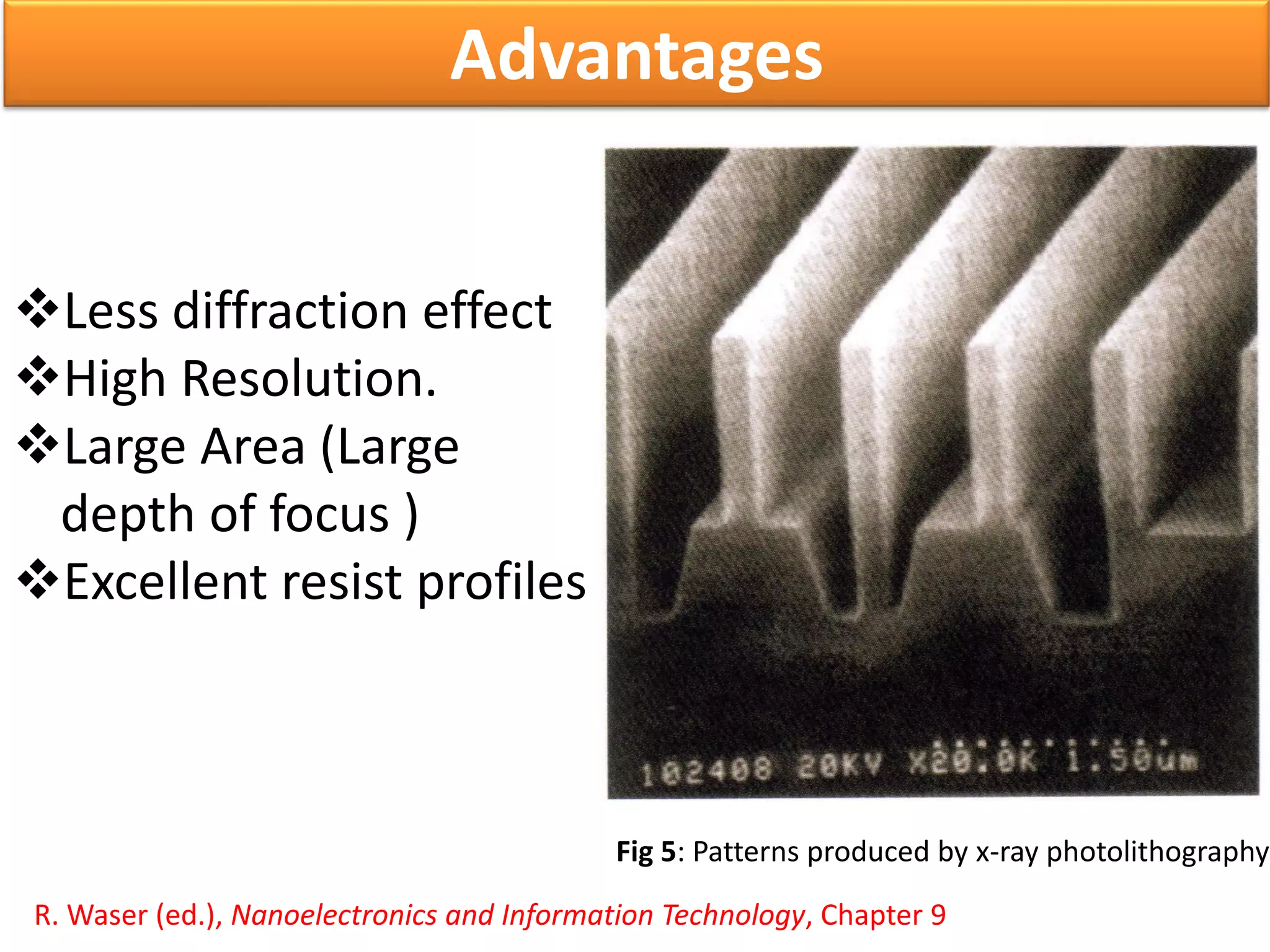
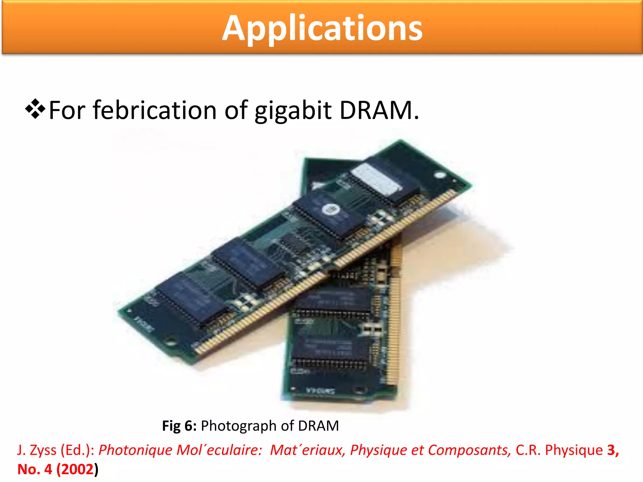
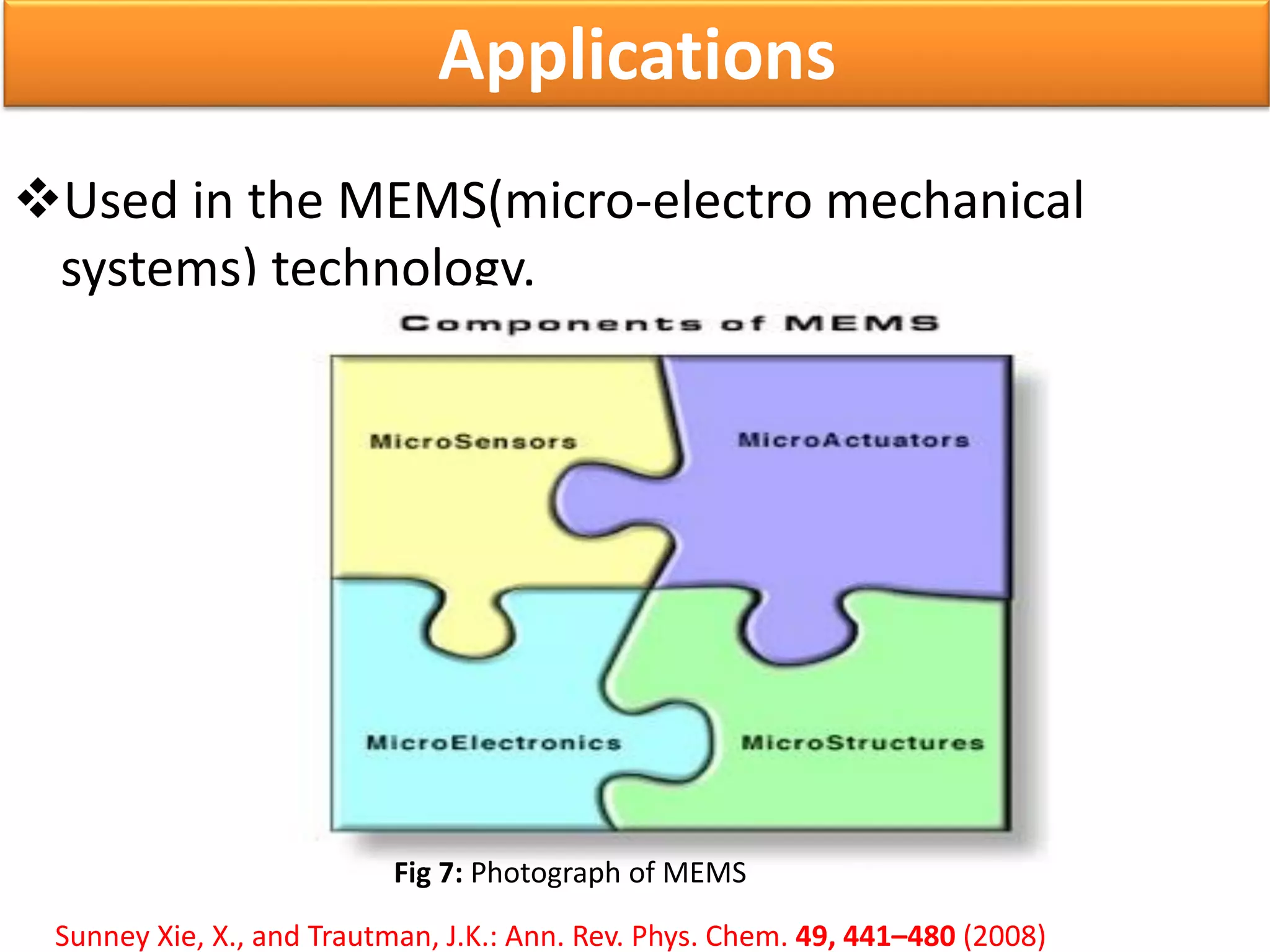


This document discusses x-ray photolithography, which uses x-rays to transfer geometric patterns from a mask to a resist on a substrate. It describes the lithographic process and sources of x-rays, including electron impact and synchrotron sources. The procedure of x-ray photolithography involves applying PMMA resist to a silicon wafer, exposing it to x-rays through an absorber/membrane mask, and developing the pattern. Key advantages are high resolution capability due to less diffraction effects and large depth of focus. Applications include fabrication of gigabit DRAM and MEMS technologies. Limitations include inability to focus x-rays through a lens and high costs of producing masks.