Downloaded 1,257 times

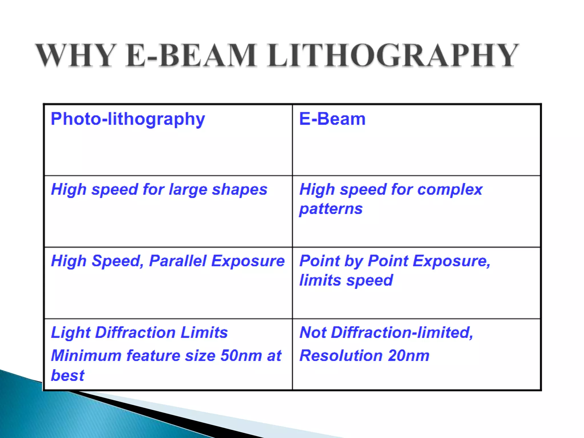


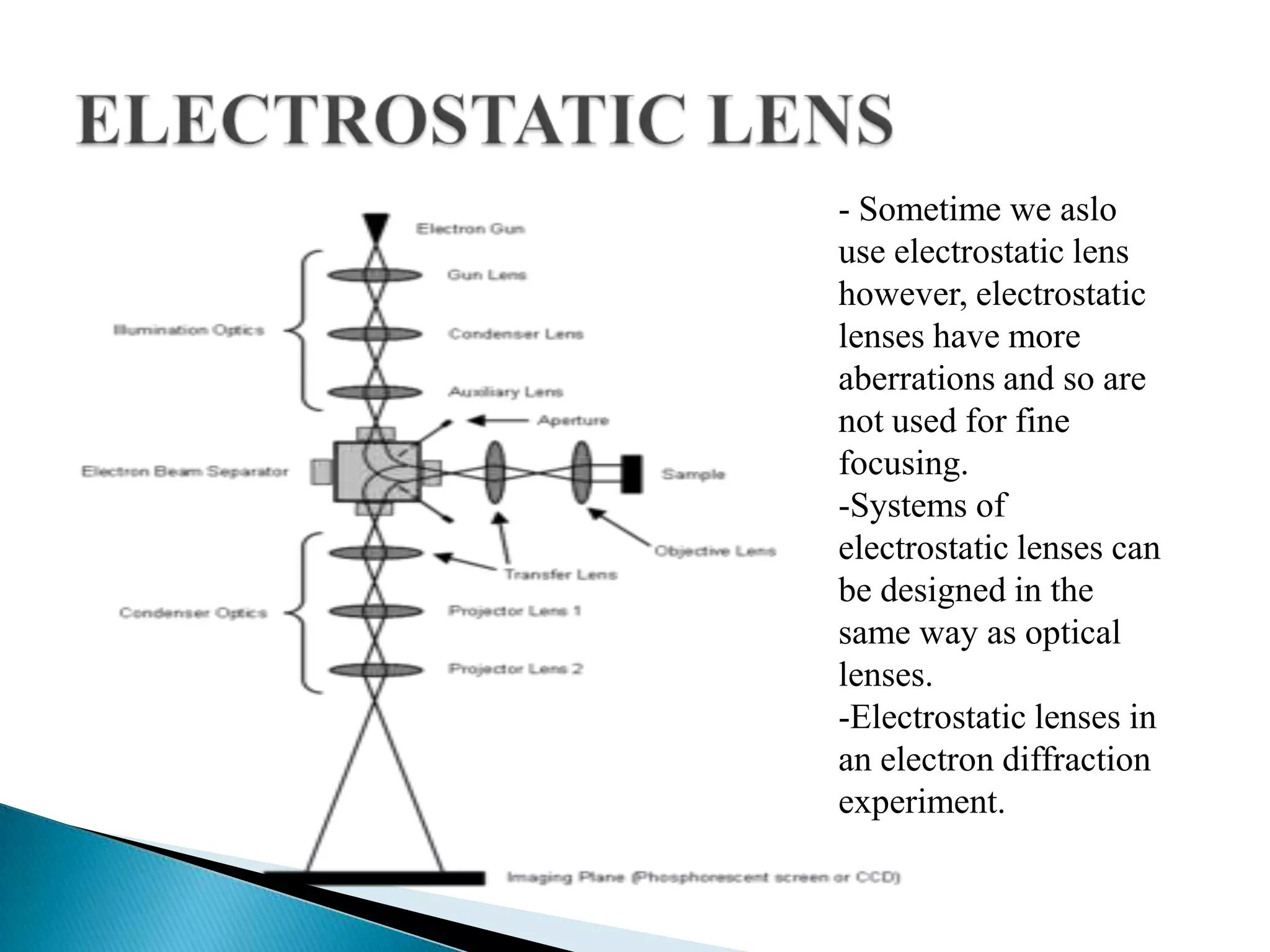


This document discusses electron beam lithography. It begins with an introduction and overview of electron beam lithography, explaining that it uses a beam of electrons to selectively expose and develop a resist film in order to create very small structures. It then provides a schematic of the electron beam lithography process and describes the lithography process steps. The document also covers the advantages of high resolution and no diffraction limit but disadvantages of low throughput and high costs. It includes details on electron beam sources and lenses used.


