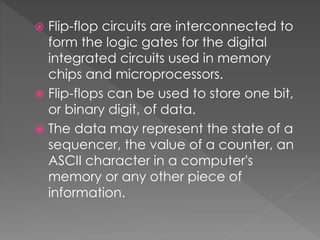
 Flip-flops are digital logic circuits that
can be in one of two states.
 Flip-flops maintain their state indefinitely
until an input pulse called a trigger is
received.
 When a trigger is received, the flip-flop
outputs change state according to
defined rules and remain in those states
until another trigger is received.
 Flip-flop circuits are interconnected to
form the logic gates for the digital
integrated circuits used in memory
chips and microprocessors.
 Flip-flops can be used to store one bit,
or binary digit, of data.
 The data may represent the state of a
sequencer, the value of a counter, an
ASCII character in a computer's
memory or any other piece of
information.
 There are several different kinds of flip-
flop circuits, with designators such as T
(toggle), S-R (set/reset) J-K and D
(delay).
 A flip-flop typically includes zero, one, or
two input signals as well as a clock signal
and an output signal.
 Some flip-flops also include a clear input
signal to reset the current output.
 The SET-RESET flip flop is designed with
the help of two NOR gates and also two
NAND gates.
 The design of such a flip flop includes
two inputs, called the SET [S] and RESET
[R].
 There are also two outputs, Q and Q’.
Logic Diagram Graphic
Symbol
Q S R Q(t+1)
0 0 0 0
0 0 1 0
0 1 0 1
0 1 1 INDETERMINATE
1 0 0 1
1 0 1 0
1 1 0 1
1 1 1 INDETERMINATE
 D flip flop is actually a slight modification
of the above explained clocked SR flip-
flop.
 The D flip-flop tracks the input, making
transitions with match those of the input
D.
 A D flip-flop can be made from
a set/reset flip-flop by tying the set to the
reset through an inverter.
Graphic
Symbol
Logic Diagram
Q D Q(t+1)
0 0 0
0 1 1
1 0 0
1 1 1
 A J-K flip flop can also be defined as a
modification of the S-R flip flop.
 The only difference is that the
intermediate state is more refined and
precise than that of a S-R flip flop.
 The behavior of inputs J and K is same as
the S and R inputs of the S-R flip flop.
 The letter J stands for SET and the letter K
stands for CLEAR.
Logic Diagram Graphic
Symbol
Q J K Q(t+1)
0 0 0 0
0 0 1 0
0 1 0 1
0 1 1 1
1 0 0 1
1 0 1 0
1 1 0 1
1 1 1 0
 This is a much simpler version of the J-K
flip flop. Both the J and K inputs are
connected together and thus are also
called a single input J-K flip flop.
 When clock pulse is given to the flip flop,
the output begins to toggle.
Logic Diagram
Graphic
Symbol
Q T Q(t+1)
0 0 0
0 1 1
1 0 1
1 1 0
 Master-slave flip flop is designed using
two separate flip flops.
 One flip-flop acts as the “Master” circuit,
which triggers on the leading edge of
the clock pulse while the other acts as
the “Slave” circuit, which triggers on the
falling edge of the clock pulse.
Master-Slave flip flop
Q(t) Q(t+1) S R
0 0 0 X
0 1 1 0
1 0 0 1
1 1 X 0
RS Flip Flop
Q(t) Q(t+1) J K
0 0 0 X
0 1 1 X
1 0 X 1
1 1 X 0
J-K Flip Flop
Q(t) Q(t+1) D
0 0 0
0 1 1
1 0 0
1 1 1
D Flip Flop
Q(t) Q(t+1) T
0 0 0
0 1 1
1 0 1
1 1 0
T Flip Flop

What are Flip Flops and Its types.

  • 1.
     Flip-flops aredigital logic circuits that can be in one of two states.  Flip-flops maintain their state indefinitely until an input pulse called a trigger is received.  When a trigger is received, the flip-flop outputs change state according to defined rules and remain in those states until another trigger is received.
  • 2.
     Flip-flop circuitsare interconnected to form the logic gates for the digital integrated circuits used in memory chips and microprocessors.  Flip-flops can be used to store one bit, or binary digit, of data.  The data may represent the state of a sequencer, the value of a counter, an ASCII character in a computer's memory or any other piece of information.
  • 3.
     There areseveral different kinds of flip- flop circuits, with designators such as T (toggle), S-R (set/reset) J-K and D (delay).  A flip-flop typically includes zero, one, or two input signals as well as a clock signal and an output signal.  Some flip-flops also include a clear input signal to reset the current output.
  • 4.
     The SET-RESETflip flop is designed with the help of two NOR gates and also two NAND gates.  The design of such a flip flop includes two inputs, called the SET [S] and RESET [R].  There are also two outputs, Q and Q’.
  • 5.
  • 6.
    Q S RQ(t+1) 0 0 0 0 0 0 1 0 0 1 0 1 0 1 1 INDETERMINATE 1 0 0 1 1 0 1 0 1 1 0 1 1 1 1 INDETERMINATE
  • 7.
     D flipflop is actually a slight modification of the above explained clocked SR flip- flop.  The D flip-flop tracks the input, making transitions with match those of the input D.  A D flip-flop can be made from a set/reset flip-flop by tying the set to the reset through an inverter.
  • 8.
  • 9.
    Q D Q(t+1) 00 0 0 1 1 1 0 0 1 1 1
  • 10.
     A J-Kflip flop can also be defined as a modification of the S-R flip flop.  The only difference is that the intermediate state is more refined and precise than that of a S-R flip flop.  The behavior of inputs J and K is same as the S and R inputs of the S-R flip flop.  The letter J stands for SET and the letter K stands for CLEAR.
  • 11.
  • 12.
    Q J KQ(t+1) 0 0 0 0 0 0 1 0 0 1 0 1 0 1 1 1 1 0 0 1 1 0 1 0 1 1 0 1 1 1 1 0
  • 13.
     This isa much simpler version of the J-K flip flop. Both the J and K inputs are connected together and thus are also called a single input J-K flip flop.  When clock pulse is given to the flip flop, the output begins to toggle.
  • 14.
  • 15.
    Q T Q(t+1) 00 0 0 1 1 1 0 1 1 1 0
  • 16.
     Master-slave flipflop is designed using two separate flip flops.  One flip-flop acts as the “Master” circuit, which triggers on the leading edge of the clock pulse while the other acts as the “Slave” circuit, which triggers on the falling edge of the clock pulse.
  • 17.
  • 18.
    Q(t) Q(t+1) SR 0 0 0 X 0 1 1 0 1 0 0 1 1 1 X 0 RS Flip Flop
  • 19.
    Q(t) Q(t+1) JK 0 0 0 X 0 1 1 X 1 0 X 1 1 1 X 0 J-K Flip Flop
  • 20.
    Q(t) Q(t+1) D 00 0 0 1 1 1 0 0 1 1 1 D Flip Flop
  • 21.
    Q(t) Q(t+1) T 00 0 0 1 1 1 0 1 1 1 0 T Flip Flop