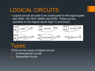
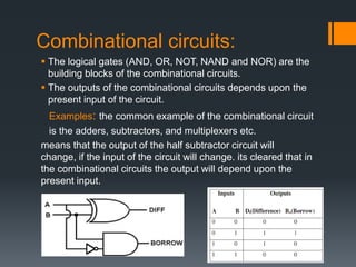
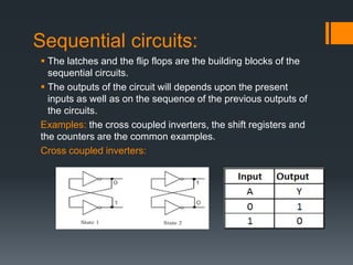
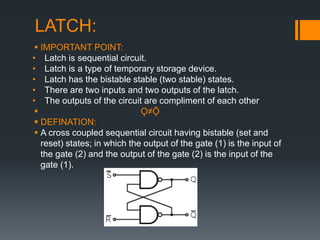
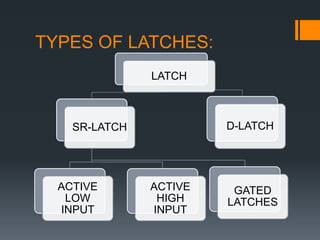
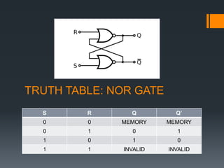
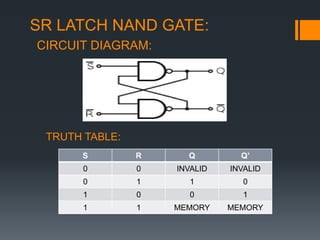
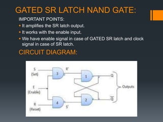
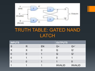
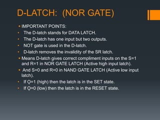
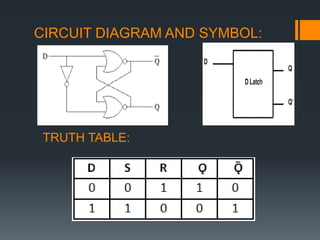
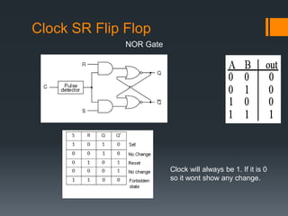
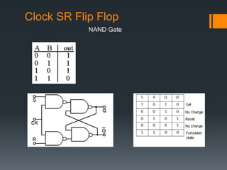
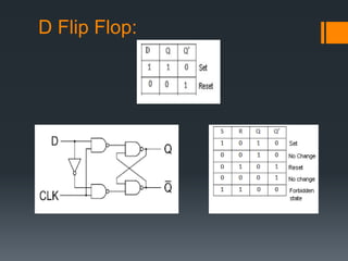
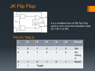
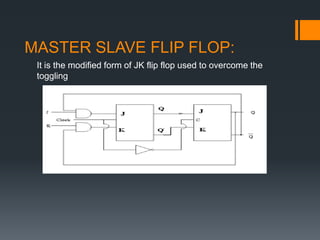
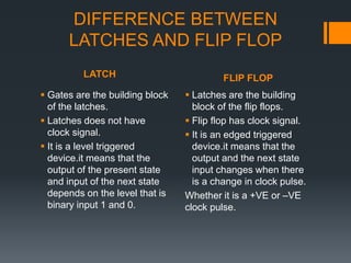
2. LOGICAL CIRCUITS:
Logical circuits are said to be constructed by the logical gates
like (AND, OR ,NOT, NAND and NOR). These circuits
operates on the logical inputs high (1) and low(0).
Types:
There are two types of logical circuits.
1. Combinational circuits.
2. Sequential circuits.
3. Combinational circuits:
The logical gates (AND, OR, NOT, NAND and NOR) are the
building blocks of the combinational circuits.
The outputs of the combinational circuits depends upon the
present input of the circuit.
Examples: the common example of the combinational circuit
is the adders, subtractors, and multiplexers etc.
means that the output of the half subtractor circuit will
change, if the input of the circuit will change. its cleared that in
the combinational circuits the output will depend upon the
present input.
4. Sequential circuits:
The latches and the flip flops are the building blocks of the
sequential circuits.
The outputs of the circuit will depends upon the present
inputs as well as on the sequence of the previous outputs of
the circuits.
Examples: the cross coupled inverters, the shift registers and
the counters are the common examples.
Cross coupled inverters:
5. LATCH:
IMPORTANT POINT:
• Latch is sequential circuit.
• Latch is a type of temporary storage device.
• Latch has the bistable stable (two stable) states.
• There are two inputs and two outputs of the latch.
• The outputs of the circuit are compliment of each other
Ǫ≠Ǭ
DEFINATION:
A cross coupled sequential circuit having bistable (set and
reset) states; in which the output of the gate (1) is the input of
the gate (2) and the output of the gate (2) is the input of the
gate (1).
7. SR LATCHES:
IMPORTANT POINT :
The basic storage element.
There are two inputs R (RESET) and S (SET)
There are Two outputs Q and Q’
Where Q is never equal to Q’ and both are complement of
each other.
The latch of NOR gate is also called the ACTIVE HIGH
INPUT LATCH.
The latch of NAND gate is also called the ACTIVE LOW
INPUT LATCH.
If Q=1 the condition is set
If Q=0 he condition is
reset
8. TRUTH TABLE: NOR GATE
S R Q Q’
0 0 MEMORY MEMORY
0 1 0 1
1 0 1 0
1 1 INVALID INVALID
9. SR LATCH NAND GATE:
CIRCUIT DIAGRAM:
TRUTH TABLE:
S R Q Q’
0 0 INVALID INVALID
0 1 1 0
1 0 0 1
1 1 MEMORY MEMORY
10. GATED SR LATCH NAND GATE:
IMPORTANT POINTS:
It amplifies the SR latch output.
It works with the enable input.
We have enable signal in case of GATED SR latch and clock
signal in case of SR latch.
CIRCUIT DIAGRAM:
11. TRUTH TABLE: GATED NAND
LATCH
INPUTS OUTPUTS
S R EN Q+ Q+’
X X 0 Q Q’
0 0 1 Q Q’
0 1 1 0 1
1 0 1 1 0
1 1 1 INVALID INVALID
12. D-LATCH: (NOR GATE)
IMPORTANT POINTS:
• The D-latch stands for DATA LATCH.
• The D-latch has one input but two outputs.
• NOT gate is used in the D-latch.
• D-latch removes the invalidity of the SR latch.
Means D-latch gives correct compliment inputs on the S=1
and R=1 in NOR GATE LATCH (Active high input latch).
And S=0 and R=0 in NAND GATE LATCH (Active low input
latch).
• If Ǫ=1 (high) then the latch is in the SET state.
• If Ǫ=0 (low) then the latch is in the RESET state.
14. EXPLANATION:
There are two input cases (0 and 1) for the NOT gate as
shown in the TRUTH TABLE of the NOT gate.
Its means that there are two inputs high(0) and low(1) for
D-latch as well.
we need to understand the behavior of the NOR gate.
16. CLOCK PULSE:
a clock signal is a particular type of electrical signal that
oscillates between a high(1) and a low(0) state.
Rise in the signal is high(0) and fall in the signal is the low(1).
The circuit will operates when the CLK signal has high(1)
value. But it depends upon the design of the circuit.
17. The time period is the time from the low signal to the high
signal.
And the frequency of the clock is the inverse of the time
period.
18. FLIP FLOP:
IMPORTANT POINTS:
• The flip flops are sequential circuits.
• Flip flop also stores memory.
• Flip flop also has bistable (two stable) states.
• The outputs are also compliment of each other.
Ǫ≠Ǭ
• Flip flop maintain their states indefinitely until an input pulse
called a (trigger) is received.
DEFINATION:
the flip flop is the bistable multivibrator, having and
regenerative input feedback and used for storing the data in
the form of bits.
25. JK Flip Flop:
It is a modified form of SR Flip Flop
used to over come the forbidden state
(S=1,R=1) of SR.
J K S R Q Q’ Result
1 0 1 0 1 0 Set
0 0 1 0 1 0 No
chang
e
0 1 0 1 0 1 Reset
1 1 Toggle
TRUTH TABLE:
26. MASTER SLAVE FLIP FLOP:
It is the modified form of JK flip flop used to overcome the
toggling
27. Gates are the building block
of the latches.
Latches does not have
clock signal.
It is a level triggered
device.it means that the
output of the present state
and input of the next state
depends on the level that is
binary input 1 and 0.
Latches are the building
block of the flip flops.
Flip flop has clock signal.
It is an edged triggered
device.it means that the
output and the next state
input changes when there
is a change in clock pulse.
Whether it is a +VE or –VE
clock pulse.
DIFFERENCE BETWEEN
LATCHES AND FLIP FLOP
LATCH FLIP FLOP
28. USES OF LATCHES AND FLIP FLOP:
Latches and flip flop are the circuits that store the
information.
Latches and flip flop are the building blocks of the other
complex sequential circuits like shift registers and the
counters etc.
These are used in the computers to store the information like
RAM and Registers.
They can also store one bit, and binary digit of data.