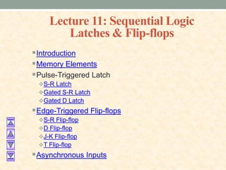
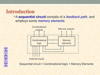
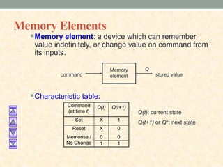
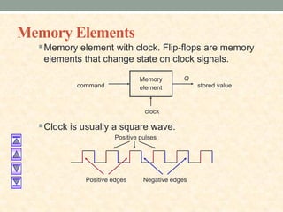
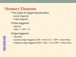
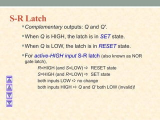
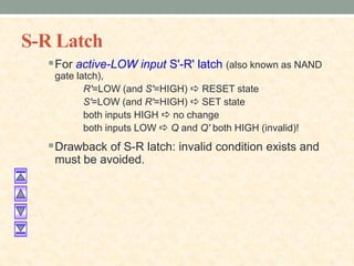
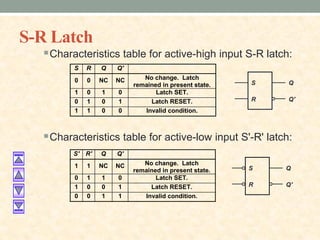
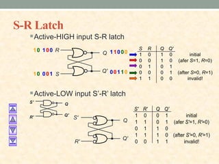
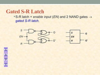
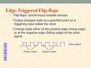
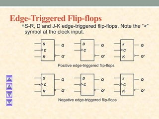
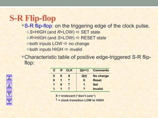
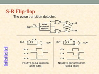
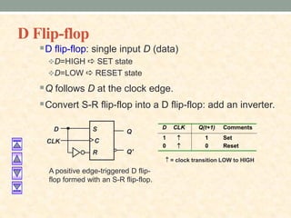
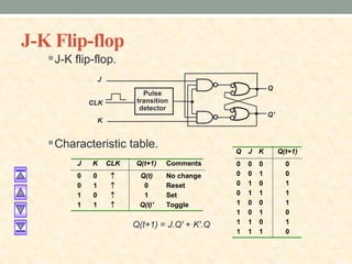
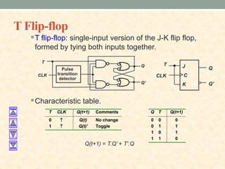
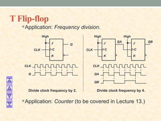
The document discusses sequential logic circuits and memory elements. It describes different types of latches like S-R latch, gated S-R latch and gated D latch. It also explains edge-triggered flip-flops like S-R flip-flop, D flip-flop, J-K flip-flop and T flip-flop. Key differences between latches and flip-flops are that latches change state continuously while flip-flops change state only at the clock edge. Asynchronous inputs like preset and clear are also explained which can directly set or clear the output of a flip-flop.

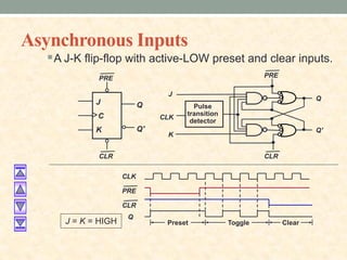
![Asynchronous Inputs
S-R, D and J-K inputs are synchronous inputs, as data
on these inputs are transferred to the flip-flop’s output
only on the triggered edge of the clock pulse.
Asynchronous inputs affect the state of the flip-flop
independent of the clock; example: preset (PRE) and
clear (CLR) [or direct set (SD) and direct reset (RD)]
When PRE=HIGH, Q is immediately set to HIGH.
When CLR=HIGH, Q is immediately cleared to LOW.
Flip-flop in normal operation mode when both PRE
and CLR are LOW.](https://image.slidesharecdn.com/bestslideslatches-221225022726-00c4cf1e/85/best-slides-latches-pdf-28-320.jpg)


![16148_flip-flopaaaaaaaaaaaaaaaaa1[1].ppt](https://cdn.slidesharecdn.com/ss_thumbnails/16148flip-flop11-241007142703-8f186e77-thumbnail.jpg?width=640&height=640&fit=bounds)


![SEQUENTIAL CIRCUITS [FLIP FLOPS AND LATCHES]](https://cdn.slidesharecdn.com/ss_thumbnails/sequentialcircuits-211203044039-thumbnail.jpg?width=640&height=640&fit=bounds)