
Recommended
More Related Content
What's hot
What's hot (20)
Similar to Sequential logic circuit
Similar to Sequential logic circuit (20)
Recently uploaded
Recently uploaded (20)
Sequential logic circuit
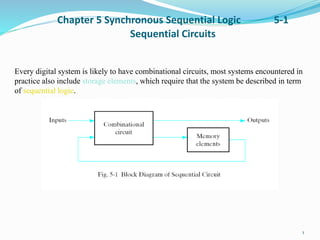
- 1. Chapter 5 Synchronous Sequential Logic 5-1 Sequential Circuits 1 Every digital system is likely to have combinational circuits, most systems encountered in practice also include storage elements, which require that the system be described in term of sequential logic.
- 2. 5-2 Latches SR Latch 2 The SR latch is a circuit with two cross-coupled NOR gates or two cross-coupled NAND gates. It has two inputs labeled S for set and R for reset.
- 3. SR Latch with Control Input 3 The operation of the basic SR latch can be modified by providing an additional control input that determines when the state of the latch can be changed. In Fig. 5-5, it consists of the basic SR latch and two additional NAND gates.
- 4. D Latch 4 One way to eliminate the undesirable condition of the indeterminate state in SR latch is to ensure that inputs S and R are never equal to 1 at the same time in Fig 5-5. This is done in the D latch.
- 5. Graphic Symbols for latches 5 A latch is designated by a rectangular block with inputs on the left and outputs on the right. One output designates the normal output, and the other designates the complement output.
- 6. 5-3 Flip-Flops 6 The state of a latch or flip-flop is switched by a change in the control input. This momentary change is called a trigger and the transition it cause is said to trigger the flip-flop. The D latch with pulses in its control input is essentially a flip-flop that is triggered every time the pulse goes to the logic 1 level. As long as the pulse input remains in the level, any changes in the data input will change the output and the state of the latch.
- 7. Clock Response in Latch 7 InFig (a) a positive level response in the control input allows changes, in the output when the D input changes while the clock pulse stays at logic 1.
- 8. Clock Response in Flip-Flop 8
- 9. Edge-Triggered D Flip-Flop 9 The first latch is called the master and the second the slave. The circuit samples the D input and changes its output Q only at the negative-edge of the controlling clock. CLK D 1 1 0 0 1 1 … Y 1 1 0 0 1 1 … Q ? 1 1 0 0 1 ….
- 10. Graphic Symbol for Edge-Triggered D Flip-Flop 10
- 11. Other Flip-Flops JK Flip-Flop 11 There are three operations that can be performed with a flip-flop: set it to 1, reset it to 0, or complement its output. The JK flip-flop performs all three operations. The circuit diagram of a JK flip-flop constructed with a D flip-flop and gates.
- 12. T Flip-Flop 12 The T flip-flop can be constructed with a D flip-flop and an exclusive-OR gates as shown in Fig. (b). The expression for the D input is D = T Q = TQ` + T`Q
- 13. Characteristic Equations 13 D flip-flop Characteristic Equations Q(t + 1) = D JK flip-flop Characteristic Equations T flip-flop Characteristic Equations Q(t + 1) = JQ` + K`Q Q(t + 1) = T Q = TQ` + T`Q
- 14. Direct Inputs 14 Some flip-flops have asynchronous inputs that are used to force the flip-flop to a particular state independent of the clock. The input that sets the flip-flop to 1 is called present or direct set. The input that clears the flip-flop to 0 is called clear or direct reset. When power is turned on a digital system, the state of the flip-flops is unknown. The direct inputs are useful for bringing all flip-flops in the system to a known starting state prior to the clocked operation.
- 15. D Flip-Flop with Asynchronous Reset 15 A positive-edge-triggered D flip-flop with asynchronous reset is shown in Fig(a).
- 16. D Flip-Flop with Asynchronous Reset 16
- 17. 5-4 Analysis of Clocked Sequential Circuits 17 The analysis of a sequential circuit consists of obtaining a table or a diagram for the time sequence of inputs, outputs, and internal states. It is also possible to write Boolean expressions that describe the behavior of the sequential circuit. These expressions must include the necessary time sequence, either directly or indirectly.
- 18. State Equations 18 The behavior of a clocked sequential circuit can be described algebraically by means of state equations. A state equation specifies the next state as a function of the present state and inputs. Consider the sequential circuit shown in Fig. 5-15. It consists of two D flip-flops A and B, an input x and an output y.
- 19. Fig.5-15 Example of Sequential Circuit 19
- 20. State Equation 20 A(t+1) = A(t) x(t) + B(t) x(t) B(t+1) = A`(t) x(t) A state equation is an algebraic expression that specifies the condition for a flip-flop state transition. The left side of the equation with (t+1) denotes the next state of the flip-flop one clock edge later. The right side of the equation is Boolean expression that specifies the present state and input conditions that make the next state equal to 1. Y(t) = (A(t) + B(t)) x(t)`
- 21. Flip-Flop Input Equations 21 The part of the combinational circuit that generates external outputs is descirbed algebraically by a set of Boolean functions called output equations. The part of the circuit that generates the inputs to flip-flops is described algebraically by a set of Boolean functions called flip-flop input equations. The sequential circuit of Fig. 5-15 consists of two D flip-flops A and B, an input x, and an output y. The logic diagram of the circuit can be expressed algebraically with two flip-flop input equations and an output equation: DA = Ax + Bx DB = A`x y = (A + B)x`
- 22. Analysis with D Flip-Flop 22 The circuit we want to analyze is described by the input equation DA = A x y The DA symbol implies a D flip-flop with output A. The x and y variables are the inputs to the circuit. No output equations are given, so the output is implied to come from the output of the flip-flop.
- 23. Analysis with JK Flip-Flops 23
- 24. Analysis with JK Flip-Flops 24 A(t + 1) = JA` + K`A B(t + 1) = JB` + K`B Substituting the values of JA and KA from the input equations, we obtain the state equation for A: A(t + 1) = BA` + (Bx`)`A = A`B + AB` +Ax The state equation provides the bit values for the column under next state of A in the state table. Similarly, the state equation for flip-flop B can be derived from the characteristic equation by substituting the values of JB and KB: B(t + 1) = x`B` + (A x)`B = B`x` + ABx + A`Bx`
- 25. Analysis With T Flip-Flops 25 Characteristic equation Q(t + 1) = T Q = T`Q + TQ` 00/0 : means state is 00 output is 0
- 26. Mealy and Moore Models (2) 26 Whendealing with the two models, some books and other technical sources refer to a sequential circuit as a finite state machine abbreviated FSM. - The Mealy model of a sequential circuit is referred to as a Mealy FSM or Mealy machine. - The Moore model is refereed to as a Moore FSM or Moore machine.
- 27. 5-5 HDL For Sequential Circuit 27 The Verilog hardware description language (HDL) is introduced in Section 3-9. The description of combinational circuits and an introduction to behavioral modeling is presented in Section 4-11. • In this section, we continue the discussion of the behavioral modeling and present description examples of flip-flops and sequential circuits.
- 28. Behavioral Modeling 28 initial begin clock = 1`b0; repeat (30) #10 clock = ~clock; end initial begin clock = 1`b0; #300 $finish; end always #10 clock = ~clock; There are two kinds of behavioral statements in Verilog HDL: initial and always.
- 29. Behavioral Modeling 29 always @(event control expression) procedural assignment statements. always @(A or B or Reset) always @(posedge clock or negedge reset) The always statement can be controlled by delays that wait for a certain time or by certain conditions to become true or by events to occur.
- 30. 5-6 State Reduction and Assignment 30 • The analysis of sequential circuits starts from a circuit diagram and culminates in a state table or diagram. • The design of a sequential circuit starts from a set of specifications and culminates discusses certain properties of sequential circuits that may be used to reduce the number of gates and flip-flops during the design.
- 31. 5-7 Design Procedure 31 The procedure for designing synchronous sequential circuits can be summarized by a list of recommended steps. 1. From the word description and specifications of the desired operation, derive a state diagram for the circuit. 2. Reduce the number of states if necessary. 3. Assign binary values to the states. 4. Obtain the binary-coded state table. 5. Choose the type of flip-flops to be used. 6. Derive the simplified flip-flop input equations and output equations. 7. Draw the logic diagram.
- 32. Synthesis Using D Flip-Flops 32
- 33. Synthesis Using JK Flip-Flops 33
- 34. Synthesis Using T Flip-Flops 34