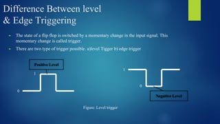
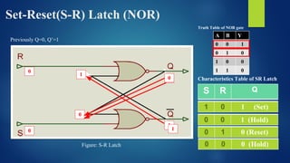
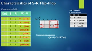
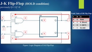
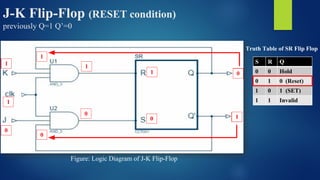
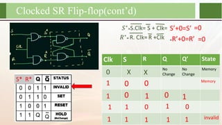
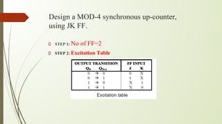
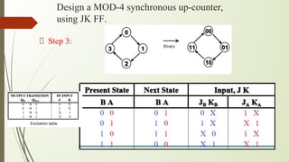
Sequential Circuit
Latches and Flip-Flops
Contents
► Sequential circuit
► Triggering of sequential circuit
► SR latch
► Gated SR latch
► J-K flip-flop
► D flip-flop
► T flip-flop
► Preset Clear JK flip-flop
Sequential Circuit
► Output depends on present input and past history of the system
► Temporary storage device and it has two stable state.
► Two type of sequential circuit :
a) Asynchronous : Output changes any time
b) Synchronous : Output changes with clock
► Level sensitive (Latch)
► Edge triggered (Flip-Flop)
Combinational
Circuit
Memory
Inputs Outputs
clock
Figure: Block diagram of a sequential circuit
Difference Between level
& Edge Triggering
► The state of a flip flop is switched by a momentary change in the input signal. This
momentary change is called trigger.
► There are two type of trigger possible. a)level Tigger b) edge trigger
0
1
0
1
Positive Level
Negative Level
Figure: Level trigger
► Two type of edge trigger.
a) positive edge
b) negative edge
► Positive edge means 0 to 1 transition
► Negative edge means 1 to 0 transition
► Can implement edge trigger by using capacitive coupling (RC circuit is inserted in clock) and
Master Slave flip-flop
Edge Triggering of Flip-Flops
0
1
Positive
Edge
Negative
Edge
0
1
Figure: Edge trigger
Negative
Edge
Positive
Edge
Observation of NOR Gate
A B Y
0 0 1
0 1 0
1 0 0
1 1 0
A
B
Y
Whenever an input is ‘1’ the output Y is ‘0’
Figure: NOR GATE
Truth Table of NOR Gate
Set-Reset(S-R) Latch (NOR)
S R Q
1 0 1(set)
Characteristics Table of SR Latch
Figure: S-R Latch
Let S=1, R=0
1
A B Y
0 0 1
0 1 0
1 0 0
1 1 0
Truth Table of NOR gate
0
0
0
1
1
Set-Reset(S-R) Latch (NOR)
S R Q
1 0 1(set)
Characteristics Table of SR Latch
Figure: S-R Latch
Previously Q=1, Q’=0
0
A B Y
0 0 1
0 1 0
1 0 0
1 1 0
Truth Table of NOR gate
0
0
0
1
1
0 0 1(hold)
0
1
Set-Reset(S-R) Latch (NOR)
S R Q
1 0 1(set)
Characteristics Table of SR Latch
Figure: S-R Latch
Previously Q=1, Q’=0
1
A B Y
0 0 1
0 1 0
1 0 0
1 1 0
Truth Table of NOR gate
0
0
0
1
1
0 0 1(hold)
0
0
0 1 0(reset)
1
Set-Reset(S-R) Latch (NOR)
S R Q
1 0 1 (Set)
Characteristics Table of SR Latch
Figure: S-R Latch
Previously Q=0, Q’=1
0
A B Y
0 0 1
0 1 0
1 0 0
1 1 0
Truth Table of NOR gate
1
1
0
0
0
0 0 1 (Hold)
0 1 0 (Reset)
0 0 0 (Hold)
0
1
Set-Reset(S-R) Latch (NOR)
S R Q
1 0 1 (Set)
Characteristics Table of SR Latch
Figure: S-R Latch
Previously Q=0, Q’=1
1
A B Y
0 0 1
0 1 0
1 0 0
1 1 0
Truth Table of NOR gate
1
1
1
0
0
0 0 1 (Hold)
0 1 0 (Reset)
0 0 0 (Hold)
1 1 Invalid
0
0 0
Set-Reset(S-R) Latch (NOR)
S R Q
1 0 1 (Set)
Characteristics Table of SR Latch
0 0 (Hold)
0 1 0 (Reset)
1 1 Invalid
Block diagram of SR Latch
Q
R
S
time
time
time
Timing diagram of a SR LATCH
Gated Set-Reset(S-R) Latch (NOR)
0
0
0
E S R Q
0 1 0 (Hold)
0 0 0 (Hold)
0 0 1 (Hold)
0 1 1 (Hold)
1
R
S
E S R Q
1 1 0 (SET)
1 0 0 (Hold)
1 0 1 (RESET)
1 1 1 (INVALID)
A B Y
0 0 0
0 1 0
1 0 0
1 1 1
Truth Table of AND gate
Characteristics Table
Gated S-R Latch
Characteristics of S-R Flip-Flop
Q(t) S R Q(t+1)
0 0 0
0 0 1
0 1 0
0 1 1
1 0 0
1 0 1
1 1 0
1 1 1
0 (Hold)
0 (reset)
1 (Set)
(Invalid)
1 (Hold)
0 (reset)
1 (Set)
(Invalid)
x 1
1 x 1
Q(t)
S
R 00 01 11 10
0
1
Characteristics equation:
Q(t+1)=S+ R’Q(t)
Characteristics Table:
S R Q
0 0 Hold
0 1 0 (Reset)
1 0 1 (SET)
1 1 Invalid
S-R Flip-Flop
Characteristics
Characteristics Table
Gated Set-Reset(S-R) Latch (NOR)
E
Gated S-R Latch
R
S
E
Q
time
time
time
time
Timing diagram of a Gated SR LATCH
J-K Flip-Flop
Figure: Logic Diagram of J-K Flip-Flop
• Modified version of S-R
Flip-Flop.
• Enable is replaced with
clock.
• Invalid Condition is
removed
JK Flip Flop
1
0
Q
0
Q
Q
1 0
1
Q
Q
Figure: Logic Diagram of J-K Flip-Flop
J-K Flip-Flop (SET condition)
let Q’=1
S R Q
0 0 Hold
0 1 0 (Reset)
1 0 1 (SET)
1 1 Invalid
1
0 0
1
Q = 1
0
1
1
0
Truth Table of SR Flip Flop
Figure: Logic Diagram of J-K Flip-Flop
J-K Flip-Flop (HOLD condition)
previously Q=1 Q’=0
0 0
1
0
0
1
0
1
0
0
0
S R Q
0 0 Hold
0 1 0 (Reset)
1 0 1 (SET)
1 1 Invalid
1
0
1
0
Truth Table of SR Flip Flop
Figure: Logic Diagram of J-K Flip-Flop
J-K Flip-Flop (RESET condition)
previously Q=1 Q’=0
0
1
1
0
1
0
1
0
0
0
S R Q
0 0 Hold
0 1 0 (Reset)
1 0 1 (SET)
1 1 Invalid
1
0
1
1
0
Truth Table of SR Flip Flop
Figure: Logic Diagram of J-K Flip-Flop
J-K Flip-Flop (Toggle condition)
previously Q=0 Q’=1
0
1
0
1
0
1
0
1
0
1
S R Q
0 0 Hold
0 1 0 (Reset)
1 0 1 (SET)
1 1 Invalid
0
1
1
1
0
Truth Table of SR Flip Flop
Figure: Logic Diagram of J-K Flip-Flop
Characteristics of J-K Flip-Flop
Q(t) J K Q(t+1)
0 0 0
0 0 1
0 1 0
0 1 1
1 0 0
1 0 1
1 1 0
1 1 1
0 (Hold)
0 (reset)
1 (Set)
1 (Toggle)
1 (Hold)
0 (reset)
1 (Set)
0 (Toggle)
1 1
1 1
Q(t)
J
K 00 01 11 10
0
1
Characteristics equation:
Q(t+1)=JK+ K’Q(t)
Characteristics Table:
J K Q
0 0 Hold
0 1 0 (Reset)
1 0 1 (SET)
1 1 Toggle
JK Flip Flop Characteristics
J-K Flip Flop
J K Q
1 0 (Set)
Characteristics table of J-K Flip Flop
0 0 (Hold)
0 1 (Reset)
1 1 Toggle
Block diagram of J-K Flip Flop
K
J
clk
Q
time
time
time
time
Timing diagram of a Gated JK Flip-Flop
D Flip-Flop
J
K
D
Figure: Logic Diagram of D Flip-Flop
D Flip-Flop
D
K
J
Q
Q
Block diagram of D Flip Flop
J K Q
1 0 (Set)
Characteristics table
of J-K Flip-Flop
0 0 (Hold)
0 1 (Reset)
1 1 Toggle
D Q
0 0
1 1
0
1
0
1 0
1
1
1
0
0 1
0
Characteristics table of D
Flip-Flop
J-K
Flip Flop
clk
N.B. INPUT AND OUTPUT SAME SO ACTS AS A BUFFER
CIRCUIT
Characteristics of D Flip Flop
Q(t) D Q(t+1)
0 0
0 1
1 0
1 1
0
1
0
1
1
1
Q(t)
D
0 1
0
1
Characteristics equation:
Q(t+1)=D
Characteristics Table: D Q
0 0
1 1
D Flip Flop Characteristics
D Flip-Flop
D Q
0 0
1 1
Characteristics table of D Flip-Flop
D
Q
Q
Block diagram of D Flip Flop
D
Flip Flop
clk
D
clk
Q
time
time
time
Timing diagram of a Gated D Flip-Flop
T Flip-Flop
T
Figure: Logic Diagram of T Flip-Flop
T Flip-Flop
T
K
J
Q
Q
Block diagram of T Flip Flop
J K Q
1 0 (Set)
Characteristics table
of J-K Flip-Flop
0 0 (Hold)
0 1 (Reset)
1 1 Toggle
T Q
0 HOLD
1 Toggle
1
1
Toggle
Characteristics table of T
Flip-Flop
J-K
Flip Flop
clk
1
0
0
0
Hold
Characteristics of T Flip Flop
Q(t) T Q(t+1)
0 0
0 1
1 0
1 1
0 (HOLD)
1
(TOGGLE)
1 (HOLD)
0
(TOGGLE)
1
1
Q(t)
T
0 1
0
1
Characteristics equation:
Q(t+1) = T Q(t)’ + T’ Q(t)
Characteristics Table: T Q
0 HOLD
1 TOGGLE
D Flip Flop Characteristics
T Flip-Flop
T
Q
Q
Block diagram of T Flip Flop
T
Flip Flop
clk
time
time
T Q
0 HOLD
1 Toggle
Characteristics table of T
Flip-Flop
The
End
Green University of Bangladesh
Department of Electrical & Electronic Engineering
Sequential Circuit
Triggering of Flip-flop
Combinational
Circuit
Memory
Clock Pulse
Input Output
State
Latch/Flipflop
Control Input
Triggering of Flip-flop
❑ Edge Trigger
❑ Level Trigger
Triggering of Flip-flop
❑ Level Trigger ❑ Edge Trigger
The flip flop is triggered only during the
high-level or the low level of the clock pulse.
Positive level triggering
Negative level triggering
In edge triggering, the flip flop changes its state during
the positive edge or negative edge of the clock pulse.
Positive edge triggering
Negative edge triggering
Triggering of Flip-flop
Clocked SR Flip-flop
SR Flip flop with Clock Nand Latch
Clocked SR Flip-flop(cont’d)
This whole Circuit is SR Flip-Flop
Clocked SR Flip-flop(cont’d)
Clk S R Q Q’ State
No
Change
No
Change
Memory
0 X X
S’+ 1= 1
=R’+ 1=1
S* R*
Clocked SR Flip-flop(cont’d)
Clk S R Q Q’ State
No
Change
No
Change
Memory
0 X X
S’+0=S’
=R’+0=R’
S* R*
1 0 0
=1
=1
Memory
Clocked SR Flip-flop(cont’d)
Clk S R Q Q’ State
No
Change
No
Change
Memory
0 X X
S’+0=S’
=R’+0=R’
S* R*
1 0 0
=1
=0
Memory
1 0 1 0 1
Clocked SR Flip-flop(cont’d)
Clk S R Q Q’ State
No
Change
No
Change
Memory
0 X X
S’+0=S’
=R’+0=R’
S* R*
1 0 0
=0
=1
Memory
1 0 1 0 1
1 1 0 1 0
Clocked SR Flip-flop(cont’d)
Clk S R Q Q’ State
No
Change
No
Change
Memory
0 X X
S’+0=S’
=R’+0=R’
S* R*
1 0 0
=0
=0
Memory
1 0 1 0 1
1 1 0 1 0
1 1 1 1 1 invalid
Truth Table for Clocked SR Flipflop(cont’d)
Clk S R Q Q’ State
No
Change
No
Change
Memory
0 X X
1 0 0 Memory
1 0 1 0 1
1 1 0 1 0
1 1 1 1 1 invalid
❑ Circuit ❑ Truth Table
Truth Table for Clocked SR Flipflop(cont’d)
Clk S R Qn+1
Qn
Qn
0 X X
1 0 0
1 0 1 0
1 1 0 1
1 1 1 X
❑ Characteristic Table ❑ Truth Table
Qn S R Qn+1
0 0 0 0
0 0 1 0
0 1 0 1
0 1 1 X
1 0 0 1
1 0 1 0
1 1 0 1
1 1 1 X
Truth Table for Clocked SR Flipflop(cont’d)
❑ Characteristic Table ❑ Excitation Table
❑ Truth Table for SR flipflop
D flip-flop
❑ Truth Table for SR flipflop
D flip-flop
❑ Truth Table for D flip-flop
D flip-flop
D flip-flop
Synchronous Counter
Definition
A synchronous counter , in contrast to an
asynchronous counter , is one whose output bits
change state simultaneously, with no ripple.
The only way we can build such a counter circuit from J-K flip-flops
is to connect all the clock inputs together, so that each and every
flip-flop receives the exact same clock pulse at the exact same time
Now, the question is, what do we do with the J and K inputs? We know that we still have to
maintain the same divide-by-two frequency pattern in order to count in a binary sequence, and
that this pattern is best achieved utilizing the "toggle" mode of the flip-flop, so the fact that the
J and K inputs must both be (at times) "high" is clear. However, if we simply connect all the J
and K inputs to the positive rail of the power supply as we did in the asynchronous circuit, this
would clearly not work because all the flip-flops would toggle at the same time: with each and
every clock pulse!
How To Design Synchronous Counter
Design a MOD-4 synchronous up-counter,
using JK FF.
STEP 1: No of FF=2
STEP 2: Excitation Table
Design a MOD-4 synchronous up-counter,
using JK FF.
Step 3:
Step 4: Obtain the simplified function using K-Map
B
A
B
B
B
A
A
A
Step 5: Draw the circuit diagram.
Design a MOD-8 synchronous up-counter,
using JK FF.
Step2: State transition diagram & State
Table
Step 3: Expand the present state-next state table to form the transition
table.
Excitation Table
Step 4: Use Karnaugh maps to identify the present state
logic functions for each of the inputs.
QB QA
QC
QB QA
QC
QC
QB QA
Circuit Implementation
How To Design Synchronous Counter
that count Random number
Design a Synchronous Counter to Count 4,7,3,0 and 2 respectively using
JKFlip Flop negative trigered by showing:
i. Flip Flop Used
ii. State Transition Diagram
iii. Exitation Table / Present state, next State
iv. Karnough Map & perform Simplified Function
v. The Synchronous Counter
n = 3 bit = 3 Flip Flop
Synchronous Counter to Count 4,7,3,0 and 2 respectively
Step 4: Karnough Map and
Simplified Function
K Map for JA
0 0 1X 3 X 2 0
4 1 5X 7 X 6 X
BA
C
4=100
5=101
7=111
6=110
C B A
JA= C=QC
Step 4: Karnough Map and
Simplified Function
K Map for KA
0 X 1X 3 1 2 X
4 X 5X 7 0 6 X
BA
C
0=000
1=001
3=011
2=010
C B A
KA= C=QC
Step 4: Karnough Map and
Simplified Function
K Map for JB
0 1 1X 3 X 2 X
4 1 5X 7 X 6 X
BA
C
JB=1
Step 4: Karnough Map and
Simplified Function
K Map for KB
0 X 1X 3 1 2 1
4 X 5X 7 0 6 X
BA
C
0=000
1=001
3=011
2=010
C B A
KB= C=QC
Step 4: Karnough Map and
Simplified Function
K Map for Jc
0 0 1X 3 0 2 1
4 X 5X 7 X 6 X
BA
C
2=010
6=110
C B A
Jc= BA=QBQA
Step 4: Karnough Map and
Simplified Function
K Map for Kc
0 X 1X 3 X 2 X
4 0 5X 7 1 6 X
BA
C
2=010
3=011
7=111
6=110
C B A
Kc= B=QB
Circuit Implementation
C
B
A
Sequential circuit latchs and Flip-Flops.

Sequential circuit latchs and Flip-Flops.

  • 1.
  • 2.
    Contents ► Sequential circuit ►Triggering of sequential circuit ► SR latch ► Gated SR latch ► J-K flip-flop ► D flip-flop ► T flip-flop ► Preset Clear JK flip-flop
  • 3.
    Sequential Circuit ► Outputdepends on present input and past history of the system ► Temporary storage device and it has two stable state. ► Two type of sequential circuit : a) Asynchronous : Output changes any time b) Synchronous : Output changes with clock ► Level sensitive (Latch) ► Edge triggered (Flip-Flop) Combinational Circuit Memory Inputs Outputs clock Figure: Block diagram of a sequential circuit
  • 4.
    Difference Between level &Edge Triggering ► The state of a flip flop is switched by a momentary change in the input signal. This momentary change is called trigger. ► There are two type of trigger possible. a)level Tigger b) edge trigger 0 1 0 1 Positive Level Negative Level Figure: Level trigger
  • 5.
    ► Two typeof edge trigger. a) positive edge b) negative edge ► Positive edge means 0 to 1 transition ► Negative edge means 1 to 0 transition ► Can implement edge trigger by using capacitive coupling (RC circuit is inserted in clock) and Master Slave flip-flop Edge Triggering of Flip-Flops 0 1 Positive Edge Negative Edge 0 1 Figure: Edge trigger Negative Edge Positive Edge
  • 6.
    Observation of NORGate A B Y 0 0 1 0 1 0 1 0 0 1 1 0 A B Y Whenever an input is ‘1’ the output Y is ‘0’ Figure: NOR GATE Truth Table of NOR Gate
  • 7.
    Set-Reset(S-R) Latch (NOR) SR Q 1 0 1(set) Characteristics Table of SR Latch Figure: S-R Latch Let S=1, R=0 1 A B Y 0 0 1 0 1 0 1 0 0 1 1 0 Truth Table of NOR gate 0 0 0 1 1
  • 8.
    Set-Reset(S-R) Latch (NOR) SR Q 1 0 1(set) Characteristics Table of SR Latch Figure: S-R Latch Previously Q=1, Q’=0 0 A B Y 0 0 1 0 1 0 1 0 0 1 1 0 Truth Table of NOR gate 0 0 0 1 1 0 0 1(hold) 0 1
  • 9.
    Set-Reset(S-R) Latch (NOR) SR Q 1 0 1(set) Characteristics Table of SR Latch Figure: S-R Latch Previously Q=1, Q’=0 1 A B Y 0 0 1 0 1 0 1 0 0 1 1 0 Truth Table of NOR gate 0 0 0 1 1 0 0 1(hold) 0 0 0 1 0(reset) 1
  • 10.
    Set-Reset(S-R) Latch (NOR) SR Q 1 0 1 (Set) Characteristics Table of SR Latch Figure: S-R Latch Previously Q=0, Q’=1 0 A B Y 0 0 1 0 1 0 1 0 0 1 1 0 Truth Table of NOR gate 1 1 0 0 0 0 0 1 (Hold) 0 1 0 (Reset) 0 0 0 (Hold) 0 1
  • 11.
    Set-Reset(S-R) Latch (NOR) SR Q 1 0 1 (Set) Characteristics Table of SR Latch Figure: S-R Latch Previously Q=0, Q’=1 1 A B Y 0 0 1 0 1 0 1 0 0 1 1 0 Truth Table of NOR gate 1 1 1 0 0 0 0 1 (Hold) 0 1 0 (Reset) 0 0 0 (Hold) 1 1 Invalid 0 0 0
  • 12.
    Set-Reset(S-R) Latch (NOR) SR Q 1 0 1 (Set) Characteristics Table of SR Latch 0 0 (Hold) 0 1 0 (Reset) 1 1 Invalid Block diagram of SR Latch Q R S time time time Timing diagram of a SR LATCH
  • 13.
    Gated Set-Reset(S-R) Latch(NOR) 0 0 0 E S R Q 0 1 0 (Hold) 0 0 0 (Hold) 0 0 1 (Hold) 0 1 1 (Hold) 1 R S E S R Q 1 1 0 (SET) 1 0 0 (Hold) 1 0 1 (RESET) 1 1 1 (INVALID) A B Y 0 0 0 0 1 0 1 0 0 1 1 1 Truth Table of AND gate Characteristics Table Gated S-R Latch
  • 14.
    Characteristics of S-RFlip-Flop Q(t) S R Q(t+1) 0 0 0 0 0 1 0 1 0 0 1 1 1 0 0 1 0 1 1 1 0 1 1 1 0 (Hold) 0 (reset) 1 (Set) (Invalid) 1 (Hold) 0 (reset) 1 (Set) (Invalid) x 1 1 x 1 Q(t) S R 00 01 11 10 0 1 Characteristics equation: Q(t+1)=S+ R’Q(t) Characteristics Table: S R Q 0 0 Hold 0 1 0 (Reset) 1 0 1 (SET) 1 1 Invalid S-R Flip-Flop Characteristics
  • 15.
    Characteristics Table Gated Set-Reset(S-R)Latch (NOR) E Gated S-R Latch R S E Q time time time time Timing diagram of a Gated SR LATCH
  • 16.
    J-K Flip-Flop Figure: LogicDiagram of J-K Flip-Flop • Modified version of S-R Flip-Flop. • Enable is replaced with clock. • Invalid Condition is removed
  • 17.
    JK Flip Flop 1 0 Q 0 Q Q 10 1 Q Q Figure: Logic Diagram of J-K Flip-Flop
  • 18.
    J-K Flip-Flop (SETcondition) let Q’=1 S R Q 0 0 Hold 0 1 0 (Reset) 1 0 1 (SET) 1 1 Invalid 1 0 0 1 Q = 1 0 1 1 0 Truth Table of SR Flip Flop Figure: Logic Diagram of J-K Flip-Flop
  • 19.
    J-K Flip-Flop (HOLDcondition) previously Q=1 Q’=0 0 0 1 0 0 1 0 1 0 0 0 S R Q 0 0 Hold 0 1 0 (Reset) 1 0 1 (SET) 1 1 Invalid 1 0 1 0 Truth Table of SR Flip Flop Figure: Logic Diagram of J-K Flip-Flop
  • 20.
    J-K Flip-Flop (RESETcondition) previously Q=1 Q’=0 0 1 1 0 1 0 1 0 0 0 S R Q 0 0 Hold 0 1 0 (Reset) 1 0 1 (SET) 1 1 Invalid 1 0 1 1 0 Truth Table of SR Flip Flop Figure: Logic Diagram of J-K Flip-Flop
  • 21.
    J-K Flip-Flop (Togglecondition) previously Q=0 Q’=1 0 1 0 1 0 1 0 1 0 1 S R Q 0 0 Hold 0 1 0 (Reset) 1 0 1 (SET) 1 1 Invalid 0 1 1 1 0 Truth Table of SR Flip Flop Figure: Logic Diagram of J-K Flip-Flop
  • 22.
    Characteristics of J-KFlip-Flop Q(t) J K Q(t+1) 0 0 0 0 0 1 0 1 0 0 1 1 1 0 0 1 0 1 1 1 0 1 1 1 0 (Hold) 0 (reset) 1 (Set) 1 (Toggle) 1 (Hold) 0 (reset) 1 (Set) 0 (Toggle) 1 1 1 1 Q(t) J K 00 01 11 10 0 1 Characteristics equation: Q(t+1)=JK+ K’Q(t) Characteristics Table: J K Q 0 0 Hold 0 1 0 (Reset) 1 0 1 (SET) 1 1 Toggle JK Flip Flop Characteristics
  • 23.
    J-K Flip Flop JK Q 1 0 (Set) Characteristics table of J-K Flip Flop 0 0 (Hold) 0 1 (Reset) 1 1 Toggle Block diagram of J-K Flip Flop K J clk Q time time time time Timing diagram of a Gated JK Flip-Flop
  • 24.
    D Flip-Flop J K D Figure: LogicDiagram of D Flip-Flop
  • 25.
    D Flip-Flop D K J Q Q Block diagramof D Flip Flop J K Q 1 0 (Set) Characteristics table of J-K Flip-Flop 0 0 (Hold) 0 1 (Reset) 1 1 Toggle D Q 0 0 1 1 0 1 0 1 0 1 1 1 0 0 1 0 Characteristics table of D Flip-Flop J-K Flip Flop clk N.B. INPUT AND OUTPUT SAME SO ACTS AS A BUFFER CIRCUIT
  • 26.
    Characteristics of DFlip Flop Q(t) D Q(t+1) 0 0 0 1 1 0 1 1 0 1 0 1 1 1 Q(t) D 0 1 0 1 Characteristics equation: Q(t+1)=D Characteristics Table: D Q 0 0 1 1 D Flip Flop Characteristics
  • 27.
    D Flip-Flop D Q 00 1 1 Characteristics table of D Flip-Flop D Q Q Block diagram of D Flip Flop D Flip Flop clk D clk Q time time time Timing diagram of a Gated D Flip-Flop
  • 28.
    T Flip-Flop T Figure: LogicDiagram of T Flip-Flop
  • 29.
    T Flip-Flop T K J Q Q Block diagramof T Flip Flop J K Q 1 0 (Set) Characteristics table of J-K Flip-Flop 0 0 (Hold) 0 1 (Reset) 1 1 Toggle T Q 0 HOLD 1 Toggle 1 1 Toggle Characteristics table of T Flip-Flop J-K Flip Flop clk 1 0 0 0 Hold
  • 30.
    Characteristics of TFlip Flop Q(t) T Q(t+1) 0 0 0 1 1 0 1 1 0 (HOLD) 1 (TOGGLE) 1 (HOLD) 0 (TOGGLE) 1 1 Q(t) T 0 1 0 1 Characteristics equation: Q(t+1) = T Q(t)’ + T’ Q(t) Characteristics Table: T Q 0 HOLD 1 TOGGLE D Flip Flop Characteristics
  • 31.
    T Flip-Flop T Q Q Block diagramof T Flip Flop T Flip Flop clk time time T Q 0 HOLD 1 Toggle Characteristics table of T Flip-Flop
  • 32.
  • 33.
    Green University ofBangladesh Department of Electrical & Electronic Engineering Sequential Circuit
  • 34.
    Triggering of Flip-flop Combinational Circuit Memory ClockPulse Input Output State Latch/Flipflop Control Input
  • 35.
    Triggering of Flip-flop ❑Edge Trigger ❑ Level Trigger
  • 36.
    Triggering of Flip-flop ❑Level Trigger ❑ Edge Trigger The flip flop is triggered only during the high-level or the low level of the clock pulse. Positive level triggering Negative level triggering In edge triggering, the flip flop changes its state during the positive edge or negative edge of the clock pulse. Positive edge triggering Negative edge triggering
  • 37.
  • 38.
    Clocked SR Flip-flop SRFlip flop with Clock Nand Latch
  • 39.
    Clocked SR Flip-flop(cont’d) Thiswhole Circuit is SR Flip-Flop
  • 40.
    Clocked SR Flip-flop(cont’d) ClkS R Q Q’ State No Change No Change Memory 0 X X S’+ 1= 1 =R’+ 1=1 S* R*
  • 41.
    Clocked SR Flip-flop(cont’d) ClkS R Q Q’ State No Change No Change Memory 0 X X S’+0=S’ =R’+0=R’ S* R* 1 0 0 =1 =1 Memory
  • 42.
    Clocked SR Flip-flop(cont’d) ClkS R Q Q’ State No Change No Change Memory 0 X X S’+0=S’ =R’+0=R’ S* R* 1 0 0 =1 =0 Memory 1 0 1 0 1
  • 43.
    Clocked SR Flip-flop(cont’d) ClkS R Q Q’ State No Change No Change Memory 0 X X S’+0=S’ =R’+0=R’ S* R* 1 0 0 =0 =1 Memory 1 0 1 0 1 1 1 0 1 0
  • 44.
    Clocked SR Flip-flop(cont’d) ClkS R Q Q’ State No Change No Change Memory 0 X X S’+0=S’ =R’+0=R’ S* R* 1 0 0 =0 =0 Memory 1 0 1 0 1 1 1 0 1 0 1 1 1 1 1 invalid
  • 45.
    Truth Table forClocked SR Flipflop(cont’d) Clk S R Q Q’ State No Change No Change Memory 0 X X 1 0 0 Memory 1 0 1 0 1 1 1 0 1 0 1 1 1 1 1 invalid ❑ Circuit ❑ Truth Table
  • 46.
    Truth Table forClocked SR Flipflop(cont’d) Clk S R Qn+1 Qn Qn 0 X X 1 0 0 1 0 1 0 1 1 0 1 1 1 1 X ❑ Characteristic Table ❑ Truth Table Qn S R Qn+1 0 0 0 0 0 0 1 0 0 1 0 1 0 1 1 X 1 0 0 1 1 0 1 0 1 1 0 1 1 1 1 X
  • 47.
    Truth Table forClocked SR Flipflop(cont’d) ❑ Characteristic Table ❑ Excitation Table
  • 48.
    ❑ Truth Tablefor SR flipflop D flip-flop
  • 49.
    ❑ Truth Tablefor SR flipflop D flip-flop ❑ Truth Table for D flip-flop
  • 50.
  • 51.
  • 52.
  • 53.
    Definition A synchronous counter, in contrast to an asynchronous counter , is one whose output bits change state simultaneously, with no ripple.
  • 54.
    The only waywe can build such a counter circuit from J-K flip-flops is to connect all the clock inputs together, so that each and every flip-flop receives the exact same clock pulse at the exact same time
  • 55.
    Now, the questionis, what do we do with the J and K inputs? We know that we still have to maintain the same divide-by-two frequency pattern in order to count in a binary sequence, and that this pattern is best achieved utilizing the "toggle" mode of the flip-flop, so the fact that the J and K inputs must both be (at times) "high" is clear. However, if we simply connect all the J and K inputs to the positive rail of the power supply as we did in the asynchronous circuit, this would clearly not work because all the flip-flops would toggle at the same time: with each and every clock pulse!
  • 56.
    How To DesignSynchronous Counter
  • 57.
    Design a MOD-4synchronous up-counter, using JK FF. STEP 1: No of FF=2 STEP 2: Excitation Table
  • 58.
    Design a MOD-4synchronous up-counter, using JK FF. Step 3:
  • 59.
    Step 4: Obtainthe simplified function using K-Map B A B B B A A A
  • 60.
    Step 5: Drawthe circuit diagram.
  • 61.
    Design a MOD-8synchronous up-counter, using JK FF.
  • 62.
    Step2: State transitiondiagram & State Table
  • 63.
    Step 3: Expandthe present state-next state table to form the transition table. Excitation Table
  • 64.
    Step 4: UseKarnaugh maps to identify the present state logic functions for each of the inputs. QB QA QC QB QA QC
  • 65.
  • 66.
  • 67.
    How To DesignSynchronous Counter that count Random number Design a Synchronous Counter to Count 4,7,3,0 and 2 respectively using JKFlip Flop negative trigered by showing: i. Flip Flop Used ii. State Transition Diagram iii. Exitation Table / Present state, next State iv. Karnough Map & perform Simplified Function v. The Synchronous Counter
  • 68.
    n = 3bit = 3 Flip Flop
  • 69.
    Synchronous Counter toCount 4,7,3,0 and 2 respectively
  • 70.
    Step 4: KarnoughMap and Simplified Function K Map for JA 0 0 1X 3 X 2 0 4 1 5X 7 X 6 X BA C 4=100 5=101 7=111 6=110 C B A JA= C=QC
  • 71.
    Step 4: KarnoughMap and Simplified Function K Map for KA 0 X 1X 3 1 2 X 4 X 5X 7 0 6 X BA C 0=000 1=001 3=011 2=010 C B A KA= C=QC
  • 72.
    Step 4: KarnoughMap and Simplified Function K Map for JB 0 1 1X 3 X 2 X 4 1 5X 7 X 6 X BA C JB=1
  • 73.
    Step 4: KarnoughMap and Simplified Function K Map for KB 0 X 1X 3 1 2 1 4 X 5X 7 0 6 X BA C 0=000 1=001 3=011 2=010 C B A KB= C=QC
  • 74.
    Step 4: KarnoughMap and Simplified Function K Map for Jc 0 0 1X 3 0 2 1 4 X 5X 7 X 6 X BA C 2=010 6=110 C B A Jc= BA=QBQA
  • 75.
    Step 4: KarnoughMap and Simplified Function K Map for Kc 0 X 1X 3 X 2 X 4 0 5X 7 1 6 X BA C 2=010 3=011 7=111 6=110 C B A Kc= B=QB
  • 76.