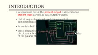
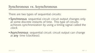
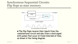
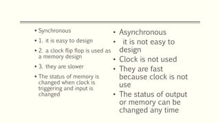
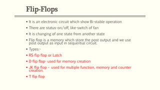
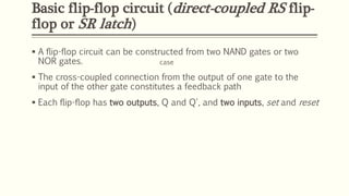
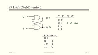
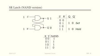
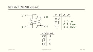
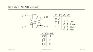
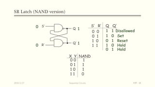
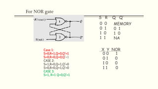
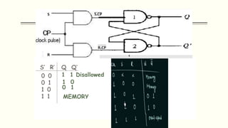
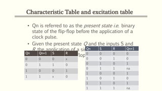
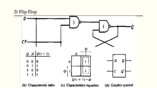
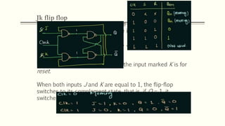
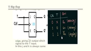
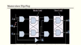
Er. Nawaraj Bhandari
Digital Logic
Chapter 6:
Sequential Logic
INTRODUCTION
 In sequential circuit the present output is depend upon
present input as well as past output/outputs.
 Half of sequential circuit used the concept of
combinational circuit
 Its contain both flip flop and counter.
 Block diagram shows external outputs in a sequential
circuit are a function not only of external inputs, but also
of the present state of the memory elements
Synchronous vs. Asynchronous
There are two types of sequential circuits:
 Synchronous sequential circuit: circuit output changes only
at some discrete instants of time. This type of circuits
achieves synchronization by using a timing signal called the
clock.
 Asynchronous sequential circuit: circuit output can change
at any time (clockless).
2019/2/27 Sequential Circuits PJF - 3
Synchronous Sequential Circuits:
Flip flops as state memory
2019/2/27 Sequential Circuits PJF - 4
 The flip-flops receive their inputs from the
combinational circuit and also from a clock signal
with pulses that occur at fixed intervals of time,
as shown in the timing diagram.
 Synchronous
 1. it is easy to design
 2. a clock flip flop is used as
a memory design
 3. they are slower
 The status of memory is
changed when clock is
triggering and input is
changed
• Asynchronous
• it is not easy to
design
• Clock is not used
• They are fast
because clock is not
use
• The status of output
or memory can be
changed any time
Flip-Flops
 It is an electronic circuit which show Bi-stable operation
 There are status-on/off, like-switch of fan
 It is changing of one state from another state
 Flip flop is a memory which store the post output and we use
post output as input in sequential circuit.
 Types:-
 RS flip flop or Latch
 D flip flop- used for memory creation
 JK flip flop – used for multiple function, memory and counter
creation.
 T flip flop
Basic flip-flop circuit (direct-coupled RS flip-
flop or SR latch)
 A flip-flop circuit can be constructed from two NAND gates or two
NOR gates.
 The cross-coupled connection from the output of one gate to the
input of the other gate constitutes a feedback path
 Each flip-flop has two outputs, Q and Q', and two inputs, set and reset
case
SR Latch (NAND version)
2019/2/27 Sequential Circuits PJF - 8
S’
R’
Q
Q’
0 0
0 1
1 0
1 1
S’ R’ Q Q’0
1
1
0
1 0 Set
0 0 1
0 1 1
1 0 1
1 1 0
X Y NAND
SR Latch (NAND version)
2019/2/27 Sequential Circuits PJF - 9
S’
R’
Q
Q’
0 0
0 1
1 0
1 1
S’ R’ Q Q’1
1
1
0
1 0 Hold
0 0 1
0 1 1
1 0 1
1 1 0
X Y NAND
1 0 Set
SR Latch (NAND version)
2019/2/27 Sequential Circuits PJF - 10
S’
R’
Q
Q’
0 0
0 1
1 0
1 1
S’ R’ Q Q’1
0
0
1
0 0 1
0 1 1
1 0 1
1 1 0
X Y NAND
1 0 Hold
1 0 Set
0 1 Reset
SR Latch (NAND version)
2019/2/27 Sequential Circuits PJF - 11
S’
R’
Q
Q’
0 0
0 1
1 0
1 1
S’ R’ Q Q’1
1
0
1
0 0 1
0 1 1
1 0 1
1 1 0
X Y NAND
0 1 Hold
1 0 Set
0 1 Reset
1 0 Hold
SR Latch (NAND version)
2019/2/27 Sequential Circuits PJF - 12
S’
R’
Q
Q’
0
0
1
1
0 0 1
0 1 1
1 0 1
1 1 0
X Y NAND
0 1 Hold
0 1 Reset
0 0
0 1
1 0
1 1
S’ R’ Q Q’
1 0 Set
1 0 Hold
1 1 Disallowed
For NOR gate
Case 1:
S=0,R=1,Q=0,Q’=1
S=0,R=0,Q=0,Q’=1
CASE 2:
S=1,R=0,Q=1,Q’=0
S=0,R=0,Q=1,Q’=0
CASE 3:
S=1, R=1 Q=0,Q’=1
0 0
0 1
1 0
1 1
S R Q Q’
MEMORY
0 1
1 0
NA
0 0 1
0 1 0
1 0 0
1 1 0
X Y NOR
RS Flip-Flop
It consists of a basic flip-flop circuit and two
additional NAND gates along with clock pulse
(CP) input. The pulse input acts as an enable
signal for the other two inputs.
When the pulse input goes to 1, information from
the S or R input is allowed to reach the output.
Set state: S = 1, R = 0, and CP = 1.
Reset state: S = 0, R = 1, and CP = 1.
In either case, when CP returns to 0, the circuit
remains in its previous state. When CP = 1 and
both the S and R inputs are equal to 0, the state
of the circuit does not change.
0 0
0 1
1 0
1 1
S’ R’ Q Q’
0 1
1 0
1 1 Disallowed
MEMORY
Characteristic Table and excitation table
• Qn is referred to as the present state i.e. binary
state of the flip-flop before the application of a
clock pulse.
• Given the present state Q and the inputs S and
R, the application of a single pulse in the CP
input causes the flip-flop to go to the next
state, Qn + 1.
CK S R Qn+1
0 x x Qn
1 0 0 Qn
1 0 1 0
1 1 0 1
1 1 1 na
Qn S R Qn+1
0 0 0 0
0 0 1 0
0 1 0 1
0 1 1 na
1 0 0 1
1 0 1 0
1 1 0 1
1 1 1 na
Qn Qn+1 S R
0 0 0 x
0 1 1 0
1 0 0 1
1 1 x 0
D Flip-Flop
• One way to eliminate the undesirable condition of the
indeterminate state in the RS flip-flop is to ensure that
inputs S and R are never equal to 1 at the same time.
• The D flip-flop has only two inputs: D and CP.
• The D input goes directly to the S input and its
complement is applied to the R input.
• As long as CP is 0, the outputs of gates 3 and 4 are at the
1 level and the circuit cannot change state regardless of
the value of D. The D input is sampled when CP = 1.
• If D is 1, the Q output goes to 1, placing the circuit in the
set state.
• If D is 0, output Q goes to 0 and the circuit switches to the
clear state
• In every state D is equal to output
Jk flip flop
A JK flip-flop is a refinement of the RS flip-flop in that the
indeterminate state of the RS type is defined in the JK type.
Inputs J and K behave like inputs S and R to set and clear
the flip-flop, respectively.
The input marked J is for set and the input marked K is for
reset.
When both inputs J and K are equal to 1, the flip-flop
switches to its complement state, that is, if Q = 1, it
switches to Q = 0, and vice versa.
T flip flop
The T or "toggle" flip-flop changes its output on each
clock edge, giving an output which is half the frequency of
the signal to the T input.
It is useful for constructing binary counters, frequency
dividers, and general binary addition devices.
It can be made from a J-K flip-flop by tying both of its
inputs high.
The T or "toggle" flip-flopchanges its output on eachclock
edge, giving an output which is half the frequency of the
signal to the T input.
In this j and k is always same
Master-slave Flip-Flop
The Master-Slave Flip-Flop is basically two gated SR flip-
flops connected together in a series configuration with
the slave having an inverted clock pulse.
The outputs from Q and Q from the “Slave” flip-flop are
fed back to the inputs of the “Master” with the outputs of
the “Master” flip flop being connected to the two inputs of
the “Slave” flip flop.
This feedback configuration from the slave’s output to the
master’s input gives the characteristic toggle of the JK flip
flop
When the clock is “LOW”, the outputs from the “master”
flip flop are latched and any additional changes to its
inputs are ignored. The gated “slave” flip flop now
Analysis of clock using D flip flop
Step 1
Calculate DA,DB,Y
DA=QA.X+QB
DB=QB.QA’
Y=X’QB’+X.QA
STEP 2
MAKE STATE TABLE
QA+=DA
QB+=DB
QA QB X QA+ QB+ Y
0 0 0 0 0 1
0 0 1 0 0 0
0 1 0 1 1 0
0 1 1 1 1 0
1 0 0 0 0 1
1 0 1 1 0 1
1 1 0 1 0 0
1 1 1 1 0 1
STATE DIAGRAM

Chapter 6: Sequential Logic

  • 1.
    Er. Nawaraj Bhandari DigitalLogic Chapter 6: Sequential Logic
  • 2.
    INTRODUCTION  In sequentialcircuit the present output is depend upon present input as well as past output/outputs.  Half of sequential circuit used the concept of combinational circuit  Its contain both flip flop and counter.  Block diagram shows external outputs in a sequential circuit are a function not only of external inputs, but also of the present state of the memory elements
  • 3.
    Synchronous vs. Asynchronous Thereare two types of sequential circuits:  Synchronous sequential circuit: circuit output changes only at some discrete instants of time. This type of circuits achieves synchronization by using a timing signal called the clock.  Asynchronous sequential circuit: circuit output can change at any time (clockless). 2019/2/27 Sequential Circuits PJF - 3
  • 4.
    Synchronous Sequential Circuits: Flipflops as state memory 2019/2/27 Sequential Circuits PJF - 4  The flip-flops receive their inputs from the combinational circuit and also from a clock signal with pulses that occur at fixed intervals of time, as shown in the timing diagram.
  • 5.
     Synchronous  1.it is easy to design  2. a clock flip flop is used as a memory design  3. they are slower  The status of memory is changed when clock is triggering and input is changed • Asynchronous • it is not easy to design • Clock is not used • They are fast because clock is not use • The status of output or memory can be changed any time
  • 6.
    Flip-Flops  It isan electronic circuit which show Bi-stable operation  There are status-on/off, like-switch of fan  It is changing of one state from another state  Flip flop is a memory which store the post output and we use post output as input in sequential circuit.  Types:-  RS flip flop or Latch  D flip flop- used for memory creation  JK flip flop – used for multiple function, memory and counter creation.  T flip flop
  • 7.
    Basic flip-flop circuit(direct-coupled RS flip- flop or SR latch)  A flip-flop circuit can be constructed from two NAND gates or two NOR gates.  The cross-coupled connection from the output of one gate to the input of the other gate constitutes a feedback path  Each flip-flop has two outputs, Q and Q', and two inputs, set and reset case
  • 8.
    SR Latch (NANDversion) 2019/2/27 Sequential Circuits PJF - 8 S’ R’ Q Q’ 0 0 0 1 1 0 1 1 S’ R’ Q Q’0 1 1 0 1 0 Set 0 0 1 0 1 1 1 0 1 1 1 0 X Y NAND
  • 9.
    SR Latch (NANDversion) 2019/2/27 Sequential Circuits PJF - 9 S’ R’ Q Q’ 0 0 0 1 1 0 1 1 S’ R’ Q Q’1 1 1 0 1 0 Hold 0 0 1 0 1 1 1 0 1 1 1 0 X Y NAND 1 0 Set
  • 10.
    SR Latch (NANDversion) 2019/2/27 Sequential Circuits PJF - 10 S’ R’ Q Q’ 0 0 0 1 1 0 1 1 S’ R’ Q Q’1 0 0 1 0 0 1 0 1 1 1 0 1 1 1 0 X Y NAND 1 0 Hold 1 0 Set 0 1 Reset
  • 11.
    SR Latch (NANDversion) 2019/2/27 Sequential Circuits PJF - 11 S’ R’ Q Q’ 0 0 0 1 1 0 1 1 S’ R’ Q Q’1 1 0 1 0 0 1 0 1 1 1 0 1 1 1 0 X Y NAND 0 1 Hold 1 0 Set 0 1 Reset 1 0 Hold
  • 12.
    SR Latch (NANDversion) 2019/2/27 Sequential Circuits PJF - 12 S’ R’ Q Q’ 0 0 1 1 0 0 1 0 1 1 1 0 1 1 1 0 X Y NAND 0 1 Hold 0 1 Reset 0 0 0 1 1 0 1 1 S’ R’ Q Q’ 1 0 Set 1 0 Hold 1 1 Disallowed
  • 13.
    For NOR gate Case1: S=0,R=1,Q=0,Q’=1 S=0,R=0,Q=0,Q’=1 CASE 2: S=1,R=0,Q=1,Q’=0 S=0,R=0,Q=1,Q’=0 CASE 3: S=1, R=1 Q=0,Q’=1 0 0 0 1 1 0 1 1 S R Q Q’ MEMORY 0 1 1 0 NA 0 0 1 0 1 0 1 0 0 1 1 0 X Y NOR
  • 14.
    RS Flip-Flop It consistsof a basic flip-flop circuit and two additional NAND gates along with clock pulse (CP) input. The pulse input acts as an enable signal for the other two inputs. When the pulse input goes to 1, information from the S or R input is allowed to reach the output. Set state: S = 1, R = 0, and CP = 1. Reset state: S = 0, R = 1, and CP = 1. In either case, when CP returns to 0, the circuit remains in its previous state. When CP = 1 and both the S and R inputs are equal to 0, the state of the circuit does not change. 0 0 0 1 1 0 1 1 S’ R’ Q Q’ 0 1 1 0 1 1 Disallowed MEMORY
  • 15.
    Characteristic Table andexcitation table • Qn is referred to as the present state i.e. binary state of the flip-flop before the application of a clock pulse. • Given the present state Q and the inputs S and R, the application of a single pulse in the CP input causes the flip-flop to go to the next state, Qn + 1. CK S R Qn+1 0 x x Qn 1 0 0 Qn 1 0 1 0 1 1 0 1 1 1 1 na Qn S R Qn+1 0 0 0 0 0 0 1 0 0 1 0 1 0 1 1 na 1 0 0 1 1 0 1 0 1 1 0 1 1 1 1 na Qn Qn+1 S R 0 0 0 x 0 1 1 0 1 0 0 1 1 1 x 0
  • 16.
    D Flip-Flop • Oneway to eliminate the undesirable condition of the indeterminate state in the RS flip-flop is to ensure that inputs S and R are never equal to 1 at the same time. • The D flip-flop has only two inputs: D and CP. • The D input goes directly to the S input and its complement is applied to the R input. • As long as CP is 0, the outputs of gates 3 and 4 are at the 1 level and the circuit cannot change state regardless of the value of D. The D input is sampled when CP = 1. • If D is 1, the Q output goes to 1, placing the circuit in the set state. • If D is 0, output Q goes to 0 and the circuit switches to the clear state • In every state D is equal to output
  • 17.
    Jk flip flop AJK flip-flop is a refinement of the RS flip-flop in that the indeterminate state of the RS type is defined in the JK type. Inputs J and K behave like inputs S and R to set and clear the flip-flop, respectively. The input marked J is for set and the input marked K is for reset. When both inputs J and K are equal to 1, the flip-flop switches to its complement state, that is, if Q = 1, it switches to Q = 0, and vice versa.
  • 18.
    T flip flop TheT or "toggle" flip-flop changes its output on each clock edge, giving an output which is half the frequency of the signal to the T input. It is useful for constructing binary counters, frequency dividers, and general binary addition devices. It can be made from a J-K flip-flop by tying both of its inputs high. The T or "toggle" flip-flopchanges its output on eachclock edge, giving an output which is half the frequency of the signal to the T input. In this j and k is always same
  • 19.
    Master-slave Flip-Flop The Master-SlaveFlip-Flop is basically two gated SR flip- flops connected together in a series configuration with the slave having an inverted clock pulse. The outputs from Q and Q from the “Slave” flip-flop are fed back to the inputs of the “Master” with the outputs of the “Master” flip flop being connected to the two inputs of the “Slave” flip flop. This feedback configuration from the slave’s output to the master’s input gives the characteristic toggle of the JK flip flop When the clock is “LOW”, the outputs from the “master” flip flop are latched and any additional changes to its inputs are ignored. The gated “slave” flip flop now
  • 20.
    Analysis of clockusing D flip flop Step 1 Calculate DA,DB,Y DA=QA.X+QB DB=QB.QA’ Y=X’QB’+X.QA STEP 2 MAKE STATE TABLE QA+=DA QB+=DB QA QB X QA+ QB+ Y 0 0 0 0 0 1 0 0 1 0 0 0 0 1 0 1 1 0 0 1 1 1 1 0 1 0 0 0 0 1 1 0 1 1 0 1 1 1 0 1 0 0 1 1 1 1 0 1
  • 21.

Editor's Notes