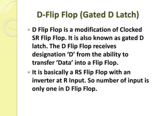
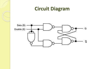
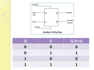
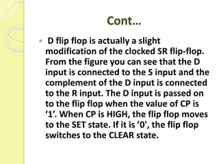
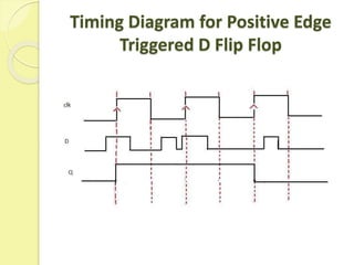
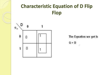
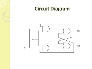
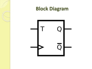
Name: Panchal Dhrumil Indravadan
Subject: Digital electronics
Branch: Computer Engineering (B.E.)
Semester: THIRD Sem
Year: 2018-19
WELCOME
TOPIC
Design of T flip flop and D flip flop
CONTAIN
 D Flip Flop
 T Flip Flop
D-Flip Flop (Gated D Latch)
 D Flip Flop is a modification of Clocked
SR Flip Flop. It is also known as gated D
latch. The D Flip Flop receives
designation ‘D’ from the ability to
transfer ‘Data’ into a Flip Flop.
 It is basically a RS Flip Flop with an
inverter at R Input. So number of input is
only one in D Flip Flop.
Circuit Diagram
Q D Q (t+1)
0 0 0
0 1 1
1 0 0
1 1 1
D Flip Flop Gated D Latch using
NOR Gate
Cont…
 D flip flop is actually a slight
modification of the clocked SR flip-flop.
From the figure you can see that the D
input is connected to the S input and the
complement of the D input is connected
to the R input. The D input is passed on
to the flip flop when the value of CP is
‘1’. When CP is HIGH, the flip flop moves
to the SET state. If it is ’0', the flip flop
switches to the CLEAR state.
Timing Diagram
Timing Diagram for Positive Edge
Triggered D Flip Flop
Characteristic Equation of D Flip
Flop
T-Flip Flop: Toggle Flip Flop
 T flip-flops are similar to JK flip-flops. T
flip-flops are single input version of JK flip-
flops. This modified form of JK flip-flop is
obtained by connecting both inputs J and
K together. This flip flop has only one
input along with Clock pulse. These flip-
flops are called T flip-flops because of
their ability to complement its state (i.e.)
Toggle. So they are called as Toggle flip-
flop.
 When J=K=0, then T=0
If CP=1 the output is same as previous
state. It is Memory state of Flip Flop.
Cont…
 When J=K=1, then T=1
If Clock pulse is high (CP=1) then, the
output begins to toggle. So, for a
previous value of Q = 1, it switches to
Q=0 and for a previous value of Q = 0, it
switches to Q=1.
 Here also the restriction on the pulse
width can be eliminated with a master-
slave or edge triggered construction.
Take a look at the circuit and truth table
given for T Flip Flop.
Circuit Diagram
Block Diagram
Characteristic Equation for T Flip
Flop
Q T Q (T+1)
0 0 0
0 1 1
1 0 1
1 1 0
From the truth table, characteristic equation
can be derived as follows:
References
 Inspiration from Asst. Prof. Purvik Rana
 Notes of DE
 Text book of DE
 Images from Google images
 Some our own knowledge
Thank You

D and T Flip Flop

  • 1.
    Name: Panchal DhrumilIndravadan Subject: Digital electronics Branch: Computer Engineering (B.E.) Semester: THIRD Sem Year: 2018-19 WELCOME
  • 2.
    TOPIC Design of Tflip flop and D flip flop
  • 3.
    CONTAIN  D FlipFlop  T Flip Flop
  • 4.
    D-Flip Flop (GatedD Latch)  D Flip Flop is a modification of Clocked SR Flip Flop. It is also known as gated D latch. The D Flip Flop receives designation ‘D’ from the ability to transfer ‘Data’ into a Flip Flop.  It is basically a RS Flip Flop with an inverter at R Input. So number of input is only one in D Flip Flop.
  • 5.
  • 6.
    Q D Q(t+1) 0 0 0 0 1 1 1 0 0 1 1 1
  • 7.
    D Flip FlopGated D Latch using NOR Gate
  • 8.
    Cont…  D flipflop is actually a slight modification of the clocked SR flip-flop. From the figure you can see that the D input is connected to the S input and the complement of the D input is connected to the R input. The D input is passed on to the flip flop when the value of CP is ‘1’. When CP is HIGH, the flip flop moves to the SET state. If it is ’0', the flip flop switches to the CLEAR state.
  • 9.
  • 10.
    Timing Diagram forPositive Edge Triggered D Flip Flop
  • 11.
  • 12.
    T-Flip Flop: ToggleFlip Flop  T flip-flops are similar to JK flip-flops. T flip-flops are single input version of JK flip- flops. This modified form of JK flip-flop is obtained by connecting both inputs J and K together. This flip flop has only one input along with Clock pulse. These flip- flops are called T flip-flops because of their ability to complement its state (i.e.) Toggle. So they are called as Toggle flip- flop.  When J=K=0, then T=0 If CP=1 the output is same as previous state. It is Memory state of Flip Flop.
  • 13.
    Cont…  When J=K=1,then T=1 If Clock pulse is high (CP=1) then, the output begins to toggle. So, for a previous value of Q = 1, it switches to Q=0 and for a previous value of Q = 0, it switches to Q=1.  Here also the restriction on the pulse width can be eliminated with a master- slave or edge triggered construction. Take a look at the circuit and truth table given for T Flip Flop.
  • 14.
  • 15.
  • 16.
    Characteristic Equation forT Flip Flop Q T Q (T+1) 0 0 0 0 1 1 1 0 1 1 1 0 From the truth table, characteristic equation can be derived as follows:
  • 17.
    References  Inspiration fromAsst. Prof. Purvik Rana  Notes of DE  Text book of DE  Images from Google images  Some our own knowledge
  • 18.