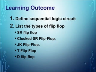
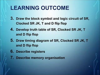
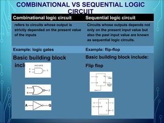
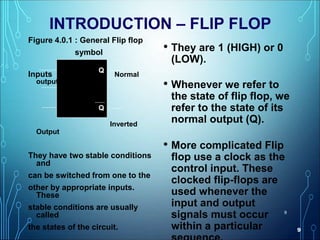
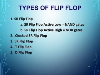
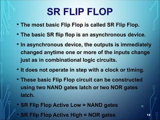
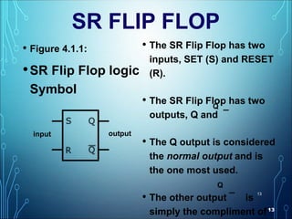
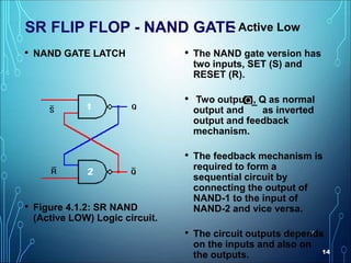
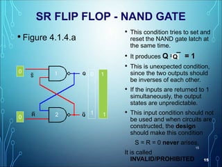
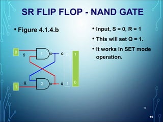
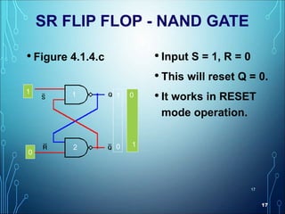
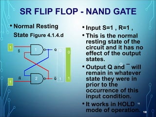
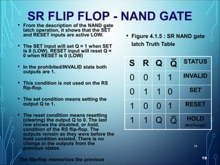
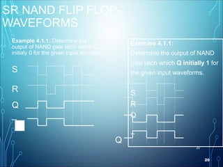
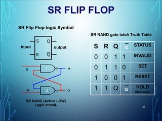
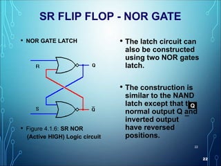
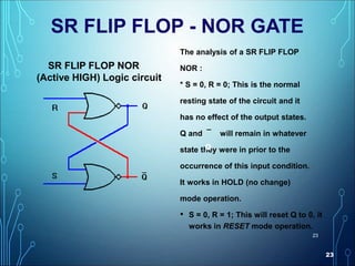
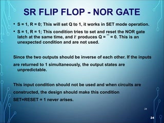
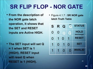
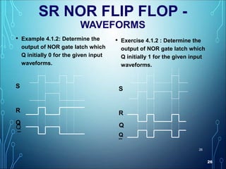
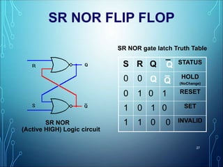
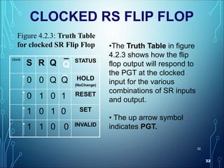
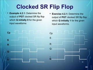
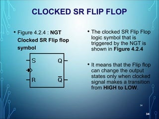
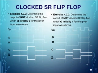
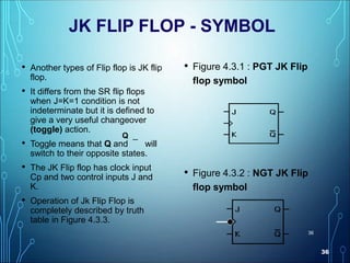
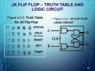
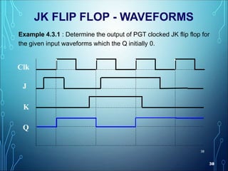
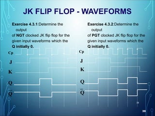
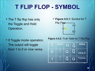
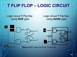
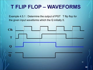
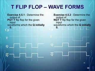
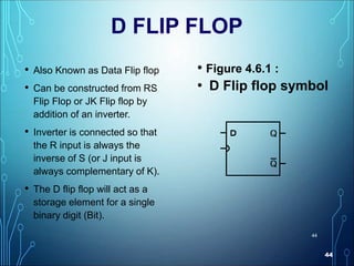
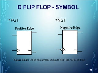
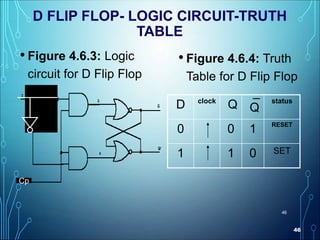
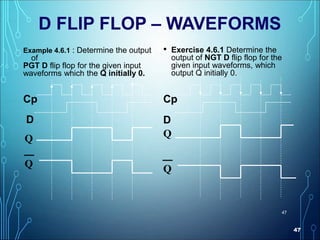
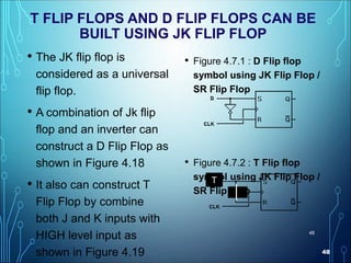
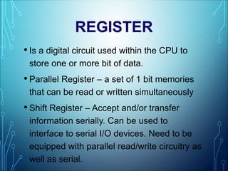
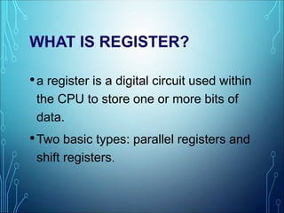
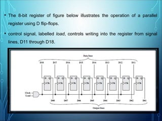
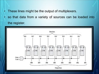
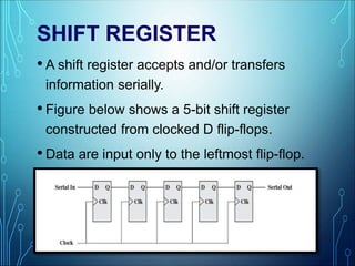
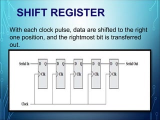
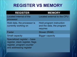
SlideShare a Scribd company logo
1
2.3 BUILD
SEQUENTIAL
LOGIC CIRCUIT
1
1. Define sequential logic circuit
2. List the types of flip flop
• SR flip flop
• Clocked SR Flip-Flop,
• JK Flip-Flop.
• T Flip-Flop
• D flip-flop
2
Learning Outcome
LEARNING OUTCOME
3. Draw the block symbol and logic circuit of SR,
Clocked SR JK, T and D flip flop
4. Develop truth table of SR, Clocked SR JK, T
and D flip flop
5. Draw timing diagram of SR, Clocked SR JK, T
and D flip flop
6. Describe registers
7. Describe memory organisation
3
SEQUENTIAL LOGIC CIRCUIT
• Define Sequential Circuits ?
• Sequential logic circuits is circuits is the type of a
digital system that does not only depend on current
input, but also the previous history of the system.
• For that reason sequential logic circuit require
memory to function.
• Sequential circuits have loops - these enable
circuits to receive feedback.
• The building block used to construct device that
store data is called Flip flop.
5
5
2.3SEQUENTIAL CIRCUITS
A general block diagram of a sequential
circuit
•The output of circuit depends on
the previous output and the present
inputs.
•The inputs must follow a specific
sequence to produce a required
output.
6
COMBINATION LOGIC CIRCUIT.
7
COMBINATIONAL VS SEQUENTIAL LOGIC
CIRCUIT
8
Combinational logic circuit Sequential logic circuit
refers to circuits whose output is
strictly depended on the present value
of the inputs
Circuits whose outputs depends not
only on the present input value but
also the past input value are known
as sequential logic circuits.
Example: logic gates Example: flip-flop
Basic building block
include:
Basic building block include:
Flip flop
9
9
INTRODUCTION – FLIP FLOP
• They are 1 (HIGH) or 0
(LOW).
• Whenever we refer to
the state of flip flop, we
refer to the state of its
normal output (Q).
• More complicated Flip
flop use a clock as the
control input. These
clocked flip-flops are
used whenever the
input and output
signals must occur
within a particular
Figure 4.0.1 : General Flip flop
symbol
Inputs Normal
output
Inverted
Output
They have two stable conditions
and
can be switched from one to the
other by appropriate inputs.
These
stable conditions are usually
called
the states of the circuit.
Q
Q
TYPES OF FLIP FLOP
1. SR Flip Flop
a. SR Flip Flop Active Low = NAND gates
b. SR Flip Flop Active High = NOR gates
2. Clocked SR Flip Flop
3. JK Flip Flop
4. T Flip Flop
5. D Flip Flop
10
THE USED OF FLIP FLOP
•For Memory circuits
•For Logic Control Devices
•For Counter Devices
•For Register Devices
11
12
12
SR FLIP FLOP
• The most basic Flip Flop is called SR Flip Flop.
• The basic SR flip flop is an asynchronous device.
• In asynchronous device, the outputs is immediately
changed anytime one or more of the inputs change
just as in combinational logic circuits.
• It does not operate in step with a clock or timing.
• These basic Flip Flop circuit can be constructed
using two NAND gates latch or two NOR gates
latch.
• SR Flip Flop Active Low = NAND gates
• SR Flip Flop Active High = NOR gates
13
13
SR FLIP FLOP
• Figure 4.1.1:
•SR Flip Flop logic
Symbol
• The SR Flip Flop has two
inputs, SET (S) and RESET
(R).
• The SR Flip Flop has two
outputs, Q and ¯
• The Q output is considered
the normal output and is
the one most used.
• The other output ¯ is
simply the compliment of
Q
Q
input output
14
14
SR FLIP FLOP - NAND GATE
• NAND GATE LATCH
• Figure 4.1.2: SR NAND
(Active LOW) Logic circuit.
• The NAND gate version has
two inputs, SET (S) and
RESET (R).
• Two outputs, Q as normal
output and ¯ as inverted
output and feedback
mechanism.
• The feedback mechanism is
required to form a
sequential circuit by
connecting the output of
NAND-1 to the input of
NAND-2 and vice versa.
• The circuit outputs depends
on the inputs and also on
the outputs.
Q
1
2
1
2
1
2
1
2
1
2
1
2
1
222
1
2
- Active Low
15
15
SR FLIP FLOP - NAND GATE
• Figure 4.1.4.a
• This condition tries to set and
reset the NAND gate latch at
the same time.
• It produces Q = ¯ = 1
• This is unexpected condition,
since the two outputs should
be inverses of each other.
• If the inputs are returned to 1
simultaneously, the output
states are unpredictable.
• This input condition should not
be used and when circuits are
constructed, the design
should make this condition
S = R = 0 never arises.
It is called
INVALID/PROHIBITED
0
0 1
1
1
0
Q
1
2
16
16
SR FLIP FLOP - NAND GATE
• Input, S = 0, R = 1
• This will set Q = 1.
• It works in SET mode
operation.
• Figure 4.1.4.b
0
1
0 1
01
1
2
17
17
SR FLIP FLOP - NAND GATE
• Figure 4.1.4.c • Input S = 1, R = 0
• This will reset Q = 0.
• It works in RESET
mode operation.
1
0
1
0
0
11
2
18
18
SR FLIP FLOP - NAND GATE
• Normal Resting
State Figure 4.1.4.d
• Input S=1 , R=1 ,
• This is the normal
resting state of the
circuit and it has no
effect of the output
states.
• Output Q and ¯ will
remain in whatever
state they were in
prior to the
occurrence of this
input condition.
• It works in HOLD
mode of operation.
0
1
1
1
0
1
1
1
1
1
11
1
000
1
Q
1
2
19
19
SR FLIP FLOP - NAND GATE
• From the description of the NAND gate
latch operation, it shows that the SET
and RESET inputs are active LOW.
• The SET input will set Q = 1 when SET
is 0 (LOW). RESET input will reset Q =
0 when RESET is 0 (LOW)
• In the prohibited/INVALID state both
outputs are 1.
• This condition is not used on the RS
flip-flop.
• The set condition means setting the
output Q to 1.
• The reset condition means resetting
(clearing) the output Q to 0. The last
row shows the disabled, or hold,
condition of the RS flip-flop. The
outputs remain as they were before the
hold condition existed. There is no
change in the outputs from the
previous states.
The flip-flop memorizes the previous
• Figure 4.1.5 : SR NAND gate
latch Truth Table
S R Q ¯ STATUS
0 0 1 1 INVALID
0 1 1 0 SET
1 0 0 1 RESET
1 1 Q ¯ HOLD
(NoChange)
Q
Q
20
20
SR NAND FLIP FLOP-
WAVEFORMS
Exercise 4.1.1:
Determine the output of NAND
gate latch which Q initially 1 for
the given input waveforms.
S
R
Q
¯
Example 4.1.1: Determine the
output of NAND gate latch which Q
initialy 0 for the given input waveform.
S
R
Q
¯Q
Q
SR FLIP FLOP
21
S R Q ¯ STATUS
0 0 1 1 INVALID
0 1 1 0 SET
1 0 0 1 RESET
1 1 Q ¯ HOLD
(NoChange)
SR NAND gate latch Truth Table
input output
1
2
SR NAND (Active LOW)
Logic circuit.
SR Flip Flop logic Symbol
Q
Q
22
22
SR FLIP FLOP - NOR GATE
• NOR GATE LATCH
• Figure 4.1.6: SR NOR
(Active HIGH) Logic circuit
• The latch circuit can
also be constructed
using two NOR gates
latch.
• The construction is
similar to the NAND
latch except that the
normal output Q and
inverted output ¯
have reversed
positions.
Q
23
23
SR FLIP FLOP - NOR GATE
The analysis of a SR FLIP FLOP
NOR :
* S = 0, R = 0; This is the normal
resting state of the circuit and it
has no effect of the output states.
Q and ¯ will remain in whatever
state they were in prior to the
occurrence of this input condition.
It works in HOLD (no change)
mode operation.
• S = 0, R = 1; This will reset Q to 0, it
works in RESET mode operation.
SR FLIP FLOP NOR
(Active HIGH) Logic circuit
Q
24
24
SR FLIP FLOP - NOR GATE
• S = 1, R = 0; This will set Q to 1, it works in SET mode operation.
• S = 1, R = 1; This condition tries to set and reset the NOR gate
latch at the same time, and it produces Q = ¯ = 0. This is an
unexpected condition and are not used.
Since the two outputs should be inverse of each other. If the inputs
are returned to 1 simultaneously, the output states are
unpredictable.
This input condition should not be used and when circuits are
constructed, the design should make this condition
SET=RESET = 1 never arises.
Q
25
25
SR FLIP FLOP - NOR GATE
• From the description of
the NOR gate latch
operation, it shows that
the SET and RESET
inputs are Active HIGH.
• The SET input will set Q
= 1 when SET is 1
(HIGH). RESET input
will reset Q when
RESET is 1 (HIGH).
• Figure 4.1.7 : SR NOR gate
latch Truth Table
S R Q ¯ STATUS
0 0 HOLD
(NoChange)
0 1 0 1 RESET
1 0 1 0 SET
1 1 0 0 INVALID
Q Q
Q
_
26
26
SR NOR FLIP FLOP -
WAVEFORMS
• Example 4.1.2: Determine the
output of NOR gate latch which
Q initially 0 for the given input
waveforms.
S
R
Q
¯
• Exercise 4.1.2 : Determine the
output of NOR gate latch which
Q initially 1 for the given input
waveforms.
S
R
Q
¯
Q
Q
SR NOR FLIP FLOP
27
S R Q ¯ STATUS
0 0 HOLD
(NoChange)
0 1 0 1 RESET
1 0 1 0 SET
1 1 0 0 INVALID
SR NOR gate latch Truth Table
SR NOR
(Active HIGH) Logic circuit
Q Q
_
Q
28
28
THE CLOCK
•In synchronous device, the exact
times at which any output can change
states are controlled by a signal
commonly called the clock.
•The clock signal is generally a
rectangular pulse train or a square
wave as shown in figure 4.9.
•The clock is distributed to all parts of
the system, and most of the system
outputs can change state only when
the clock makes a transition.
29
29
THE CLOCK
• When the clock changes from a LOW state to a HIGH
state, this is called the positive-going transition (PGT)
or positive edge triggered.
• When the clock changes from a HIGH state to a LOW
state, it is called negative going transition (NGT) or
negative edge triggered.
Figure 4.2.1: Clock Pulse-Train
(a) Positive going transition
(b) Negative going transition
Enable
Disable
30
30
CLOCKED SR FLIP FLOP
• Additional clock input is
added to change the SR
flip-flop from an element
used in asynchronous
sequential circuits to one,
which can be used in
synchronous circuits.
• The clocked SR flip flop
logic symbol that is
triggered by the PGT is
shown in Figure 4.2.2
• Its means that the flip flop
can change the output
states only when clock
signal makes a transition
• Figure 4.2.2 : PGT Clocked
SR Flip flop symbol
31
32
32
CLOCKED RS FLIP FLOP
clock
S R Q ¯ STATUS
0 0 Q Q HOLD
(NoChange)
0 1 0 1 RESET
1 0 1 0 SET
1 1 0 0 INVALID
Figure 4.2.3: Truth Table
for clocked SR Flip Flop •The Truth Table in figure
4.2.3 shows how the flip
flop output will respond to
the PGT at the clocked
input for the various
combinations of SR inputs
and output.
• The up arrow symbol
indicates PGT.
Q
_
33
33
• Example 4.2.1: Determine the
output of PGT clocked SR flip flop
which Q initially 0 for the given
input waveforms
Cp
S
R
Q
¯
• Exercise 4.2.1: Determine the
output of PGT clocked SR flip flop
which Q initially 1 for the given
input waveforms.
Cp
S
R
Q
¯
Clocked SR Flip Flop
Q Q
34
34
CLOCKED SR FLIP FLOP
• Figure 4.2.4 : NGT
Clocked SR Flip flop
symbol
• The clocked SR Flip Flop
logic symbol that is
triggered by the NGT is
shown in Figure 4.2.4
• It means that the Flip flop
can change the output
states only when clocked
signal makes a transition
from HIGH to LOW.
35
35
CLOCKED SR FLIP FLOP
• Example 4.2.2: Determine the
output of NGT clocked SR flip flop
which Q initially 0 for the given
input waveforms
Cp
S
R
Q
¯
• Exercise 4.2.2: Determine the
output of NGT clocked SR flip flop
which Q initially 1 for the given
input waveforms.
Cp
S
R
Q
¯
Q
Q
36
36
JK FLIP FLOP - SYMBOL
• Another types of Flip flop is JK flip
flop.
• It differs from the SR flip flops
when J=K=1 condition is not
indeterminate but it is defined to
give a very useful changeover
(toggle) action.
• Toggle means that Q and ¯ will
switch to their opposite states.
• The JK Flip flop has clock input
Cp and two control inputs J and
K.
• Operation of Jk Flip Flop is
completely described by truth
table in Figure 4.3.3.
• Figure 4.3.1 : PGT JK Flip
flop symbol
• Figure 4.3.2 : NGT JK Flip
flop symbol
Q
37
37
JK FLIP FLOP – TRUTH TABLE AND
LOGIC CIRCUIT
Figure 4.3.3: Truth Table
for JK Flip Flop
• Figure 4.3.4: JK FLIP FLOP
LOGIC CIRCUIT
clock
J K Q ¯ STATUS
0 0 HOLD
(No Change)
0 1 0 1 RESET
1 0 1 0 SET
1 1 Toggle
Q
Q
_
Q
Q Q
_
38
38
JK FLIP FLOP - WAVEFORMS
Example 4.3.1 : Determine the output of PGT clocked JK flip flop for
the given input waveforms which the Q initially 0.
J
Clk
K
Q
39
39
JK FLIP FLOP - WAVEFORMS
Exercise 4.3.1:Determine the
output
of NGT clocked JK flip flop for the
given input waveforms which the
Q initially 0.
Exercise 4.3.2:Determine the
output
of PGT clocked JK flip flop for the
given input waveforms which the
Q initially 0.
J
K
Q
Cp
¯Q
Cp Cp
K
J
Q
Q
¯
40
40
T FLIP FLOP - SYMBOL
• The T flip flop has only
the Toggle and Hold
Operation.
• If Toggle mode operation.
The output will toggle
from 1 to 0 or vice versa.
• Figure 4.5.1: Symbol for T
Flip Flop
T clock
Q status
0 Q Q HOLD
1 Q Q TOGOL
Q
Figure 4.5.2 :Truth Table for T Flip Flop
CP
T
41
41
T FLIP FLOP – LOGIC CIRCUIT
Cp
T
T
Logic circuit T Flip flop
using NOR gate
Logic circuit T Flip flop
using NAND gate
Figure 4.5.3: Logic circuit for T Flip Flop
42
42
T FLIP FLOP – WAVEFORMS
Example 4.5.1 : Determine the output of PGT T flip flop for
the given input waveforms which the Q initially 0.
T
Clk
Q
Q
43
43
T FLIP FLOP – WAVE FORMS
Exercise 4.5.1 : Determine the
output of
PGT T flip flop for the given
input
waveforms which the Q initially
0.
Exercise 4.5.2 : Determine the
output of
NGT T flip flop for the given
input
waveforms which the Q initially
0.
CpCp
Q
T
Q
Q
T
Q
44
44
D FLIP FLOP
• Also Known as Data Flip flop
• Can be constructed from RS
Flip Flop or JK Flip flop by
addition of an inverter.
• Inverter is connected so that
the R input is always the
inverse of S (or J input is
always complementary of K).
• The D flip flop will act as a
storage element for a single
binary digit (Bit).
• Figure 4.6.1 :
• D Flip flop symbol
45
45
D FLIP FLOP - SYMBOL
• PGT • NGT
D
Clk
Q
Q
D
Flip Flop
Positive Edge
D
Clk
Q
Q
D
Flip Flop
Negative Edge
Figure 4.6.2 : D Flip flop symbol using JK Flip Flop / SR Flip Flop
46
46
D FLIP FLOP- LOGIC CIRCUIT-TRUTH
TABLE
• Figure 4.6.3: Logic
circuit for D Flip Flop
• Figure 4.6.4: Truth
Table for D Flip Flop
D clock
Q ¯ status
0 0 1 RESET
1 1 0 SET
Q
Cp
47
47
D FLIP FLOP – WAVEFORMS
Example 4.6.1 : Determine the output
of
PGT D flip flop for the given input
waveforms which the Q initially 0.
Cp
D
• Exercise 4.6.1 Determine the
output of NGT D flip flop for the
given input waveforms, which
output Q initially 0.
Cp
D
Q
Q
Q
Q
48
48
T FLIP FLOPS AND D FLIP FLOPS CAN BE
BUILT USING JK FLIP FLOP
• The JK flip flop is
considered as a universal
flip flop.
• A combination of Jk flip
flop and an inverter can
construct a D Flip Flop as
shown in Figure 4.18
• It also can construct T
Flip Flop by combine
both J and K inputs with
HIGH level input as
shown in Figure 4.19
• Figure 4.7.1 : D Flip flop
symbol using JK Flip Flop /
SR Flip Flop
• Figure 4.7.2 : T Flip flop
symbol using JK Flip Flop /
SR Flip Flop
T
REGISTER
• Is a digital circuit used within the CPU to
store one or more bit of data.
• Parallel Register – a set of 1 bit memories
that can be read or written simultaneously
• Shift Register – Accept and/or transfer
information serially. Can be used to
interface to serial I/O devices. Need to be
equipped with parallel read/write circuitry as
well as serial.
WHAT IS REGISTER?
•a register is a digital circuit used within
the CPU to store one or more bits of
data.
•Two basic types: parallel registers and
shift registers.
PARALLEL REGISTERS
• consists of a set of 1-bit memories that can
be read or written simultaneously.
• It is used to store data.
• The 8-bit register of figure below illustrates the operation of a parallel
register using D flip-flops.
• control signal, labelled load, controls writing into the register from signal
lines, D11 through D18.
• These lines might be the output of multiplexers.
• so that data from a variety of sources can be loaded into
the register.
SHIFT REGISTER
• A shift register accepts and/or transfers
information serially.
• Figure below shows a 5-bit shift register
constructed from clocked D flip-flops.
• Data are input only to the leftmost flip-flop.
SHIFT REGISTER
With each clock pulse, data are shifted to the right
one position, and the rightmost bit is transferred
out.
CONT…
•Shift registers can be used to interface
to serial I/O devices.
•It can be used within the ALU to
perform logical shift and rotate
functions.
MEMORY ORGANISATION
57
PRIMARY STORAGE
• is the top level and is made up of CPU registers, CPU cache
and memory which are the only components that are directly
accessible to the systems CPU.
• The CPU can continuously read data stored in these areas
and execute all instructions as required quickly in a uniform
manner.
• Secondary Storage differs from primary storage in that it is not
directly accessible by the CPU.
• A system uses input/output (I/O) channels to connect to the
secondary storage which control the data flow through a
system when required and on request
58
SECONDARY STORAGE
• is non-volatile so does not lose data when it is powered
down so consequently modern computer systems tend
to have a more secondary storage than primary storage.
• All secondary storage today consist of hard disk drives
(HDD), usually set up in a RAID configuration, however
older installations also included removable media such
us magneto optical or MO
59
TERTIARY STORAGE
• is mainly used as backup and archival of data and
although based on the slowest devices can be
classed as the most important in terms of data
protection against a variety of disasters that can
affect an IT infrastructure.
• Most devices in this segment are automated via
robotics and software to reduce management costs
and risk of human error and consist primarily of disk
& tape based back up devices
60
OFFLINE STORAGE
• is the final category and is where removable
types of storage media sit such as tape
cartridges and optical disc such as CD and
DVD.
• is can be used to transfer data between
systems but also allow for data to be
secured offsite to ensure companies always
have a copy of valuable data in the event of
a disaster.
61
REGISTER VS MEMORY
REGISTER MEMORY
Located internal of the
processor
Located external to the CPU
Hold data, the processor is
currently working on
Hold program instruction
and the data, the program
requires
Faster Slower (RAM)
Small capacity Bigger capacity
Specialized register – base
register, stack register, flags
register, program counter
and addressing register

More Related Content

What's hot (20)

Presentation On Flip-Flop
Presentation On Flip-FlopPresentation On Flip-Flop
Presentation On Flip-Flop
 
flip flops
flip flops flip flops
flip flops
 
COUNTERS(Synchronous & Asynchronous)
COUNTERS(Synchronous & Asynchronous)COUNTERS(Synchronous & Asynchronous)
COUNTERS(Synchronous & Asynchronous)
 
Flip flop
Flip flopFlip flop
Flip flop
 
Flipflop
FlipflopFlipflop
Flipflop
 
latches
 latches latches
latches
 
flip flop circuits and its applications
flip flop circuits and its applicationsflip flop circuits and its applications
flip flop circuits and its applications
 
All flipflop
All flipflopAll flipflop
All flipflop
 
Flip Flop
Flip FlopFlip Flop
Flip Flop
 
Lecture 5 Synchronous Sequential Logic
Lecture 5 Synchronous Sequential LogicLecture 5 Synchronous Sequential Logic
Lecture 5 Synchronous Sequential Logic
 
Chapter 6: Sequential Logic
Chapter 6: Sequential LogicChapter 6: Sequential Logic
Chapter 6: Sequential Logic
 
D and T Flip Flop
D and T Flip FlopD and T Flip Flop
D and T Flip Flop
 
Latches & flip flop
Latches & flip flopLatches & flip flop
Latches & flip flop
 
Flip flop
Flip flopFlip flop
Flip flop
 
Latches and flip flops
Latches and flip flopsLatches and flip flops
Latches and flip flops
 
Flip flops, counters & registers
Flip flops, counters & registersFlip flops, counters & registers
Flip flops, counters & registers
 
Sequential Logic Circuit
Sequential Logic CircuitSequential Logic Circuit
Sequential Logic Circuit
 
SHIFT REGISTERS
SHIFT REGISTERSSHIFT REGISTERS
SHIFT REGISTERS
 
Digital Registers & Counters
Digital Registers & CountersDigital Registers & Counters
Digital Registers & Counters
 
Flip flop
Flip flopFlip flop
Flip flop
 

Similar to Sequential circuit

Sequential logic circuits flip-flop pt 1
Sequential logic circuits   flip-flop pt 1Sequential logic circuits   flip-flop pt 1
Sequential logic circuits flip-flop pt 1Sarah Sue Calbio
 
Digital Electronics Unit_3.pptx
Digital Electronics Unit_3.pptxDigital Electronics Unit_3.pptx
Digital Electronics Unit_3.pptxThapar Institute
 
Chapter 4 flip flop for students
Chapter 4 flip flop for studentsChapter 4 flip flop for students
Chapter 4 flip flop for studentsCT Sabariah Salihin
 
SEQUENTIAL LOGIC CIRCUITS (FLIP FLOPS AND LATCHES)
SEQUENTIAL LOGIC CIRCUITS (FLIP FLOPS AND LATCHES)SEQUENTIAL LOGIC CIRCUITS (FLIP FLOPS AND LATCHES)
SEQUENTIAL LOGIC CIRCUITS (FLIP FLOPS AND LATCHES)Sairam Adithya
 
Introduction to Sequential DevicesChapter 66.1 M.docx
Introduction to Sequential DevicesChapter 66.1 M.docxIntroduction to Sequential DevicesChapter 66.1 M.docx
Introduction to Sequential DevicesChapter 66.1 M.docxbagotjesusa
 
SEQUENTIAL CIRCUITS [FLIP FLOPS AND LATCHES]
SEQUENTIAL CIRCUITS [FLIP FLOPS AND LATCHES]SEQUENTIAL CIRCUITS [FLIP FLOPS AND LATCHES]
SEQUENTIAL CIRCUITS [FLIP FLOPS AND LATCHES]SUBHA SHREE
 
Sequential cmos logic circuits
Sequential cmos logic circuitsSequential cmos logic circuits
Sequential cmos logic circuitsSakshi Bhargava
 
Dee2034 chapter 4 flip flop for students part
Dee2034 chapter 4 flip flop  for students partDee2034 chapter 4 flip flop  for students part
Dee2034 chapter 4 flip flop for students partSITI SABARIAH SALIHIN
 
Latch and Flipflop.pptx
Latch and Flipflop.pptxLatch and Flipflop.pptx
Latch and Flipflop.pptxramkumarraja7
 
UNIT - III.pptx
UNIT - III.pptxUNIT - III.pptx
UNIT - III.pptxamudhak10
 
Digital_Electronics_Module_4_Sequential_Circuits v0.6.pptx
Digital_Electronics_Module_4_Sequential_Circuits v0.6.pptxDigital_Electronics_Module_4_Sequential_Circuits v0.6.pptx
Digital_Electronics_Module_4_Sequential_Circuits v0.6.pptxUtsavDas21
 
14827 unit 4_clocked_flip_flops
14827 unit 4_clocked_flip_flops14827 unit 4_clocked_flip_flops
14827 unit 4_clocked_flip_flopsSandeep Kumar
 
Digital design slides for engineering
Digital  design   slides for engineeringDigital  design   slides for engineering
Digital design slides for engineeringkasheen2803
 
9flipflopsupdated-191016140658.pptx
9flipflopsupdated-191016140658.pptx9flipflopsupdated-191016140658.pptx
9flipflopsupdated-191016140658.pptxudhayaveenaa
 
Flip Flop | Counters & Registers | Computer Fundamental and Organization
Flip Flop | Counters & Registers | Computer Fundamental and OrganizationFlip Flop | Counters & Registers | Computer Fundamental and Organization
Flip Flop | Counters & Registers | Computer Fundamental and OrganizationSmit Luvani
 

Similar to Sequential circuit (20)

Sequential logic circuits flip-flop pt 1
Sequential logic circuits   flip-flop pt 1Sequential logic circuits   flip-flop pt 1
Sequential logic circuits flip-flop pt 1
 
Lecture 1 6844
Lecture 1 6844Lecture 1 6844
Lecture 1 6844
 
Digital Electronics Unit_3.pptx
Digital Electronics Unit_3.pptxDigital Electronics Unit_3.pptx
Digital Electronics Unit_3.pptx
 
Chapter 4 flip flop for students
Chapter 4 flip flop for studentsChapter 4 flip flop for students
Chapter 4 flip flop for students
 
SEQUENTIAL LOGIC CIRCUITS (FLIP FLOPS AND LATCHES)
SEQUENTIAL LOGIC CIRCUITS (FLIP FLOPS AND LATCHES)SEQUENTIAL LOGIC CIRCUITS (FLIP FLOPS AND LATCHES)
SEQUENTIAL LOGIC CIRCUITS (FLIP FLOPS AND LATCHES)
 
Introduction to Sequential DevicesChapter 66.1 M.docx
Introduction to Sequential DevicesChapter 66.1 M.docxIntroduction to Sequential DevicesChapter 66.1 M.docx
Introduction to Sequential DevicesChapter 66.1 M.docx
 
SEQUENTIAL CIRCUITS [Flip-flops and Latches]
SEQUENTIAL CIRCUITS [Flip-flops and Latches]SEQUENTIAL CIRCUITS [Flip-flops and Latches]
SEQUENTIAL CIRCUITS [Flip-flops and Latches]
 
SEQUENTIAL CIRCUITS [FLIP FLOPS AND LATCHES]
SEQUENTIAL CIRCUITS [FLIP FLOPS AND LATCHES]SEQUENTIAL CIRCUITS [FLIP FLOPS AND LATCHES]
SEQUENTIAL CIRCUITS [FLIP FLOPS AND LATCHES]
 
Sequential cmos logic circuits
Sequential cmos logic circuitsSequential cmos logic circuits
Sequential cmos logic circuits
 
Dee2034 chapter 4 flip flop for students part
Dee2034 chapter 4 flip flop  for students partDee2034 chapter 4 flip flop  for students part
Dee2034 chapter 4 flip flop for students part
 
Latch and Flipflop.pptx
Latch and Flipflop.pptxLatch and Flipflop.pptx
Latch and Flipflop.pptx
 
UNIT - III.pptx
UNIT - III.pptxUNIT - III.pptx
UNIT - III.pptx
 
Digital_Electronics_Module_4_Sequential_Circuits v0.6.pptx
Digital_Electronics_Module_4_Sequential_Circuits v0.6.pptxDigital_Electronics_Module_4_Sequential_Circuits v0.6.pptx
Digital_Electronics_Module_4_Sequential_Circuits v0.6.pptx
 
14827 unit 4_clocked_flip_flops
14827 unit 4_clocked_flip_flops14827 unit 4_clocked_flip_flops
14827 unit 4_clocked_flip_flops
 
Digital design slides for engineering
Digital  design   slides for engineeringDigital  design   slides for engineering
Digital design slides for engineering
 
latchesflip-flop DLD
latchesflip-flop DLDlatchesflip-flop DLD
latchesflip-flop DLD
 
9flipflopsupdated-191016140658.pptx
9flipflopsupdated-191016140658.pptx9flipflopsupdated-191016140658.pptx
9flipflopsupdated-191016140658.pptx
 
Flip Flop | Counters & Registers | Computer Fundamental and Organization
Flip Flop | Counters & Registers | Computer Fundamental and OrganizationFlip Flop | Counters & Registers | Computer Fundamental and Organization
Flip Flop | Counters & Registers | Computer Fundamental and Organization
 
Flip flops
Flip flopsFlip flops
Flip flops
 
Unit IV version I.ppt
Unit IV version I.pptUnit IV version I.ppt
Unit IV version I.ppt
 

More from Brenda Debra

Central Processing Unit
Central Processing UnitCentral Processing Unit
Central Processing UnitBrenda Debra
 
Instruction Set and Assembly Language Programming
Instruction Set and Assembly Language ProgrammingInstruction Set and Assembly Language Programming
Instruction Set and Assembly Language ProgrammingBrenda Debra
 
Describe the register
Describe the registerDescribe the register
Describe the registerBrenda Debra
 
perform operation with boolean algebra
perform operation with boolean algebraperform operation with boolean algebra
perform operation with boolean algebraBrenda Debra
 
Understand data representation on CPU 1
Understand data representation on CPU 1Understand data representation on CPU 1
Understand data representation on CPU 1Brenda Debra
 
Computer System Architecture
Computer System ArchitectureComputer System Architecture
Computer System ArchitectureBrenda Debra
 

More from Brenda Debra (6)

Central Processing Unit
Central Processing UnitCentral Processing Unit
Central Processing Unit
 
Instruction Set and Assembly Language Programming
Instruction Set and Assembly Language ProgrammingInstruction Set and Assembly Language Programming
Instruction Set and Assembly Language Programming
 
Describe the register
Describe the registerDescribe the register
Describe the register
 
perform operation with boolean algebra
perform operation with boolean algebraperform operation with boolean algebra
perform operation with boolean algebra
 
Understand data representation on CPU 1
Understand data representation on CPU 1Understand data representation on CPU 1
Understand data representation on CPU 1
 
Computer System Architecture
Computer System ArchitectureComputer System Architecture
Computer System Architecture
 

Recently uploaded

Matatag-Curriculum and the 21st Century Skills Presentation.pptx
Matatag-Curriculum and the 21st Century Skills Presentation.pptxMatatag-Curriculum and the 21st Century Skills Presentation.pptx
Matatag-Curriculum and the 21st Century Skills Presentation.pptxJenilouCasareno
 
Instructions for Submissions thorugh G- Classroom.pptx
Instructions for Submissions thorugh G- Classroom.pptxInstructions for Submissions thorugh G- Classroom.pptx
Instructions for Submissions thorugh G- Classroom.pptxJheel Barad
 
UNIT – IV_PCI Complaints: Complaints and evaluation of complaints, Handling o...
UNIT – IV_PCI Complaints: Complaints and evaluation of complaints, Handling o...UNIT – IV_PCI Complaints: Complaints and evaluation of complaints, Handling o...
UNIT – IV_PCI Complaints: Complaints and evaluation of complaints, Handling o...Sayali Powar
 
[GDSC YCCE] Build with AI Online Presentation
[GDSC YCCE] Build with AI Online Presentation[GDSC YCCE] Build with AI Online Presentation
[GDSC YCCE] Build with AI Online PresentationGDSCYCCE
 
The Benefits and Challenges of Open Educational Resources
The Benefits and Challenges of Open Educational ResourcesThe Benefits and Challenges of Open Educational Resources
The Benefits and Challenges of Open Educational Resourcesaileywriter
 
slides CapTechTalks Webinar May 2024 Alexander Perry.pptx
slides CapTechTalks Webinar May 2024 Alexander Perry.pptxslides CapTechTalks Webinar May 2024 Alexander Perry.pptx
slides CapTechTalks Webinar May 2024 Alexander Perry.pptxCapitolTechU
 
The Art Pastor's Guide to Sabbath | Steve Thomason
The Art Pastor's Guide to Sabbath | Steve ThomasonThe Art Pastor's Guide to Sabbath | Steve Thomason
The Art Pastor's Guide to Sabbath | Steve ThomasonSteve Thomason
 
Basic_QTL_Marker-assisted_Selection_Sourabh.ppt
Basic_QTL_Marker-assisted_Selection_Sourabh.pptBasic_QTL_Marker-assisted_Selection_Sourabh.ppt
Basic_QTL_Marker-assisted_Selection_Sourabh.pptSourabh Kumar
 
NLC-2024-Orientation-for-RO-SDO (1).pptx
NLC-2024-Orientation-for-RO-SDO (1).pptxNLC-2024-Orientation-for-RO-SDO (1).pptx
NLC-2024-Orientation-for-RO-SDO (1).pptxssuserbdd3e8
 
Industrial Training Report- AKTU Industrial Training Report
Industrial Training Report- AKTU Industrial Training ReportIndustrial Training Report- AKTU Industrial Training Report
Industrial Training Report- AKTU Industrial Training ReportAvinash Rai
 
Application of Matrices in real life. Presentation on application of matrices
Application of Matrices in real life. Presentation on application of matricesApplication of Matrices in real life. Presentation on application of matrices
Application of Matrices in real life. Presentation on application of matricesRased Khan
 
Gyanartha SciBizTech Quiz slideshare.pptx
Gyanartha SciBizTech Quiz slideshare.pptxGyanartha SciBizTech Quiz slideshare.pptx
Gyanartha SciBizTech Quiz slideshare.pptxShibin Azad
 
Synthetic Fiber Construction in lab .pptx
Synthetic Fiber Construction in lab .pptxSynthetic Fiber Construction in lab .pptx
Synthetic Fiber Construction in lab .pptxPavel ( NSTU)
 
Solid waste management & Types of Basic civil Engineering notes by DJ Sir.pptx
Solid waste management & Types of Basic civil Engineering notes by DJ Sir.pptxSolid waste management & Types of Basic civil Engineering notes by DJ Sir.pptx
Solid waste management & Types of Basic civil Engineering notes by DJ Sir.pptxDenish Jangid
 
Sectors of the Indian Economy - Class 10 Study Notes pdf
Sectors of the Indian Economy - Class 10 Study Notes pdfSectors of the Indian Economy - Class 10 Study Notes pdf
Sectors of the Indian Economy - Class 10 Study Notes pdfVivekanand Anglo Vedic Academy
 
Fish and Chips - have they had their chips
Fish and Chips - have they had their chipsFish and Chips - have they had their chips
Fish and Chips - have they had their chipsGeoBlogs
 
Home assignment II on Spectroscopy 2024 Answers.pdf
Home assignment II on Spectroscopy 2024 Answers.pdfHome assignment II on Spectroscopy 2024 Answers.pdf
Home assignment II on Spectroscopy 2024 Answers.pdfTamralipta Mahavidyalaya
 

Recently uploaded (20)

Matatag-Curriculum and the 21st Century Skills Presentation.pptx
Matatag-Curriculum and the 21st Century Skills Presentation.pptxMatatag-Curriculum and the 21st Century Skills Presentation.pptx
Matatag-Curriculum and the 21st Century Skills Presentation.pptx
 
Instructions for Submissions thorugh G- Classroom.pptx
Instructions for Submissions thorugh G- Classroom.pptxInstructions for Submissions thorugh G- Classroom.pptx
Instructions for Submissions thorugh G- Classroom.pptx
 
Introduction to Quality Improvement Essentials
Introduction to Quality Improvement EssentialsIntroduction to Quality Improvement Essentials
Introduction to Quality Improvement Essentials
 
UNIT – IV_PCI Complaints: Complaints and evaluation of complaints, Handling o...
UNIT – IV_PCI Complaints: Complaints and evaluation of complaints, Handling o...UNIT – IV_PCI Complaints: Complaints and evaluation of complaints, Handling o...
UNIT – IV_PCI Complaints: Complaints and evaluation of complaints, Handling o...
 
[GDSC YCCE] Build with AI Online Presentation
[GDSC YCCE] Build with AI Online Presentation[GDSC YCCE] Build with AI Online Presentation
[GDSC YCCE] Build with AI Online Presentation
 
NCERT Solutions Power Sharing Class 10 Notes pdf
NCERT Solutions Power Sharing Class 10 Notes pdfNCERT Solutions Power Sharing Class 10 Notes pdf
NCERT Solutions Power Sharing Class 10 Notes pdf
 
The Benefits and Challenges of Open Educational Resources
The Benefits and Challenges of Open Educational ResourcesThe Benefits and Challenges of Open Educational Resources
The Benefits and Challenges of Open Educational Resources
 
slides CapTechTalks Webinar May 2024 Alexander Perry.pptx
slides CapTechTalks Webinar May 2024 Alexander Perry.pptxslides CapTechTalks Webinar May 2024 Alexander Perry.pptx
slides CapTechTalks Webinar May 2024 Alexander Perry.pptx
 
The Art Pastor's Guide to Sabbath | Steve Thomason
The Art Pastor's Guide to Sabbath | Steve ThomasonThe Art Pastor's Guide to Sabbath | Steve Thomason
The Art Pastor's Guide to Sabbath | Steve Thomason
 
Basic_QTL_Marker-assisted_Selection_Sourabh.ppt
Basic_QTL_Marker-assisted_Selection_Sourabh.pptBasic_QTL_Marker-assisted_Selection_Sourabh.ppt
Basic_QTL_Marker-assisted_Selection_Sourabh.ppt
 
NLC-2024-Orientation-for-RO-SDO (1).pptx
NLC-2024-Orientation-for-RO-SDO (1).pptxNLC-2024-Orientation-for-RO-SDO (1).pptx
NLC-2024-Orientation-for-RO-SDO (1).pptx
 
B.ed spl. HI pdusu exam paper-2023-24.pdf
B.ed spl. HI pdusu exam paper-2023-24.pdfB.ed spl. HI pdusu exam paper-2023-24.pdf
B.ed spl. HI pdusu exam paper-2023-24.pdf
 
Industrial Training Report- AKTU Industrial Training Report
Industrial Training Report- AKTU Industrial Training ReportIndustrial Training Report- AKTU Industrial Training Report
Industrial Training Report- AKTU Industrial Training Report
 
Application of Matrices in real life. Presentation on application of matrices
Application of Matrices in real life. Presentation on application of matricesApplication of Matrices in real life. Presentation on application of matrices
Application of Matrices in real life. Presentation on application of matrices
 
Gyanartha SciBizTech Quiz slideshare.pptx
Gyanartha SciBizTech Quiz slideshare.pptxGyanartha SciBizTech Quiz slideshare.pptx
Gyanartha SciBizTech Quiz slideshare.pptx
 
Synthetic Fiber Construction in lab .pptx
Synthetic Fiber Construction in lab .pptxSynthetic Fiber Construction in lab .pptx
Synthetic Fiber Construction in lab .pptx
 
Solid waste management & Types of Basic civil Engineering notes by DJ Sir.pptx
Solid waste management & Types of Basic civil Engineering notes by DJ Sir.pptxSolid waste management & Types of Basic civil Engineering notes by DJ Sir.pptx
Solid waste management & Types of Basic civil Engineering notes by DJ Sir.pptx
 
Sectors of the Indian Economy - Class 10 Study Notes pdf
Sectors of the Indian Economy - Class 10 Study Notes pdfSectors of the Indian Economy - Class 10 Study Notes pdf
Sectors of the Indian Economy - Class 10 Study Notes pdf
 
Fish and Chips - have they had their chips
Fish and Chips - have they had their chipsFish and Chips - have they had their chips
Fish and Chips - have they had their chips
 
Home assignment II on Spectroscopy 2024 Answers.pdf
Home assignment II on Spectroscopy 2024 Answers.pdfHome assignment II on Spectroscopy 2024 Answers.pdf
Home assignment II on Spectroscopy 2024 Answers.pdf
 

Sequential circuit

  • 2. 1. Define sequential logic circuit 2. List the types of flip flop • SR flip flop • Clocked SR Flip-Flop, • JK Flip-Flop. • T Flip-Flop • D flip-flop 2 Learning Outcome
  • 3. LEARNING OUTCOME 3. Draw the block symbol and logic circuit of SR, Clocked SR JK, T and D flip flop 4. Develop truth table of SR, Clocked SR JK, T and D flip flop 5. Draw timing diagram of SR, Clocked SR JK, T and D flip flop 6. Describe registers 7. Describe memory organisation 3
  • 4. SEQUENTIAL LOGIC CIRCUIT • Define Sequential Circuits ? • Sequential logic circuits is circuits is the type of a digital system that does not only depend on current input, but also the previous history of the system. • For that reason sequential logic circuit require memory to function. • Sequential circuits have loops - these enable circuits to receive feedback. • The building block used to construct device that store data is called Flip flop.
  • 5. 5 5 2.3SEQUENTIAL CIRCUITS A general block diagram of a sequential circuit
  • 6. •The output of circuit depends on the previous output and the present inputs. •The inputs must follow a specific sequence to produce a required output. 6
  • 8. COMBINATIONAL VS SEQUENTIAL LOGIC CIRCUIT 8 Combinational logic circuit Sequential logic circuit refers to circuits whose output is strictly depended on the present value of the inputs Circuits whose outputs depends not only on the present input value but also the past input value are known as sequential logic circuits. Example: logic gates Example: flip-flop Basic building block include: Basic building block include: Flip flop
  • 9. 9 9 INTRODUCTION – FLIP FLOP • They are 1 (HIGH) or 0 (LOW). • Whenever we refer to the state of flip flop, we refer to the state of its normal output (Q). • More complicated Flip flop use a clock as the control input. These clocked flip-flops are used whenever the input and output signals must occur within a particular Figure 4.0.1 : General Flip flop symbol Inputs Normal output Inverted Output They have two stable conditions and can be switched from one to the other by appropriate inputs. These stable conditions are usually called the states of the circuit. Q Q
  • 10. TYPES OF FLIP FLOP 1. SR Flip Flop a. SR Flip Flop Active Low = NAND gates b. SR Flip Flop Active High = NOR gates 2. Clocked SR Flip Flop 3. JK Flip Flop 4. T Flip Flop 5. D Flip Flop 10
  • 11. THE USED OF FLIP FLOP •For Memory circuits •For Logic Control Devices •For Counter Devices •For Register Devices 11
  • 12. 12 12 SR FLIP FLOP • The most basic Flip Flop is called SR Flip Flop. • The basic SR flip flop is an asynchronous device. • In asynchronous device, the outputs is immediately changed anytime one or more of the inputs change just as in combinational logic circuits. • It does not operate in step with a clock or timing. • These basic Flip Flop circuit can be constructed using two NAND gates latch or two NOR gates latch. • SR Flip Flop Active Low = NAND gates • SR Flip Flop Active High = NOR gates
  • 13. 13 13 SR FLIP FLOP • Figure 4.1.1: •SR Flip Flop logic Symbol • The SR Flip Flop has two inputs, SET (S) and RESET (R). • The SR Flip Flop has two outputs, Q and ¯ • The Q output is considered the normal output and is the one most used. • The other output ¯ is simply the compliment of Q Q input output
  • 14. 14 14 SR FLIP FLOP - NAND GATE • NAND GATE LATCH • Figure 4.1.2: SR NAND (Active LOW) Logic circuit. • The NAND gate version has two inputs, SET (S) and RESET (R). • Two outputs, Q as normal output and ¯ as inverted output and feedback mechanism. • The feedback mechanism is required to form a sequential circuit by connecting the output of NAND-1 to the input of NAND-2 and vice versa. • The circuit outputs depends on the inputs and also on the outputs. Q 1 2 1 2 1 2 1 2 1 2 1 2 1 222 1 2 - Active Low
  • 15. 15 15 SR FLIP FLOP - NAND GATE • Figure 4.1.4.a • This condition tries to set and reset the NAND gate latch at the same time. • It produces Q = ¯ = 1 • This is unexpected condition, since the two outputs should be inverses of each other. • If the inputs are returned to 1 simultaneously, the output states are unpredictable. • This input condition should not be used and when circuits are constructed, the design should make this condition S = R = 0 never arises. It is called INVALID/PROHIBITED 0 0 1 1 1 0 Q 1 2
  • 16. 16 16 SR FLIP FLOP - NAND GATE • Input, S = 0, R = 1 • This will set Q = 1. • It works in SET mode operation. • Figure 4.1.4.b 0 1 0 1 01 1 2
  • 17. 17 17 SR FLIP FLOP - NAND GATE • Figure 4.1.4.c • Input S = 1, R = 0 • This will reset Q = 0. • It works in RESET mode operation. 1 0 1 0 0 11 2
  • 18. 18 18 SR FLIP FLOP - NAND GATE • Normal Resting State Figure 4.1.4.d • Input S=1 , R=1 , • This is the normal resting state of the circuit and it has no effect of the output states. • Output Q and ¯ will remain in whatever state they were in prior to the occurrence of this input condition. • It works in HOLD mode of operation. 0 1 1 1 0 1 1 1 1 1 11 1 000 1 Q 1 2
  • 19. 19 19 SR FLIP FLOP - NAND GATE • From the description of the NAND gate latch operation, it shows that the SET and RESET inputs are active LOW. • The SET input will set Q = 1 when SET is 0 (LOW). RESET input will reset Q = 0 when RESET is 0 (LOW) • In the prohibited/INVALID state both outputs are 1. • This condition is not used on the RS flip-flop. • The set condition means setting the output Q to 1. • The reset condition means resetting (clearing) the output Q to 0. The last row shows the disabled, or hold, condition of the RS flip-flop. The outputs remain as they were before the hold condition existed. There is no change in the outputs from the previous states. The flip-flop memorizes the previous • Figure 4.1.5 : SR NAND gate latch Truth Table S R Q ¯ STATUS 0 0 1 1 INVALID 0 1 1 0 SET 1 0 0 1 RESET 1 1 Q ¯ HOLD (NoChange) Q Q
  • 20. 20 20 SR NAND FLIP FLOP- WAVEFORMS Exercise 4.1.1: Determine the output of NAND gate latch which Q initially 1 for the given input waveforms. S R Q ¯ Example 4.1.1: Determine the output of NAND gate latch which Q initialy 0 for the given input waveform. S R Q ¯Q Q
  • 21. SR FLIP FLOP 21 S R Q ¯ STATUS 0 0 1 1 INVALID 0 1 1 0 SET 1 0 0 1 RESET 1 1 Q ¯ HOLD (NoChange) SR NAND gate latch Truth Table input output 1 2 SR NAND (Active LOW) Logic circuit. SR Flip Flop logic Symbol Q Q
  • 22. 22 22 SR FLIP FLOP - NOR GATE • NOR GATE LATCH • Figure 4.1.6: SR NOR (Active HIGH) Logic circuit • The latch circuit can also be constructed using two NOR gates latch. • The construction is similar to the NAND latch except that the normal output Q and inverted output ¯ have reversed positions. Q
  • 23. 23 23 SR FLIP FLOP - NOR GATE The analysis of a SR FLIP FLOP NOR : * S = 0, R = 0; This is the normal resting state of the circuit and it has no effect of the output states. Q and ¯ will remain in whatever state they were in prior to the occurrence of this input condition. It works in HOLD (no change) mode operation. • S = 0, R = 1; This will reset Q to 0, it works in RESET mode operation. SR FLIP FLOP NOR (Active HIGH) Logic circuit Q
  • 24. 24 24 SR FLIP FLOP - NOR GATE • S = 1, R = 0; This will set Q to 1, it works in SET mode operation. • S = 1, R = 1; This condition tries to set and reset the NOR gate latch at the same time, and it produces Q = ¯ = 0. This is an unexpected condition and are not used. Since the two outputs should be inverse of each other. If the inputs are returned to 1 simultaneously, the output states are unpredictable. This input condition should not be used and when circuits are constructed, the design should make this condition SET=RESET = 1 never arises. Q
  • 25. 25 25 SR FLIP FLOP - NOR GATE • From the description of the NOR gate latch operation, it shows that the SET and RESET inputs are Active HIGH. • The SET input will set Q = 1 when SET is 1 (HIGH). RESET input will reset Q when RESET is 1 (HIGH). • Figure 4.1.7 : SR NOR gate latch Truth Table S R Q ¯ STATUS 0 0 HOLD (NoChange) 0 1 0 1 RESET 1 0 1 0 SET 1 1 0 0 INVALID Q Q Q _
  • 26. 26 26 SR NOR FLIP FLOP - WAVEFORMS • Example 4.1.2: Determine the output of NOR gate latch which Q initially 0 for the given input waveforms. S R Q ¯ • Exercise 4.1.2 : Determine the output of NOR gate latch which Q initially 1 for the given input waveforms. S R Q ¯ Q Q
  • 27. SR NOR FLIP FLOP 27 S R Q ¯ STATUS 0 0 HOLD (NoChange) 0 1 0 1 RESET 1 0 1 0 SET 1 1 0 0 INVALID SR NOR gate latch Truth Table SR NOR (Active HIGH) Logic circuit Q Q _ Q
  • 28. 28 28 THE CLOCK •In synchronous device, the exact times at which any output can change states are controlled by a signal commonly called the clock. •The clock signal is generally a rectangular pulse train or a square wave as shown in figure 4.9. •The clock is distributed to all parts of the system, and most of the system outputs can change state only when the clock makes a transition.
  • 29. 29 29 THE CLOCK • When the clock changes from a LOW state to a HIGH state, this is called the positive-going transition (PGT) or positive edge triggered. • When the clock changes from a HIGH state to a LOW state, it is called negative going transition (NGT) or negative edge triggered. Figure 4.2.1: Clock Pulse-Train (a) Positive going transition (b) Negative going transition Enable Disable
  • 30. 30 30 CLOCKED SR FLIP FLOP • Additional clock input is added to change the SR flip-flop from an element used in asynchronous sequential circuits to one, which can be used in synchronous circuits. • The clocked SR flip flop logic symbol that is triggered by the PGT is shown in Figure 4.2.2 • Its means that the flip flop can change the output states only when clock signal makes a transition • Figure 4.2.2 : PGT Clocked SR Flip flop symbol
  • 31. 31
  • 32. 32 32 CLOCKED RS FLIP FLOP clock S R Q ¯ STATUS 0 0 Q Q HOLD (NoChange) 0 1 0 1 RESET 1 0 1 0 SET 1 1 0 0 INVALID Figure 4.2.3: Truth Table for clocked SR Flip Flop •The Truth Table in figure 4.2.3 shows how the flip flop output will respond to the PGT at the clocked input for the various combinations of SR inputs and output. • The up arrow symbol indicates PGT. Q _
  • 33. 33 33 • Example 4.2.1: Determine the output of PGT clocked SR flip flop which Q initially 0 for the given input waveforms Cp S R Q ¯ • Exercise 4.2.1: Determine the output of PGT clocked SR flip flop which Q initially 1 for the given input waveforms. Cp S R Q ¯ Clocked SR Flip Flop Q Q
  • 34. 34 34 CLOCKED SR FLIP FLOP • Figure 4.2.4 : NGT Clocked SR Flip flop symbol • The clocked SR Flip Flop logic symbol that is triggered by the NGT is shown in Figure 4.2.4 • It means that the Flip flop can change the output states only when clocked signal makes a transition from HIGH to LOW.
  • 35. 35 35 CLOCKED SR FLIP FLOP • Example 4.2.2: Determine the output of NGT clocked SR flip flop which Q initially 0 for the given input waveforms Cp S R Q ¯ • Exercise 4.2.2: Determine the output of NGT clocked SR flip flop which Q initially 1 for the given input waveforms. Cp S R Q ¯ Q Q
  • 36. 36 36 JK FLIP FLOP - SYMBOL • Another types of Flip flop is JK flip flop. • It differs from the SR flip flops when J=K=1 condition is not indeterminate but it is defined to give a very useful changeover (toggle) action. • Toggle means that Q and ¯ will switch to their opposite states. • The JK Flip flop has clock input Cp and two control inputs J and K. • Operation of Jk Flip Flop is completely described by truth table in Figure 4.3.3. • Figure 4.3.1 : PGT JK Flip flop symbol • Figure 4.3.2 : NGT JK Flip flop symbol Q
  • 37. 37 37 JK FLIP FLOP – TRUTH TABLE AND LOGIC CIRCUIT Figure 4.3.3: Truth Table for JK Flip Flop • Figure 4.3.4: JK FLIP FLOP LOGIC CIRCUIT clock J K Q ¯ STATUS 0 0 HOLD (No Change) 0 1 0 1 RESET 1 0 1 0 SET 1 1 Toggle Q Q _ Q Q Q _
  • 38. 38 38 JK FLIP FLOP - WAVEFORMS Example 4.3.1 : Determine the output of PGT clocked JK flip flop for the given input waveforms which the Q initially 0. J Clk K Q
  • 39. 39 39 JK FLIP FLOP - WAVEFORMS Exercise 4.3.1:Determine the output of NGT clocked JK flip flop for the given input waveforms which the Q initially 0. Exercise 4.3.2:Determine the output of PGT clocked JK flip flop for the given input waveforms which the Q initially 0. J K Q Cp ¯Q Cp Cp K J Q Q ¯
  • 40. 40 40 T FLIP FLOP - SYMBOL • The T flip flop has only the Toggle and Hold Operation. • If Toggle mode operation. The output will toggle from 1 to 0 or vice versa. • Figure 4.5.1: Symbol for T Flip Flop T clock Q status 0 Q Q HOLD 1 Q Q TOGOL Q Figure 4.5.2 :Truth Table for T Flip Flop CP T
  • 41. 41 41 T FLIP FLOP – LOGIC CIRCUIT Cp T T Logic circuit T Flip flop using NOR gate Logic circuit T Flip flop using NAND gate Figure 4.5.3: Logic circuit for T Flip Flop
  • 42. 42 42 T FLIP FLOP – WAVEFORMS Example 4.5.1 : Determine the output of PGT T flip flop for the given input waveforms which the Q initially 0. T Clk Q Q
  • 43. 43 43 T FLIP FLOP – WAVE FORMS Exercise 4.5.1 : Determine the output of PGT T flip flop for the given input waveforms which the Q initially 0. Exercise 4.5.2 : Determine the output of NGT T flip flop for the given input waveforms which the Q initially 0. CpCp Q T Q Q T Q
  • 44. 44 44 D FLIP FLOP • Also Known as Data Flip flop • Can be constructed from RS Flip Flop or JK Flip flop by addition of an inverter. • Inverter is connected so that the R input is always the inverse of S (or J input is always complementary of K). • The D flip flop will act as a storage element for a single binary digit (Bit). • Figure 4.6.1 : • D Flip flop symbol
  • 45. 45 45 D FLIP FLOP - SYMBOL • PGT • NGT D Clk Q Q D Flip Flop Positive Edge D Clk Q Q D Flip Flop Negative Edge Figure 4.6.2 : D Flip flop symbol using JK Flip Flop / SR Flip Flop
  • 46. 46 46 D FLIP FLOP- LOGIC CIRCUIT-TRUTH TABLE • Figure 4.6.3: Logic circuit for D Flip Flop • Figure 4.6.4: Truth Table for D Flip Flop D clock Q ¯ status 0 0 1 RESET 1 1 0 SET Q Cp
  • 47. 47 47 D FLIP FLOP – WAVEFORMS Example 4.6.1 : Determine the output of PGT D flip flop for the given input waveforms which the Q initially 0. Cp D • Exercise 4.6.1 Determine the output of NGT D flip flop for the given input waveforms, which output Q initially 0. Cp D Q Q Q Q
  • 48. 48 48 T FLIP FLOPS AND D FLIP FLOPS CAN BE BUILT USING JK FLIP FLOP • The JK flip flop is considered as a universal flip flop. • A combination of Jk flip flop and an inverter can construct a D Flip Flop as shown in Figure 4.18 • It also can construct T Flip Flop by combine both J and K inputs with HIGH level input as shown in Figure 4.19 • Figure 4.7.1 : D Flip flop symbol using JK Flip Flop / SR Flip Flop • Figure 4.7.2 : T Flip flop symbol using JK Flip Flop / SR Flip Flop T
  • 49. REGISTER • Is a digital circuit used within the CPU to store one or more bit of data. • Parallel Register – a set of 1 bit memories that can be read or written simultaneously • Shift Register – Accept and/or transfer information serially. Can be used to interface to serial I/O devices. Need to be equipped with parallel read/write circuitry as well as serial.
  • 50. WHAT IS REGISTER? •a register is a digital circuit used within the CPU to store one or more bits of data. •Two basic types: parallel registers and shift registers.
  • 51. PARALLEL REGISTERS • consists of a set of 1-bit memories that can be read or written simultaneously. • It is used to store data.
  • 52. • The 8-bit register of figure below illustrates the operation of a parallel register using D flip-flops. • control signal, labelled load, controls writing into the register from signal lines, D11 through D18.
  • 53. • These lines might be the output of multiplexers. • so that data from a variety of sources can be loaded into the register.
  • 54. SHIFT REGISTER • A shift register accepts and/or transfers information serially. • Figure below shows a 5-bit shift register constructed from clocked D flip-flops. • Data are input only to the leftmost flip-flop.
  • 55. SHIFT REGISTER With each clock pulse, data are shifted to the right one position, and the rightmost bit is transferred out.
  • 56. CONT… •Shift registers can be used to interface to serial I/O devices. •It can be used within the ALU to perform logical shift and rotate functions.
  • 58. PRIMARY STORAGE • is the top level and is made up of CPU registers, CPU cache and memory which are the only components that are directly accessible to the systems CPU. • The CPU can continuously read data stored in these areas and execute all instructions as required quickly in a uniform manner. • Secondary Storage differs from primary storage in that it is not directly accessible by the CPU. • A system uses input/output (I/O) channels to connect to the secondary storage which control the data flow through a system when required and on request 58
  • 59. SECONDARY STORAGE • is non-volatile so does not lose data when it is powered down so consequently modern computer systems tend to have a more secondary storage than primary storage. • All secondary storage today consist of hard disk drives (HDD), usually set up in a RAID configuration, however older installations also included removable media such us magneto optical or MO 59
  • 60. TERTIARY STORAGE • is mainly used as backup and archival of data and although based on the slowest devices can be classed as the most important in terms of data protection against a variety of disasters that can affect an IT infrastructure. • Most devices in this segment are automated via robotics and software to reduce management costs and risk of human error and consist primarily of disk & tape based back up devices 60
  • 61. OFFLINE STORAGE • is the final category and is where removable types of storage media sit such as tape cartridges and optical disc such as CD and DVD. • is can be used to transfer data between systems but also allow for data to be secured offsite to ensure companies always have a copy of valuable data in the event of a disaster. 61
  • 62. REGISTER VS MEMORY REGISTER MEMORY Located internal of the processor Located external to the CPU Hold data, the processor is currently working on Hold program instruction and the data, the program requires Faster Slower (RAM) Small capacity Bigger capacity Specialized register – base register, stack register, flags register, program counter and addressing register

Editor's Notes

  1. 0 and 1 on output for initial ,,just assume.…
  2. 0 and 1 on output …condition is depend on previous state.
  3. 0 and 1 on output …condition is depend on previous state.
  4. 0 and 1 on output …condition is depend on previous state.